
PWM LED Dimmer/ Brightness Control by 555 Timer
How to change the brightness of a LED? Whether led lights are dimmable? Is it possible to adjust the brightness of LEDs? LED is basically a diode, when the forward voltage exceeds 0.7 volt, it starts to glow, and if the forward voltage is less than 0.7 volt, it will be in the OFF state. What happens if we are providing a high voltage to the LED so as to increase the brightness?


Will it be a practical solution? No, it will lead to the burning of LED. So what we can do to adjust the brightness of LEDs? Here Circuits Gallery comes with a simple LED brightness control circuit using (Pulse Width Modulation) PWM method. It is also called PWM LED dimmer circuit diagram. By changing the pulse width of square wave, it is possible to control the brightness of LED. We have already discussed about the PWM signal generation before. Here NE555 timer IC is used to produce PWM signals.
LED Dimmer Circuit Schematic

Components Required for LED Dimmer Controller
- Resistors (4.7kΩ)
- Potentiometer (10kΩ)
- Capacitor (100nF or 0.1µF)
- 555 timer IC
Working of PWM LED Light Dimmer Circuit
- We have already discussed about Pulse Width Modulation (PWM). Op-Amps and 555 ICs are widely used for generating PWM signals.
- Our new circuit is based on 555 timer IC. You can use this circuit as a dimmer switch for LED lights. This PWM concept is also applicable for lamp dimmer switches too. But here we are explaining about 555 led dimmer.
- At the instant of powering ON the circuit, output will be 5V, because the voltage at the 2nd pin (trigger pin) is less than 1/3 Vcc. [Read Astale Multivibrator for getting familiarized with 555 timer].
- At the very next moment, the output voltage will reach the capacitor via the 10kΩ potentiometer and diode D2 so that the capacitor starts charging with a time constant RdR1C (where Rd is the forward resistance of Diode D2).

- When the capacitor voltage exceeds 2/3 Vcc, the 555 timer gets reset. Then the output will be 0V.
- At this moment the capacitor discharges via the diode D1 and potentiometer R1 to the output pin since it is in ground potential.

- When the capacitor voltage goes below 1/3 Vcc, the output of 555 IC again rises to 5V. This process continues.
- Here the charging and discharging path is entirely different since it is isolated by diodes D1 and D2 (refer above images). If the potentiometer midpoint is at 50% (middle), we will able to get 50% duty cycle (square waves of equal pulse width).

- Pulse with can be varied by changing the charging and discharging time, this is possible by adjusting the potentiometer. Thus we get PWM signal…!
Refer also:
- This signal is applied to the LED via a 4.7kΩ resistor. The brightness of LED is proportional to the average value of the square wave.
- For high pulse width it is possible to get huge brightness of LED. Also if it is low pulse with, brightness also decreases.
- Please watch the design simulation video and practical implementation of the circuit given below for better understanding.
XO____XO An LED Array PWM Dimmer with the 555
Let is a schematic with a potentiometer that would control a batch of LEDs. I then suggested that he would better use a PWM circuit to control them.
The Circuit

The LEDs
Block Diagram of LED Dimmer using 555


The circuit is based on the 555 timer, connected as a PWM generator. Again i will use as output the discharging capacitor from pin 7, which will control the base of the power transistor. Similar to the LED Off Delay with dimming effect circuit, i will break the circuit into 2 pieces, the controller and the LEDs. The circuit can operate at a wide operation voltage, from 4 to 15 volts, and the only thing that changes is the LED array. Here is the controller circuit, able to operate from 4 to 15 volts as is:
The potentiometer R2 controls the charge and discharge times, and thus the duty cycle of the PWM. In other words, the R2 controls the brightness of the LEDs. R1 pulls up the discharging transistor (inside the 555). The LEDs are connected to the "LEDS" pad on the right.
The LEDs
I will suggest some connections that i have already tried and took some measurements myself. For these connections, i used high brightness 30 mA 3.6 Volts 3mm and 5mm LEDs. You can use whichever LED or connection you like, as long as you do not exceed the current limit of the transistor (for the 2N2222 this is 800mA). As always, click to enlarge if an image is too small.
 |  |
| Power supply: 5 volts RP = 47 Ohms Max num of rows: 33 Max num of LEDs: 33 | Power supply: 9 volts RP = 68 Ohms Max num of rows: 33 Max num of LEDs: 66 |
 |  |
| Power supply: 12 (13.5) volts RP = 47 Ohms Max num of rows: 26 Max num of LEDs: 78 | Power supply: 15 volts RP = 20 Ohms Max num of rows: 26 Max num of LEDs: 104 |
For each LED connection above, i give some characteristics. First of all, the power supply. This is the power supply that the controller operates with. As i told you before, only the LED array will change with the power supply.
Then the RP. The RP is the protective resistor for each row. Each LED row must have its own protective resistor. Although multiple LEDs connected in parallel can use just one resistor, this must be avoided. LEDs should always be connected in series with resistors. Each row composed by a number of LEDs and a protective resistor (RP) can be multiplied in parallel, as many times as the 2N2222 permits.
The next number shows exactly this: the number of rows for each connection that the 2N2222 can handle. For example, when powering with 12 volts, the transistor is capable to drive up to 26 lines of 3 LEDs each (and of course a protective resistor on each line) and that is the current limit of the 2N2222. If you think of pushing the transistor to the edges, then you should first measure the real current that your LED array draws, and do not exceed the maximum 800mA that the transistor can handle. Remember that the transistor may need heat-sink if it gets hot.
The last number, indicates how many LEDs in total can be controlled with each connection. For example, when powering with 15 volts, the transistor can control up to 26 rows of 4 LEDs each, that makes 26 x 4 = 104 LEDs in total.
Bill Of Materials
| Resistors | ||
| R1 | Resistor 4.7 KOhm 1/4 Watt 5% Carbon Film | |
| R2 | 10 KOhm Potentiometer | |
| Capacitors | ||
| C1 | 0.1 uF ceramic capacitor | |
| Semiconductors | ||
| D1-2 | 1N4148 Switching Diode | |
| Transistors | ||
| T1 | 2N2222 Switching NPN Transistor | |
| Integrated Circuits | ||
| U1 | 555 Timer | |
PWM LAMP DIMMER USING NE555 TIMER
Introduction
In this project, we will see a PWM based LED Dimmer using 555 Timer IC. The main principle of this circuit is to generate a Pulse Width Modulation PWM Signal with the help of the good old reliable 555 Timer IC and vary the power being delivered to the LEDs and hence achieving the effect of LED Dimming.
The Pulse Width Modulation (PWM) plays an important role in controlling the a lot of circuits. If you want to control the speed of the motor, PWM plays a key role. Here, in our project, the PWM Technique is used for dimming the LEDs.
Using PWM technique, the mount of power delivered to a device is varied and hence, if we can control the pulse width of the signal, we can easily control the device like making a simple DC Motor to rotate slow or fast or to dim the intensity of an LED.
Block Diagram of LED Dimmer using 555
The following image depicts the block diagram of the PWM based LED Dimmer using 555 Timer IC.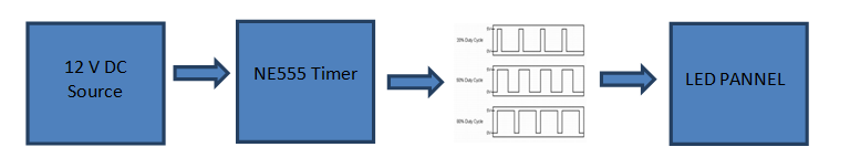
A 12V DC source is used to power the entire circuit including the 555 timer IC and the LEDs. The 555 timer is used to generate a PWM signal with the help of a few passive components.
The generated PWM Signal is then applied to a bunch of LEDs and based on the Duty Cycle of the PWM Signal, the intensity of the LEDs can be high or low.
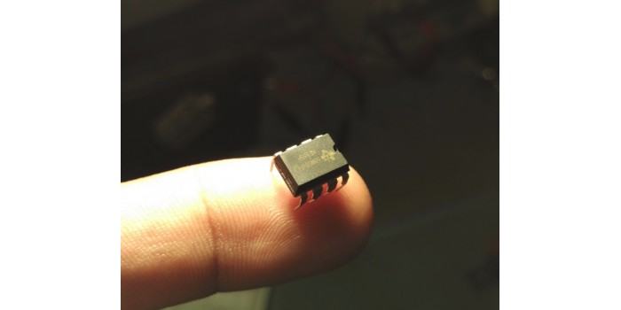
A Brief Note on 555 Timer IC
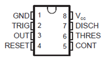
The 555 Timer is an 8-pin Integrated Circuit available in Dual-in-Line Package originally developed by Signetics. It is one of the most popular ICs and is used for a variety of applications like Timer, Oscillator and Pulse Generation.
Pin Diagram of the 555 Timer IC is shown in the following image. The pin 8, which is the VCC pin, is used to give the main supply voltage to the IC. The operating voltage may vary from 3v to 15V. Pins 2, 6 and 7 are the Trigger, Threshold and the Discharge Pins.
Pin 4 is the Reset pin and it is used to reset the complete IC. It is an active LOW Pin. The output of the IC can be taken from the out pin i.e. the pin 3. Pin 5 is the Control Pin.
The 555 Timer IC can work in three different modes of operation: Astable, Monostable and Bistable operations. It has features like timing for micro seconds through hours, adjustable duty cycles and ability work in various voltage levels etc. It has a wide range of applications like lamp dimmers, motor control, joysticks etc.
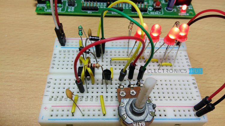
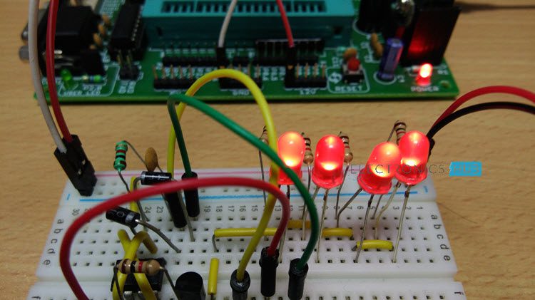
Circuit Diagram of PWM LED Dimmer Using 555
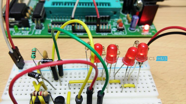
Components Required
- 555 Timer IC
- 1KΩ Resistor x 6
- Red LEDs x 4
- 2N2222 NPN Transistor
- 0.1μF Capacitor
- 0.01μF Capacitor
- 50KΩ Potentiometer
- 1N4148 Diodes
- 12V Power Supply
- Mini Breadboard
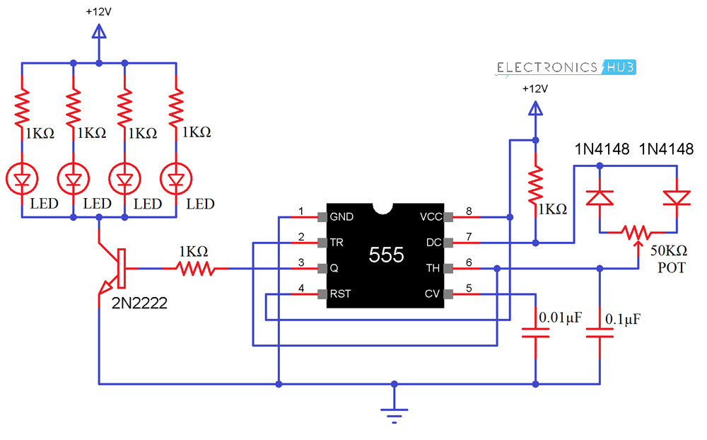
Circuit Design
- The 12V DC supply is given to the VCC Pin for operating voltage of 555 timer. The reset pin also directly connected to the 12V as shown in the circuit diagram. For resetting the IC, in case of an error while circuit is working, connect the RESET pin to GND for a Second and then connect it back to 12V.
- Pin 5 or the voltage control pin is not used in this application. Hence, a decoupling capacitor of 0.01μF is connected between pin 5 and GND.
- The Trigger pin (Pin 2) and threshold pin (pin 6) are shorted and the Wiper Terminal of the POT is connected here. Also, a 0.1μF Capacitor is connected between Pin 6 (or Pin 2) and GND.
- Now, one terminal of the POT is connected to anode of a Diode (preferably 1N4148) while the other terminal of the POT is connected to cathode of another diode.
- The other ends of both these diodes are connected to the Discharge Pin i.e. Pin 7. Also, a 1KΩ Resistor is connected between Pin 7 and VCC.
- The OUT pin is connected to the LED panel through the transistor.
Working of PWM LED Dimmer using 555
Here in this project, the 555 Timer is made to operate in the Astable Multivibrator Mode. The 1KΩ Resistor, the 50KΩ POT and the 0.1μF Capacitor connected with respect to Pins 2, 6 and 7 will play an important role.
Based on the charge and discharge timings of the Capacitor, a PWM Signal is generated at the OUT Pin i.e. Pin 3 of the 555 Timer IC. The output of the 555, which is taken form pin 3, is connected to the led panel through the NPN Transistor (2N2222 is used here) and a 1KΩ resistor.
The 1KΩ resistor is used to limit the base current of the transistor and transistor is used as an amplifier to limit or enhance the current which is given to the LED panel.
Unbiased Electronic Dice with LEDs
Playing with dice is an age old game. We all love to play with it too. Playing with dice needs us to pick up a dice and make sure that it is unbiased. Making a block as a dice and cutting it clearly to make sure that it is unbiased is all an old story. The dice becomes biased if the shape is not cut well.
Also, the dice can become biased due to deformations. If it is a wooden die, it can deform due to dampness in the atmosphere or due to mechanical stress. To solve all these problems which we have with a conventional dice, we have made a dice circuit which solves all the problems of a conventional dice.
Now, we are going to show you an electronic LED dice which is nearly unbiased. There is no chance to cheat as the circuit operates at such a high speed that the circuit is almost imperceptible to the human eye. There is also little maintenance and there is hardly any impact on aging of the circuit. The frequency may vary a bit with change in power supply voltage, aging of the active and passive components but still the randomness will be preserved without any trouble.
Electronic LED Dice Circuit Diagram:
Circuit Diagram of Unbiased Digital Dice with LEDs –
This circuit uses 555 timer as an astable multivibrator. In this mode, the circuit is arranged with R2=100 k-ohm, R3=100 k-ohm and C2=0.1 uF.
With this configuration, the circuit operates as a clock with a frequency in order of kilo hertz. This means that the circuit produces a clock cycle of about 0.000210 seconds which is imperceptible to the human eye. We cannot observe the values which change at that faster rate so there is hardly any possibility of getting the dice biased.
The clock pulses are given to a counter cum decoder circuit IC 4017 with the seventh output given to reset. It has nine possible outputs out of which, the seventh is given to reset because we only need a count upto 6 as a dice has six faces only. The first six outputs are given respectively to the LEDs so that the respective LED will glow for the corresponding count. If the count is 1, LED-1 will glow. If the count if 2, LED-2 will glow and so on until the sixth count. When the count is six, the sixth LED will glow and after that for the next clock pulse the counter will advance and the count increments to seven. In this count, the circuit resets itself as the seventh count is given to the reset pin which is PIN-15. Let me tell you that the power supply pin and ground are not shown in the circuit diagram as it is the schematic generated by the software Proteus. However, the power supply of 9V is given to the 16th pin of IC 4017 and the 8th pin of IC 4017 is given to ground.
This is how the circuit functions and you can increase the frequency of the circuit if you feel that you need more randomness so that it is very hard to perceive. This circuit can be implemented on a general purpose PCB with a 9V DC power supply.
XO____XO XXX How to Generate PWM with variable Duty Cycle and Frequency Using IC 555
555 IC is an extremely useful and versatile device which can be applied for configuring many useful circuits in the field of electronics. One of the most useful feature of this IC is its ability to generate PWM pulses in which we can vary duty cycle and frequency according to our needs.PWM stands for pulse width modulation, the process involves the control of width of pulse and frequency of generated waveform.It can be seen in SMPS power supplies for controlling the output voltage to precise levels.It is also applied in LED driver circuits for enabling LED dimming functioning. It's extensively used in buck/boost topologies for deriving step down or step up voltages without using bulky transformers.
So now the question arises how do we generate a pwm signal?
How to Use IC 555 for Generating PWM Outputs
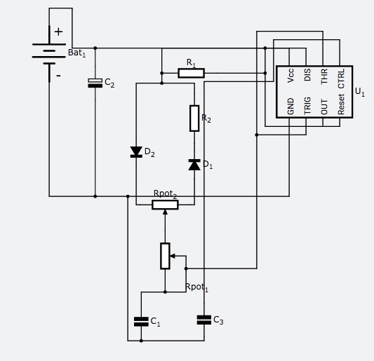
For generating PWM signal we are going to generate a square wave in which we can control width of pulse i.e. Duty cycle, and frequency. This is done through the below circuit.
Circuit diagram:
We are supplying +9Volt as input to IC555 timer but we can give input from +4.5 volt to +16 volts, it depends on output waveform we desire. Say we need an output waveform of +12Volts then we will give input as +12volts.
Components used are:
U1 - IC555 Timer
Capacitors:
C2 - Electrolytic capacitor of 10uF 100Volts
C1 - Ceramic capacitor of 10uF
C3 - Ceramic capacitor of 0.1uF
Resistors:
R1 - 4.7 K ohms
R2 - 470 ohms
Diodes:
D1 - D2 - 1N4148
Potentiometer:
P1 - P2 - 100k
P1 and P2 are variable potentiometers Rpot1 and Rpot2 respectively.
I had used 100k potentiometers but you can also use 1k or say 1M potentiometers, it all depends upon the resolution you want, more precise resolution you require, more should be the value of potentiometer.
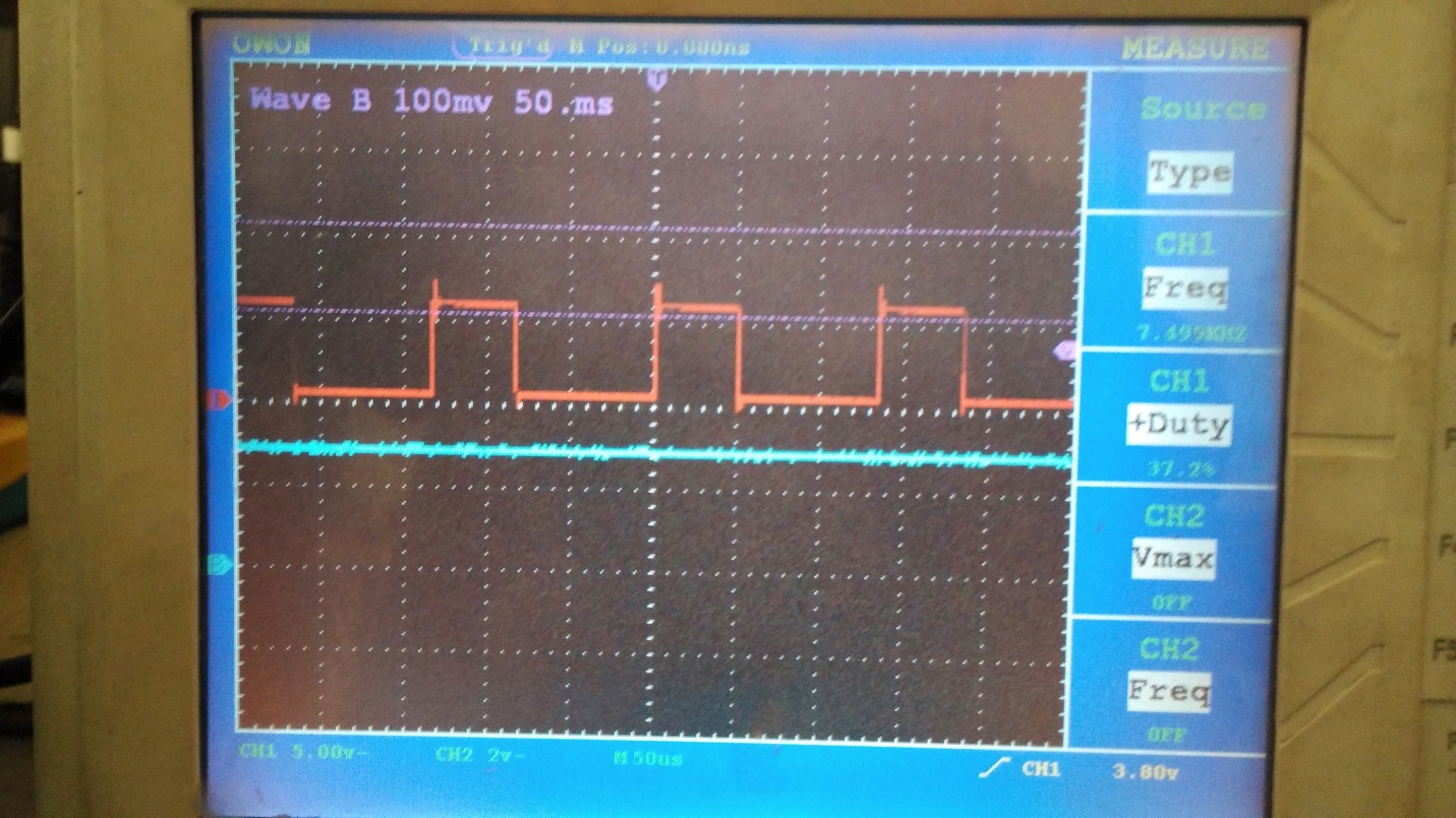
Now by varying the potentiometers Rpot1 and Rpot2 we can vary Duty cycle and frequency respectively of the output waveform as shown below. If we want more frequency we have to reduce size of C2 electrolytic capacitor, C2 capacitor and Rpot1 and Rpot2 are known as Timing circuit, by varying Rpot1, Rpot2 and C2 we can get different different frequencies from 1HZ to 1Mhz.
Frequency depends upon the formula:
Freq = 1.44 / ((R1 + R2) * C)
Output waveform:
Led Dimmer Circuit Diagram Best Of Dimmer Switches Electrical 101
Led Dimmer Circuit Diagram Best Of Dimmer Switches Electrical 101. This best image collections about Led Dimmer Circuit Diagram Best Of Dimmer Switches Electrical 101 is available to download. We collect this best image from internet and choose the best for you. Led Dimmer Circuit Diagram Best Of Dimmer Switches Electrical 101 photos and pictures collection that posted here was carefully selected and uploaded Led Dimmer Circuit Diagram Best Of Dimmer Switches Electrical 101, take your time and find the best Led Dimmer Circuit Diagram Best Of Dimmer Switches Electrical 101 images and pictures posted here that suitable with your needs and use it for your own collection and personal use. Led Dimmer Circuit Diagram Best Of Dimmer Switches Electrical 101.
Led Dimmer Circuit Diagram Luxury Soldering Iron Temperature Controller Electronics.
+++++++++++++++++++++++++++++++++++++++++++++++++++++++++++++++++++++++++++++++++++++
e- Calm with LED Dimmer and Panel Basic Television Digital ( e- MICON = e- Monotonic Vision )
+++++++++++++++++++++++++++++++++++++++++++++++++++++++++++++++++++++++++++++++++++++++++++
thank you for your valuable information
BalasHapuspower transformer manufacturers