


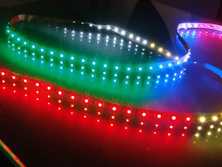
LED Display
LED Display (light-emitting diode display) is a screen display technology that uses a panel of LEDs as the light source. Currently, a large number of electronic devices, both small and large, use LED display as a screen and as an interaction medium between the user and the system. Modern electronic devices such as mobile phones, TVs, tablets, computer monitors, laptops screens, etc., use a LED display to display their output.
LED Display is one of the main screen displays that are being commercially used. The biggest advantage of the LED display is its efficient and low-energy consumption, which is especially needed for handhelds and chargeable devices such as mobile phones and tablets. An LED display consists of a number of LED panels that, in turn, consist of several LEDs. LEDs have numerous advantages over other light-emitting sources that can be used alternatively. Aside from being power efficient, LEDs produce more brilliance and greater light intensity. LED Display is different from the vacuum fluorescent display used in some consumer electronics such as car stereos, videocassette recorders, etc., and, hence, these two should not be confused with each other.
Monitor
A monitor is an electronic visual computer display that includes a screen, circuitry and the case in which that circuitry is enclosed. Older computer monitors made use of cathode ray tubes (CRT), which made them large, heavy and inefficient. Nowadays, flat-screen LCD monitors are used in devices like laptops, PDAs and desktop computers because they are lighter and more energy efficient. A monitor is also known as a screen or a visual display unit (VDU).
The advent of display technology has paved the way for the continuous evolution of the monitor, whether it's for computers, television, mobile devices or any device that has a display. The current contenders for top-tier technology being used for display devices includes Super LCD 3 (SLCD3) and Super AMOLED. It should be noted that LED displays are actually just a kind of LCD display that use LED lights as backlight illumination.
The quality of a monitor's performance is assessed using a few key factors:
- Aspect Ratio: This is the relation of the vertical length to the horizontal length of the monitor (e.g. 16:9 or 4:5).
- Dot Pitch: This is the distance between each pixel in every square inch that's displayed. The shorter the distance, the sharper and clearer the images are.
- Display Resolution: Also known as dots per inch (DPI), this determines the number of pixels per linear inch. The maximum number of pixels is determined by the dot pitch. This determines the number of pixels the display screen can accommodate.
- Size: This aspect is determined by the display screen’s diagonal measurement.
Active-Matrix OLED (AMOLED)
Active-matrix OLED (AMOLED) is a display technology used in mobile devices, digital cameras, media players, and televisions. It employs active matrix in addressing pixels and uses a specific type of thin film technology in which organic compounds form electroluminescent material. AMOLED stands for active matrix organic light emitting diode.
The AMOLED display is made up of pixels integrated with, or deposited into, a thin film transistor (TFT) array. OLED technology is basically an LED using organic compounds as an emissive electroluminescent layer. The organic compound uses generated light in response to the passage of an electric current.
The AMOLED display is made up of pixels integrated with, or deposited into, a thin film transistor (TFT) array. OLED technology is basically an LED using organic compounds as an emissive electroluminescent layer. The organic compound uses generated light in response to the passage of an electric current.
The TFTs act as switching devices to actively maintain the pixel state while addressing other pixels. The two common TFT backplane technologies used are the non-crystalline thin-film silicon and the polycrystalline silicon. These technologies aid in the fabricating of active matrix backplanes for flexible plastic substrates. Flexible plastic substrates are crucial in producing flexible AMOLED displays.
The AMOLED technology provides a higher refresh rate than its passive-matrix counterpart and consumes less power. This advantage gives it an edge to be the technology of choice in the manufacture of mobile devices. Other advantages are:
The AMOLED technology provides a higher refresh rate than its passive-matrix counterpart and consumes less power. This advantage gives it an edge to be the technology of choice in the manufacture of mobile devices. Other advantages are:
- Higher perceived luminance.
- Higher contrast ratio, although reading in direct sunlight may pose a problem.
- Wider viewing angle compared to conventional displays.
One major disadvantage with the AMOLED is the limited lifetime of the organic compound used. The blue OLEDs reduce to half their brightness after 14,000 hours. This is compared to conventional LCDs, which usually dim to half after 25,000 to 40,000 hours.
Diode Matrix
A diode matrix is a specific physical setup, a grid of wires used for implementing read-only memory. In this two-dimensional wire grid, each connection or intersection of wires either has a connecting diode, or an isolated design.
Diode matrices have been used as control stores in various types of computers and electronic devices. A diode matrix was a common type of memory store architecture in early computers. It has also been used in items like programmable calculators. A diode matrix can be part of a programmable logic array chip. Some of these types of wire designs are still used in modern microprocessors.
Organic Light-Emitting Diode (OLED)
An organic light-emitting diode (OLED) is a solid-state light device that makes use of flat light emitting technology with the help of two conductors between which a series of organic thin films are kept. Unlike other display modes, an OLED does not require backlighting. Because of its low power consumption and great brightness, OLED is used as a backlight source in LCD displays, electronic equipment, signaling as well as in general lighting.
When current is transmitted to the electrodes, the movement of charges happens with the influence of the electric field. Electrons depart from the cathode, whereas holes depart from the anode in the opposite direction. Photons are created by the recombination of these charges whose frequency is decided by the highest occupied molecular orbital (HOMO) and the lowest unoccupied molecular orbital (LUMO) energy levels of the molecules being emitted. This results in the transformation of power to light.
Advantages of OLED over LCD:
Advantages of OLED over LCD:
- OLED-based screens can be significantly thinner, resulting in lighter weight.
- OLED has better contrast and allows a higher refresh rate.
- OLED allows new display capabilities like ultra-thin, transparent displays.
- Power consumption is very low.
- OLED-based screens provide a fuller viewing angle and are also much brighter.
- Durability is better. OLEDs can work in broader temperatures as well.
Display Monitor
A display monitor is an electronic device used to display video output from computers. Display monitors are used in many computer devices, ranging from personal computers (PC) and laptops to small handheld mobile devices, like cellphones and MP3 players.
A display monitor is also known as a computer screen or display screen.
A display monitor is comprised of the following:
- Display module: Often the type that uses thin film transistor liquid crystal display (TFT-LCD) technology
- Circuitry
- Case or enclosure
Originally, display monitors were found only on computer devices. As screen technology has become smaller, cheaper and more powerful, display monitors have increasingly been added to a variety of devices.
Until the early 2000s, the prevailing technology was cathode-ray tube (CRT), which was less bulky with a smaller resolution and used more power. Liquid crystal display (LCD) is thinner and consumes less power but was more expensive. So, throughout the 1990s, LCDs were only used in laptops, where portability justified its pricing. Other technologies used are plasma and organic light-emitting diode (OLED).
Many companies brand their monitors as "LED," which means that LED is used for screen backlighting, versus traditional fluorescent lighting.
Monitor performance is measured according to the following main factors:
- Luminance: Brightness in candelas per square meter (cd/m2 or Nits)
- Aspect ratio: Ratio of vertical and horizontal length as in 4:3, 16:9, 16:10
- Display resolution: Number of pixels per square inch
- Refresh rate: Number of times the display changes
- Response time: The time it takes for a pixel to be active (on) to inactive (off) and vice versa. Measured in milliseconds.
- Contrast ratio: Ratio of luminosity of the brightest (white) to darkest color (black) that can be produced by the monitor
- Power consumption: Measured in Watts
Viewing Angle
The viewing angle of a device or piece of hardware is the maximum angle where users can still view the display well. Different types of devices and displays have different viewing angles, due to things like pixel brilliance, the flow of current through display materials and the general engineering of the ways that the screens present themselves as interfaces.
Along with the maximum viewing angle, many factors also sometimes specify a “viewing cone” as a set of angles at which the display works well. In some cases, the viewing angle is relatively slight – for instance, with many personal laptop computers, even a relatively insignificant angling of the screen decreases the quality of the display picture. Some critics of LCD technology also point to the limited viewing angle of many screen models. One other place that viewing angle is important is in the evolution of curved display screens, as with OLED panorama televisions. By actually making the screen curved, designers are trying to enhance the process, which requires dealing with viewing angles to let users get a good experience from a wider “cone” of positions.
USING LED ON TV ( e- MICON )
Traditional Video Walls
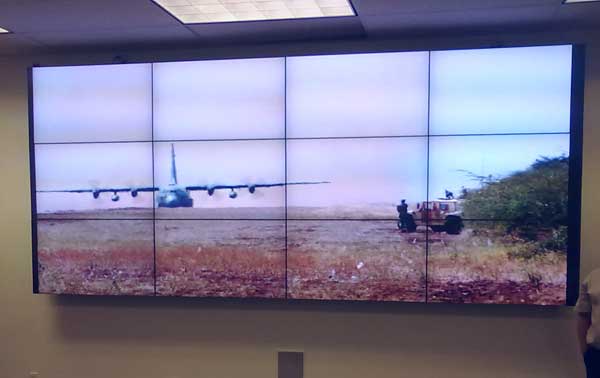
First, let’s look at why traditional video panels, made up of several LCD panels with thin bezels and frames, have become popular. The main reason is simple: they have been the lowest cost, reasonable-quality way to do video and information displays in large sizes. You can see them as backgrounds in almost every newscast, in shopping mall displays, as command and control center dashboards, lecture halls, and even in some hotel lobbies.The newer video walls use LED panels as the light source behind the LCD glass – so they are reasonably reliable and their bezel thickness or window frame is rather thin(and they keep getting smaller). So why the need for a better solution? Let’s look at their disadvantages.
Traditional LCD video walls have bezel lines and challenges with calibration
Downsides of Traditional Video Walls:
1. Smaller video walls like a 2 x 2 panel configuration can now be done with a single, cost effective LCD panel
2. Each panel in the video wall must be calibrated and re-calibrated on a regular basis to maintain even brightness and color uniformity (see picture above)
3. No matter how small the bezel width between the panels, it is still a break in the image and a visual distraction to the message
4. As soon as you go larger than a 3 x 3 panel configuration, the fine pitch of the panel is not able to be utilized nor is it generally even needed – because most video walls are designed to be viewed from a distance
5. Most video walls are very directional – color, contrast and brightness falls off unless you are directly in the front and center of the display
New Cost-Effective Alternatives to video Walls

Larger, brighter, and more vivid displays are now possible at almost the
same cost as traditional thin bezel video walls and without the annoying lines in the image. (Note: the display image above is purposely overexposed so you can see the environment – which was very bright but looks dark in comparison to the very bright image.)
same cost as traditional thin bezel video walls and without the annoying lines in the image. (Note: the display image above is purposely overexposed so you can see the environment – which was very bright but looks dark in comparison to the very bright image.)
Fine-Pitch Direct-View LED Video Displays
Direct-view LEDs have been around for quite a few years. However, it has only been recently that fine-pitch indoor-viewing LED panels have become more affordable. Outdoor direct-view LED screens are familiar to everyone – most have seen them as electronic billboards, very large stadium replay screens, and those really large video screens in Times Square and the Las Vegas strip. However, that is not what we are talking about here – but they are related. The outdoor direct-view LED screens are bright, colorful, and have great contrast, but if you get close to one, they are very pixelated and annoying. That’s because the outdoor direct-view LEDs are designed to be seen only from a distance, like 75′, 100′ or 200′ or more. But instead of talking about those, we’re talking about fine-pitch (a pitch of 3mm or smaller) direct-view LED displays . Here’s a great example to help you understand:
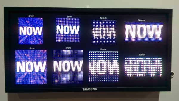
This display by Samsung, seen at DSE 2017, shows the beginning of fine-pitch direct-view LEDs in the upper left at 3mm. Typical outdoor LED billboards are 16mm or 20mm.
LEDs are Not Always LEDs!
Before we go into this next part we need to clear up a little confusion. The ads you may see for 4K flat screen TVs often just say 55″ or 75″ LED 4K TV. Those are not direct-view LED screens – those are LCD screens using white or blue LEDs as a light source for the LCD screen. That is also what is used to make most video walls – but those are special versions with very thin bezels. One of the challenges with LED/LCD TVs is that it is very difficult to get really high contrast (their blacks appear milky) and high light output (nits). The LED screens we are talking about here are red, green, and blue self-emitting Light Emitting Diodes or direct-view LEDs. We now have direct-view LED screens (indoor, fine-pitch) that have dot pitches under 1 mm. When the individual LEDs are off, they can have almost perfect blacks – unlike LCD which always has some back light scatter which displays as imperfect blacks. That means that LED screens can now have very high resolution, very high contrast, and very close viewing distances.
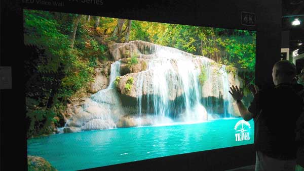
Very fine pitch direct-view LEDs, like this one at DSE 2017, are very bright and look great even as close as a few feet away. (In this image, the camera was exposed so you could see some of the LED image but the room environment is bright as well. Cameras just cannot capture both areas at the same time.)
Advantages of Fine-Pitch Direct-View LED Displays:
1. Excellent contrast that far exceeds the best LCD technology
2. Extreme brightness that exceeds even the brightest LCD displays
3. No visible bands or bezel edges in the image – just full clear images
4. Long life – typically 70,000 hours to half brightness
5. Available in 3 mm to less than 1mm – for almost any indoor viewing application
6. New LED panel screen sizes, of up to 54″, simplify large video display projects
7. New production and volume manufacturer of LEDs has made this technology competitive with some video wall projects starting this year
Conclusion
We are finding that many in the industry (traditional AV dealers) are not aware of this new trend of migrating to new fine-pitch direct-view LED displays – or are not even aware of the new price levels that are now available from some core LED manufacturers. It seems that almost every major manufacturer of flat screen panels is very aware of this migration – hence the presence of these displays in almost all of their booths at the Digital Signage Expo (DSE) this year. Unfortunately, those same manufacturers are the ones that could be left with a lot of LCD inventory if they do not keep up.
XO___XO LED MATRIX
Structure of Led Matrix
In a matrix format LEDs are arranged in rows and columns. You can also think of them as y and x coordinates. Lets assume we have 4x4 matrix. Rows would be marked from A to D and columns from 1 to 4. Now we can address each LED by row and column. Top left led would be (A,1). Bottom down led would be (D,4).
Led matrices come in two flavors. Common-row anode (left) and common-row cathode (right).
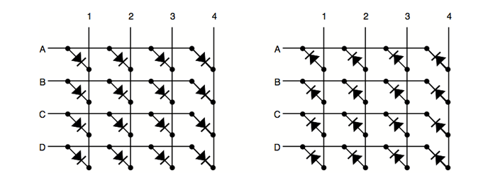
Figure above shows the different configurations. The difference between these two configurations is how you lit a led. With common-row anode current sources (positive voltage) are attached to rows A..D and currents sinks (negative voltage, ground) to columns 1..4. With common-row cathode current sinks are attached to rows A..D and currents sources to columns 1..4.
For example. To light bottom down led (D,4) of common cathode matrix you would feed positive voltage to column 4 and connect row D to ground. For sake of clarity I will using common-row cathode in examples for the rest of this article.
Building a LED Matrix
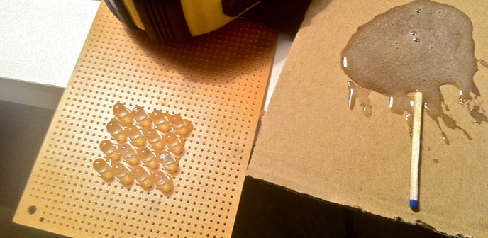
To build a 4x4 common-row cathode matrix you will need 16 LEDs, four resistors, some headers and prototyping board. I started by gluing the leds to prototyping board with epoxy glue. This way it is easier to have LEDs beautifully aligned. When gluing the leds make sure long and short legs are aligned the same way.
When glue is dry it is time to bend and solder. First bend all cathodes to left as close to prototyping board as possible. Solder all cathodes in each row together. When cathodes are ready, bend all anodes. Anodes must not touch cathodes. I used piece of plastic tubing to help bending the anodes to form a bridge above cathodes.
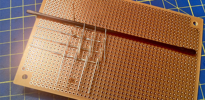
Now solder together all anodes in each row. Solder the headers and connect cathode rows directly to the header.
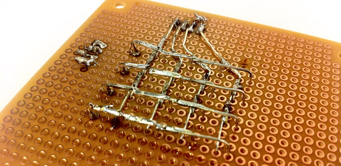
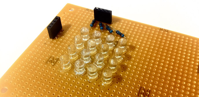
Anode rows are connected to header with current limiting resistors. Value of the resistor depends on the LED used. Check the LED datasheet for forward voltage and current. LED calculator will help you finding out correct resistor. Matrix is now ready for testing.
Addressing Single LED
Connecting ground to row A and positive voltage to column 1 will light the top right LED (A,1).
Connecting ground to row D and positive voltage to column 4 will light the bottom down LED (D,4).
Intuition would say lighting the both (A,1) and (D,4) at the same time is just connecting all the four wires. This is not the case. There are four LEDs which are lit. This is because current is also flowing through (A,4) and (D,1).
Multiplexing and Persistence of Vision
Multiplexing can be used to display arbitrary patterns with led matrices. Multiplexing is sometimes also called scanning. It scans rows (usually from up to down) and lights needed leds only in one row at time. Something like following:
- Start by having everything disconnected.
- Connect positive voltage all the needed columns.
- Connect row to ground. This lights the needed leds in the row.
- Disconnect the row and all columns.
- Do the same steps one by one to all rows and then start from the beginning.
Do this slowly and you would see blinking LED rows. Do it really fast and human eye can see the whole pattern. Phenomenon is called persistence of vision.
What is an LED Display?
What is a LED?
A: LED is an acronym for Light Emitting Diode. A LED is an electronic source of light and is not a light bulb. The first practical visible-spectrum LED was created by Nick Holonynak, Jr. in 1962 and has been refined over the years, resulting in the diode utilized today. LEDs present many advantages over other light sources, including lower energy consumption, longer lifetime, improved brightness, smaller size, faster switching and greater durability and reliability.
What is a Pixel?
A: A pixel or picture element is the smallest unit of picture that can be represented or controlled. In terms of a LED display the smallest unit of picture (pixel) is a single (Red or Amber) LED for the monochrome unit and a group of LEDs (Red, Green & Blue) for the color units. These pixels are arranged in a two dimensional (rows x columns) grid call a Pixel Matrix. A display with more pixels generally has more LEDs, resulting in higher resolution content.
What does the term “pitch” refer too?
A: The pitch is the center-to-center distance between pixels. Traditionally given in millimeters some have provided in inches. Focus Digital Displays provides pitches ranging from 16mm to 35mm thus providing an appropriate solution for any application. The smaller the pitch the tighter the pixel spacing resulting in a higher resolution display.
What does the “viewing angle” of a LED display mean?
A: The viewing angle is the maximum angle at which an LED display can be viewed with acceptable visual performance. That being said, a LED display is brightest when being viewed head on, and though it loses its intensity as you move away from the center axis, the information can still be read up to a defined point. This point, the viewing angle, is two (2) times the ½ brightness angle. Focus Digital Displays offers LED displays with extra wide viewing angles; 140o horizontal and 70o vertical.
What is a monochrome LED display?
A: A monochrome LED display is a single color display that provides various shades of a single color. Traditionally, monochrome LED displays area available in Red or Amber and utilized mainly to communicate sharp bold text. Focus Digital Displays monochrome products provide 4,096 shades of either Red or Amber for improved graphic capability.
What is a color LED display?
A: A color LED display is a display comprised of three colors, Red, Green & Blue, working together to create the full color spectrum. Each of these colors is represented by a LED in every pixel, therefore tripling the total number of LEDs to a comparable monochrome display. Focus Digital Displays’ color LED displays provide the deepest color palates in the industry, resulting in the most lifelike color content available.
Which LED display is best for me?
A: To determine which LED display is best for a given application, there are a number of items to consider, such as audience, location, size and the desired messages to communicate. Once these have been addressed, then we can select which Focus Digital Display will provide the maximum return on your investment.
What is the best way to communicate my information on a LED display?
A: Bold and simple content is the sure fire way to ensure your message is received. Whether you are utilizing a FocusMono for eye-catching text or a FocusColor product for dynamic animation or video, you cannot go wrong with the “little is more” approach. If you would like to leave it up to the experts, then contact our graphics department about one of our Custom Content Creation Packages.
How do I know if my city will allow me to put up a LED display?
A: We will handle it! Focus Digital Displays employs Digital Display experts who have experience in reviewing and working with municipal sign ordinances to determine project feasibility. Ultimately it is your responsibility to adhere to the local laws; however, we will uncover any and all information pertaining to your project to ensure you stay in compliance with your local government.
How much does a LED display cost?
A: Due to the numerous options available it is difficult to answer the question without addressing the items in “Q: Which LED display is best for me?” above. A better way to view this question is: where will the funds come from to purchase the LED display? Many customers look at the purchase of a new LED display as strictly a capital expenditure but when you consider the advertising and communication benefits then considering your marketing/advertising budget as well only makes sense. It is also important to note that Focus Digital Displays provides various financing options too.
PIXELS LED
When it comes to direct-view LED displays, pixel pitch is a technical unit of measurement, but the term has also become a primary way for manufacturers to distinguish and market their products. Pixel pitch helps distinguish tiers of LED displays for buyers and signifies an increase in resolution and image quality.
Armed with all of the information on pixel pitch, decision-makers can easily weight their options regarding display size, viewing distance, resolution and cost.
Pixel Pitch Basics
Pixel pitch is the distance in millimeters (mm) from the center of an LED cluster, or package, to the center of the next LED package above, below and beside it. The LED packages are mounted on circuit boards and backplates, known as modules.
LED videowalls are put together by grouping these modules into larger display surfaces, fixing them together like seamless tiles. The more LED packages that are mounted together on one module, the more it will cost. Much of the manufacturing costs for LED displays relate to the cost of the tiny LED lights inside the modules, the wiring as well as the manufacturing processes.
Pitch and Display Resolution
When it comes to display assembly, the overall footprint of a videowall ties directly to the pixel pitch of the LED displays. This is especially true if you are looking to create a videowall with a specific resolution, such as a 4K presentation screen in a boardroom.
How to Plan and Deploy LED Digital Signage

An LED display module with a 1.5mm pitch has more pixels per module than, for example, a 4mm product, and will, therefore, realize 4K resolution of 3,840 x 2,160 pixels in much less physical space. This not only helps organizations achieve a higher resolution but also requires fewer materials for assembly and reduces the videowall’s size requirements.
Pitch and Viewing Distance
LED pitch also matters when it comes to average viewing distances. When a person gets relatively close to an LED display, it may be possible to see the individual pixels and the black gaps between them. When that happens, the viewing experience is degraded. Ideally, the average viewer is far enough away that the gaps aren’t visible, and the visuals still look crisp and seamless.
There are multiple theories about the exacting measurement and ratio, but a good rule of thumb when thinking about pitch and viewing distance is that 1mm in pitch equals 8 ft of viewing distance.
Viewing distance matters not only for viewing quality but for project planning and cost. For example, a 1.5mm fine-pitch LED display looks amazing, but if day-to-day viewers, on average, will be at least 30 feet away, then there is no reason to invest in a premium-priced installation. Instead, a less-expensive 3mm display will look just as great as the 1.5mm option at that distance.
How Fine Will It Get?
LED manufacturers generally say the buyer sweet spot, at least right now, for fine-pitch LED displays, is roughly 2mm to 2.5mm. This balances viewing needs and budget practicalities. For installations that will be viewed up close or where higher resolution is required, stepping up to 1.5mm pixel pitch makes sense.
Still, manufacturers are working to further refine LED technology. Samsung recently announced at CES 2018 a premium consumer TV branded as The Wall, leveraging Micro-LED technology with a pixel pitch of 0.84mm. As with many display technologies introduced in the past, Micro-LED looks set to the commercial display marketplace too after The Wall Professional appeared at ISE in February.
It remains to be seen where the limit will be reached with fine pixel pitch LED displays, but the significant advances made in recent years mean direct-view LED is now a compelling option for most environments. And it’s clear pixel pitch will continue to be at the center of the LED technology conversation.
Display Decoder
A Digital Decoder IC, is a device which converts one digital format into another and one of the most commonly used devices for doing this is called the Binary Coded Decimal (BCD) to 7-Segment Display Decoder.
7-segment LED (Light Emitting Diode) or LCD (Liquid Crystal Display) type displays, provide a very convenient way of displaying information or digital data in the form of numbers, letters or even alpha-numerical characters.
Typically 7-segment displays consist of seven individual coloured LED’s (called the segments), within one single display package. In order to produce the required numbers or HEX characters from 0 to 9 and A to F respectively, on the display the correct combination of LED segments need to be illuminated and BCD to 7-segment Display Decoders such as the 74LS47 do just that.
A standard 7-segment LED display generally has 8 input connections, one for each LED segment and one that acts as a common terminal or connection for all the internal display segments. Some single displays have also have an additional input pin to display a decimal point in their lower right or left hand corner.
In electronics there are two important types of 7-segment LED digital display.
- 1. The Common Cathode Display (CCD) – In the common cathode display, all the cathode connections of the LED’s are joined together to logic “0” or ground. The individual segments are illuminated by application of a “HIGH”, logic “1” signal to the individual Anode terminals.
- 2. The Common Anode Display (CAD) – In the common anode display, all the anode connections of the LED’s are joined together to logic “1” and the individual segments are illuminated by connecting the individual Cathode terminals to a “LOW”, logic “0” signal.
Common Cathode and Common Anode Format

Electrical connection of the individual diodes for a common cathode display and a common anode display and by illuminating each light emitting diode individually, they can be made to display a variety of numbers or characters.
7-Segment Display Format

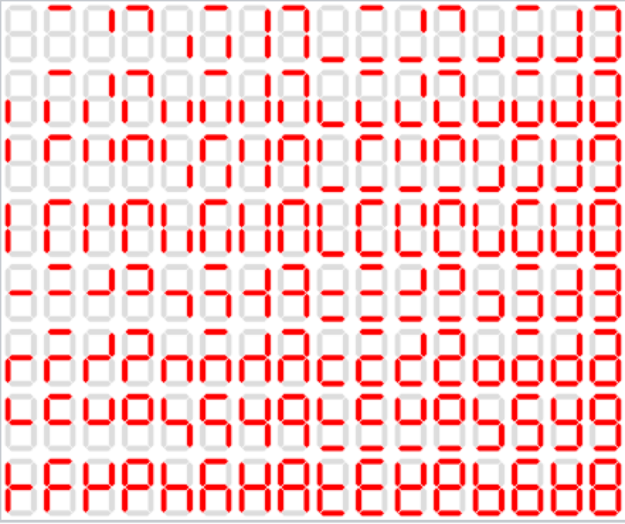
So in order to display the number 3 for example, segments a, b, c, d and g would need to be illuminated. If we wanted to display a different number or letter then a different set of segments would need to be illuminated. Then for a 7-segment display, we can produce a truth table giving the segments that need to be illuminated in order to produce the required character as shown below.
Truth Table for a 7-segment display
|
| ||||||||||||||||||||||||||||||||||||||||||||||||||||||||||||||||||||||||||||||||||||||||||||||||||||||||||||||||||||||||||||||||||||||||||||||||||||||||||||||

7-Segment Display Elements for all Numbers.
It can be seen that to display any single digit number from 0 to 9 in binary or letters from A to F in hexadecimal, we would require 7 separate segment connections plus one additional connection for the LED’s “common” connection. Also as the segments are basically a standard light emitting diode, the driving circuit would need to produce up to 20mA of current to illuminate each individual segment and to display the number 8, all 7 segments would need to be lit resulting a total current of nearly 140mA, (8 x 20mA).
Obviously, the use of so many connections and power consumption is impractical for some electronic or microprocessor based circuits and so in order to reduce the number of signal lines required to drive just one single display, display decoders such as the BCD to 7-Segment Display Decoder and Driver IC’s are used instead.
Binary Coded Decimal
Binary Coded Decimal (BCD or “8421” BCD) numbers are made up using just 4 data bits (a nibble or half a byte) similar to the Hexadecimal numbers we saw in the binary tutorial, but unlike hexadecimal numbers that range in full from 0 through to F, BCD numbers only range from 0 to 9, with the binary number patterns of 1010 through to 1111 (A to F) being invalid inputs for this type of display and so are not used as shown below.
|
| ||||||||||||||||||||||||||||||||||||||||||||||||||||||||||||||||||||||||||||||||||||||||||||||||||||||||||||||||||||
BCD to 7-Segment Display Decoders
A binary coded decimal (BCD) to 7-segment display decoder such as the TTL 74LS47 or 74LS48, have 4 BCD inputs and 7 output lines, one for each LED segment. This allows a smaller 4-bit binary number (half a byte) to be used to display all the denary numbers from 0 to 9 and by adding two displays together, a full range of numbers from 00 to 99 can be displayed with just a single byte of 8 data bits.
BCD to 7-Segment Decoder

The use of packed BCD allows two BCD digits to be stored within a single byte (8-bits) of data, allowing a single data byte to hold a BCD number in the range of 00 to 99.
An example of the 4-bit BCD input ( 0100 ) representing the number 4 is given below.
Display Decoder Example No1

In practice current limiting resistors of about 150Ω to 220Ω would be connected in series between the decoder/driver chip and each LED display segment to limit the maximum current flow. There are different display decoders and drivers available for the different types of available displays, either LED or LCD. For example, the 74LS48 for common-cathode LED types, the 74LS47 for common-anode LED types, or the CMOS CD4543 for liquid crystal display (LCD) types.
Liquid crystal displays (LCD´s) have one major advantage over similar LED types in that they consume much less power and nowadays, both LCD and LED displays are combined together to form larger Dot-Matrix Alphanumeric type displays which can show letters and characters as well as numbers in standard Red or Tri-colour outputs.
XO___XO XXX
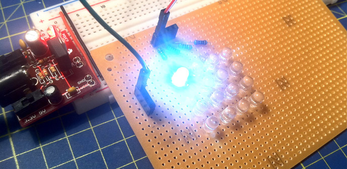
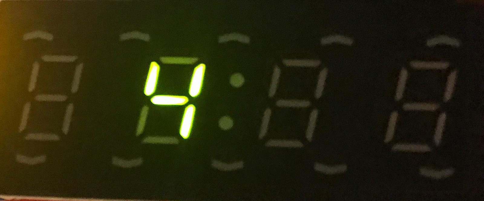
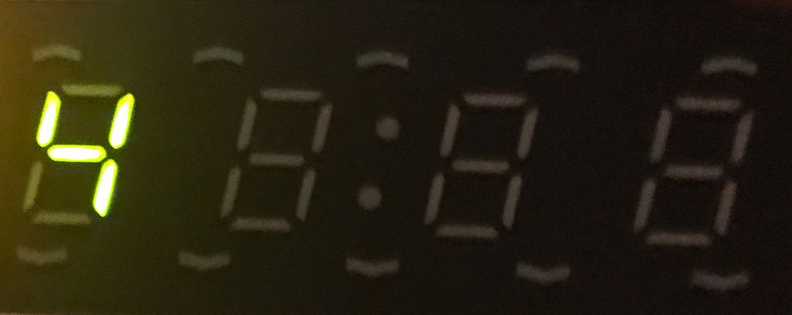
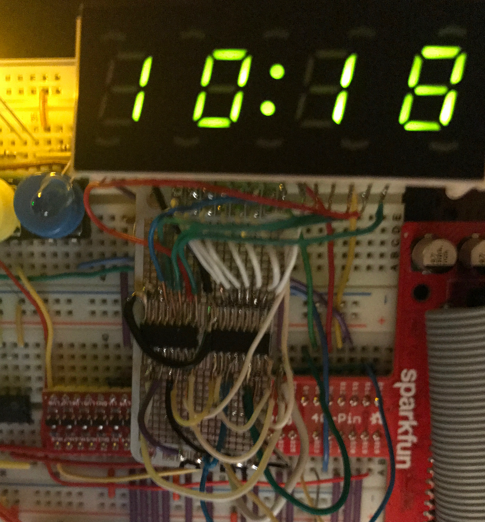
4x7-segment LED display as a digital clock using two 74HCT595 8-bit shift registers
This is a follow up to Building a 4-bit shift register from 7400 NAND gates for GPIO output port expansion on a Raspberry Pi, building a larger (16-bit) shift register to drive all of the LED segments of the display salvaged in Emerson MW8675W microwave oven teardown: salvaging the LED display,ultimately to create a digital clock driven by a Raspberry Pi.
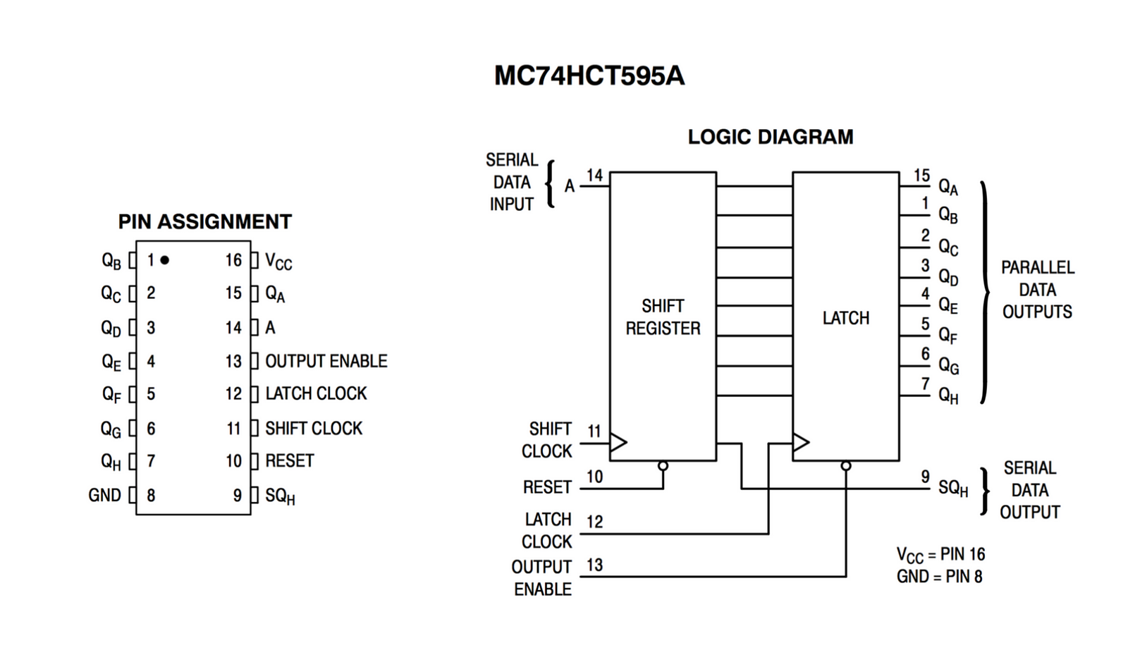
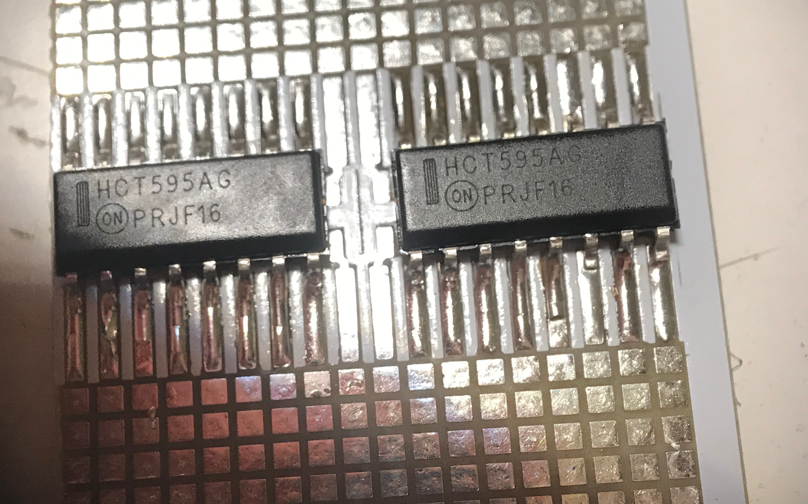
I’ll use another, more practical member of the 7400 series: the ‘595, an 8-bit shift register. Two, chained together for 16-bit total. Specifically, the “HCT” variant of the 74595, high-speed CMOS with TTL compatible logic levels. Here’s the pinout and block diagram for the datasheet of the MC74HCT595A: 8-Bit Serial-Input/Serial or Parallel-Output Shift Register with Latched 3-State Outputs and LSTTL Compatible Inputs:
Through-hole/DIP packages may be more common for casual electronics hobbyist use, but I’m striving to do more with surface-mount electronics, so I opted for the SOIC-16 package of the 74HCT595, which I soldered onto the surface-mount prototyping board ; Soldered on two, to half of a board:
Wired up power (+5 V), ground, serial input (pin #14, “A”), and both clocks (pin #12 latch clock, pin #11 shift clock) to the Raspberry Pi, in parallel with the 4-bit shift register:
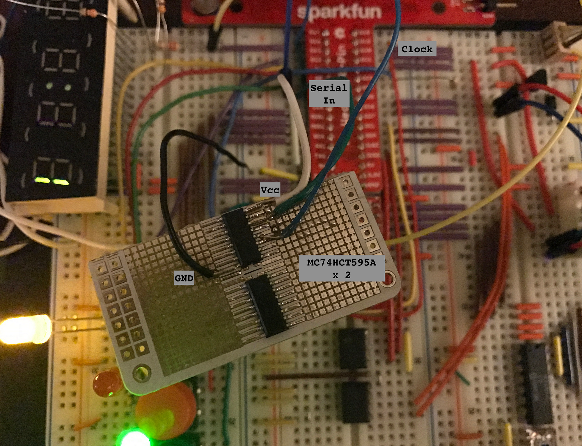
Measured Q_A (pin #15), the first parallel output, with a multimeter and confirmed the output was shifted in, as expected. Shifting is working, time to make it do something useful.
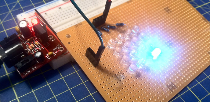
Driving the Anodes, with one 74HCT595
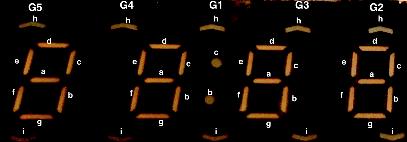
Recall the LED display pinout I reverse-engineered in Emerson MW8675W microwave oven teardown: salvaging the LED display:
- 1: G1, 2: G2, 3: G3, 4: G4, 5: G5
- 6: i, 7: h, 8: g, 9: f, 10: e, 11: d, 12: c, 13: b, 14: a
I soldered on 0603 surface-mount chip resistors, 330 Ω for to limit current to the LEDs, onto each of the parallel outputs and wired to the LED display’s anodes (positive, in whichever is most convenient to wire — the ordering will later be assigned in software), and group #5 to +3.3 V. The segments will be driven active-low, emitting a logic zero to turn them on. The active-low output enable (pin #13) is grounded so it always outputs, and the active-low reset (pin #10) is tied to power so it never resets.
For this initial test, only group #5, the leftmost digit, will be illuminated. Wrote a script to shift in 8 bits (e f g b c d i a; omitted ‘h’ for now), here group 5’s segments a, b, c, and e are lit up, after shifting in [1,0,0,1, 1,0,0,1]:
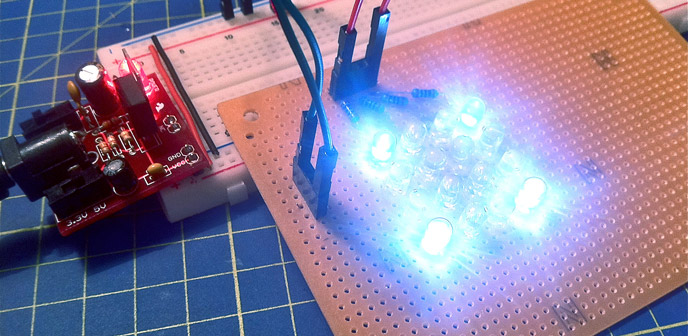
Adding another 74HCT595 for cathode control
To use all four of the digits, more parallel outputs are needed. Time to wire up the second chip, also an 8-bit 74HCT595 shift register. The serial output, SQ_H (pin #9) of the first chip connects to the serial output A (pin #14) of the second chip, altogether creating a 16-bit shift register. Plenty of bits.
First I wired Q_A of the 2nd shift register through a 330 Ω resistor to the ‘h’ segment anode, now all segments in group #5 can be driven, by 9 bits:
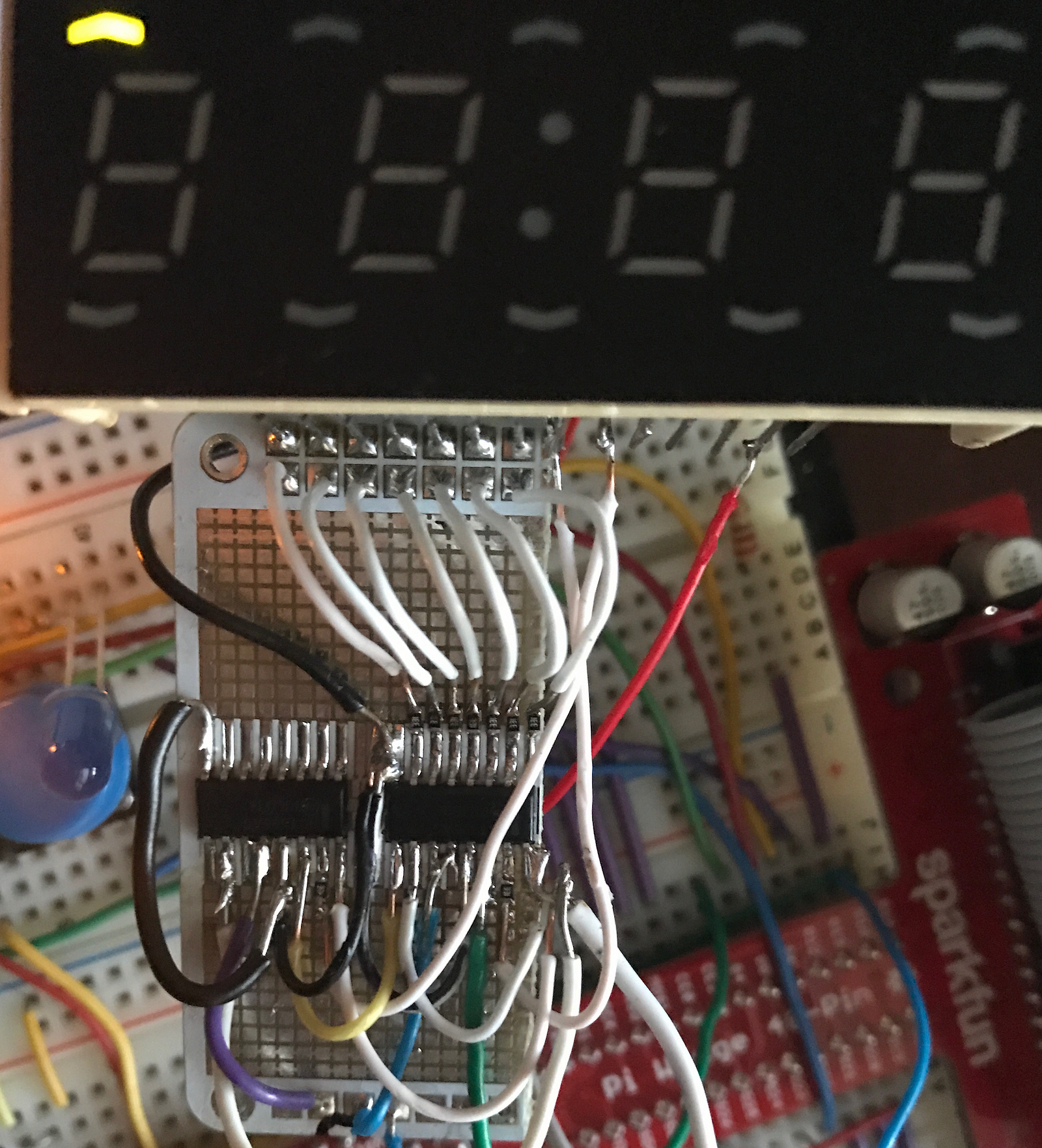
The remaining shift register outputs will be used to control the cathode(positive side) of the LEDs, corresponding to the five groups. No current-limiting resistors are needed on these outputs since the 330 Ω’s are already on the anodes.
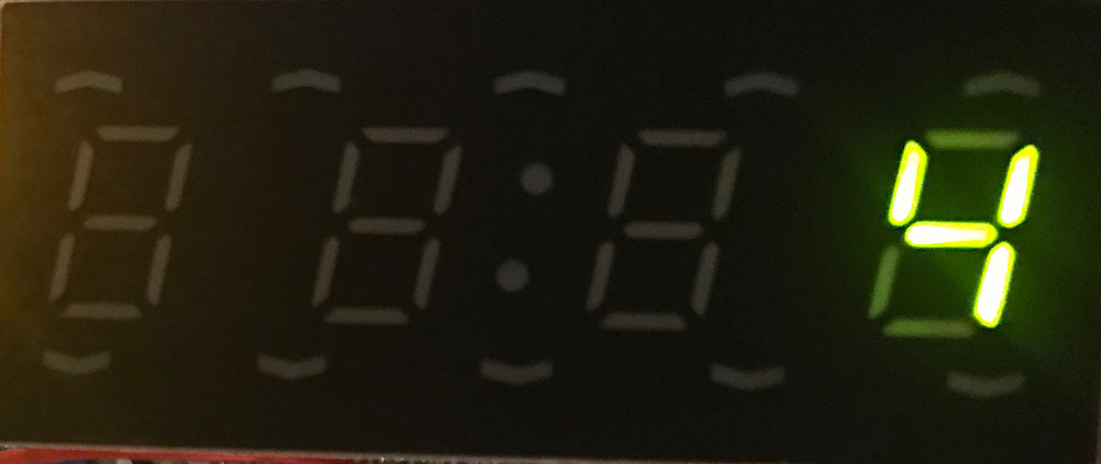
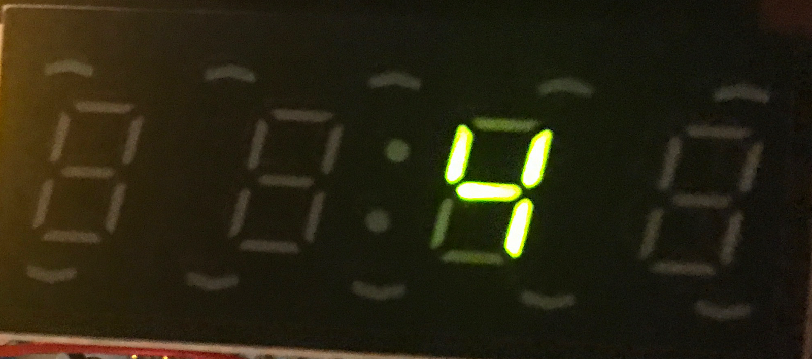
After soldering on the register outputs to the cathodes, groups can now be selected by outputting high in the leading bits, for example this is [1,0,0,0,0, 0,0,0,0, 0,0,0,0,0,0], turning on all segments of group #2:
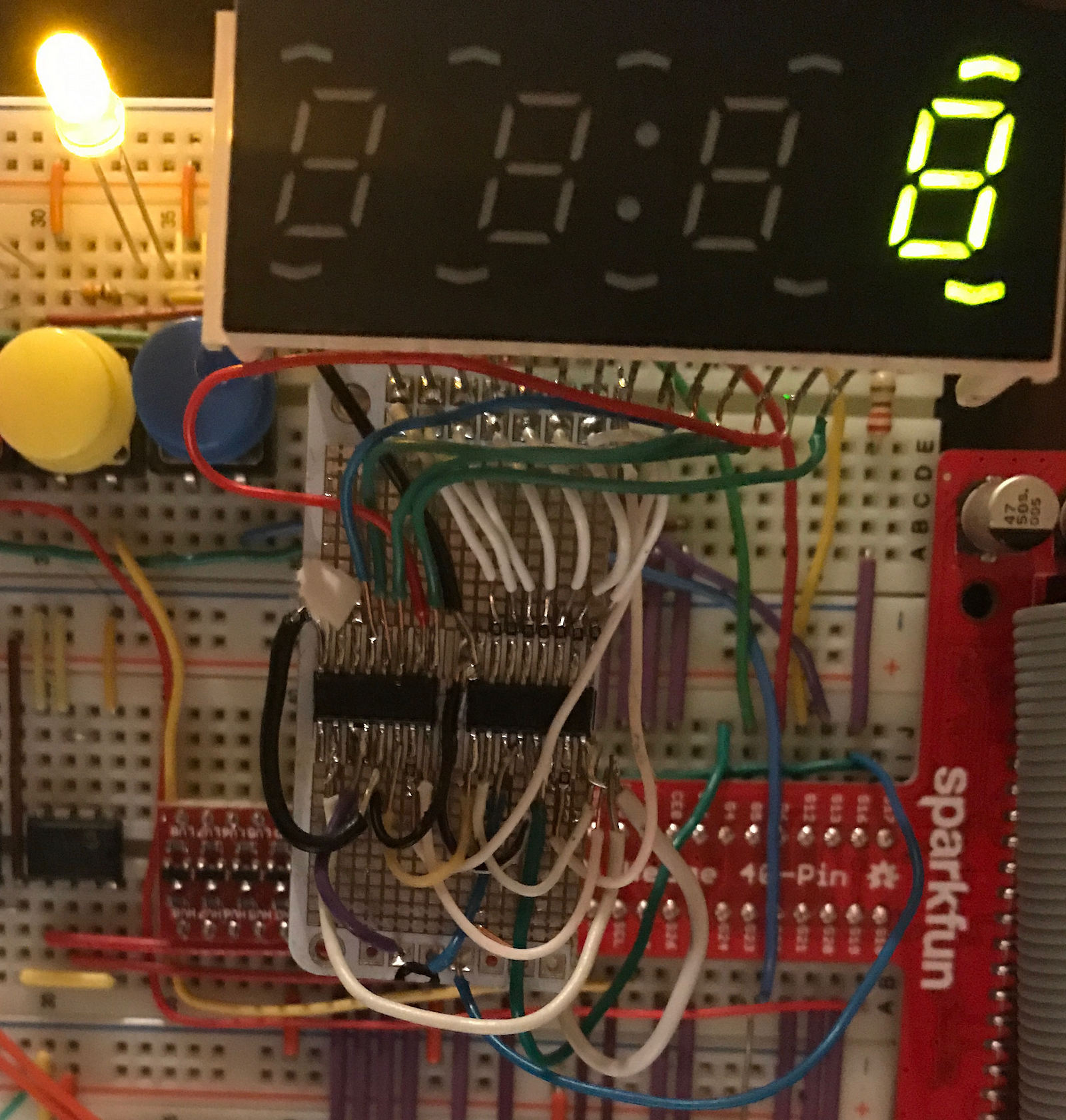
The group outputs are active-high, segment outputs are active-low, so current goes between the two logic outputs: one sources, one sinks. The 16 bits correspond to: x 2 3 4 5 1 h a e f g b c d i x, some tests/examples:
Extra outputs
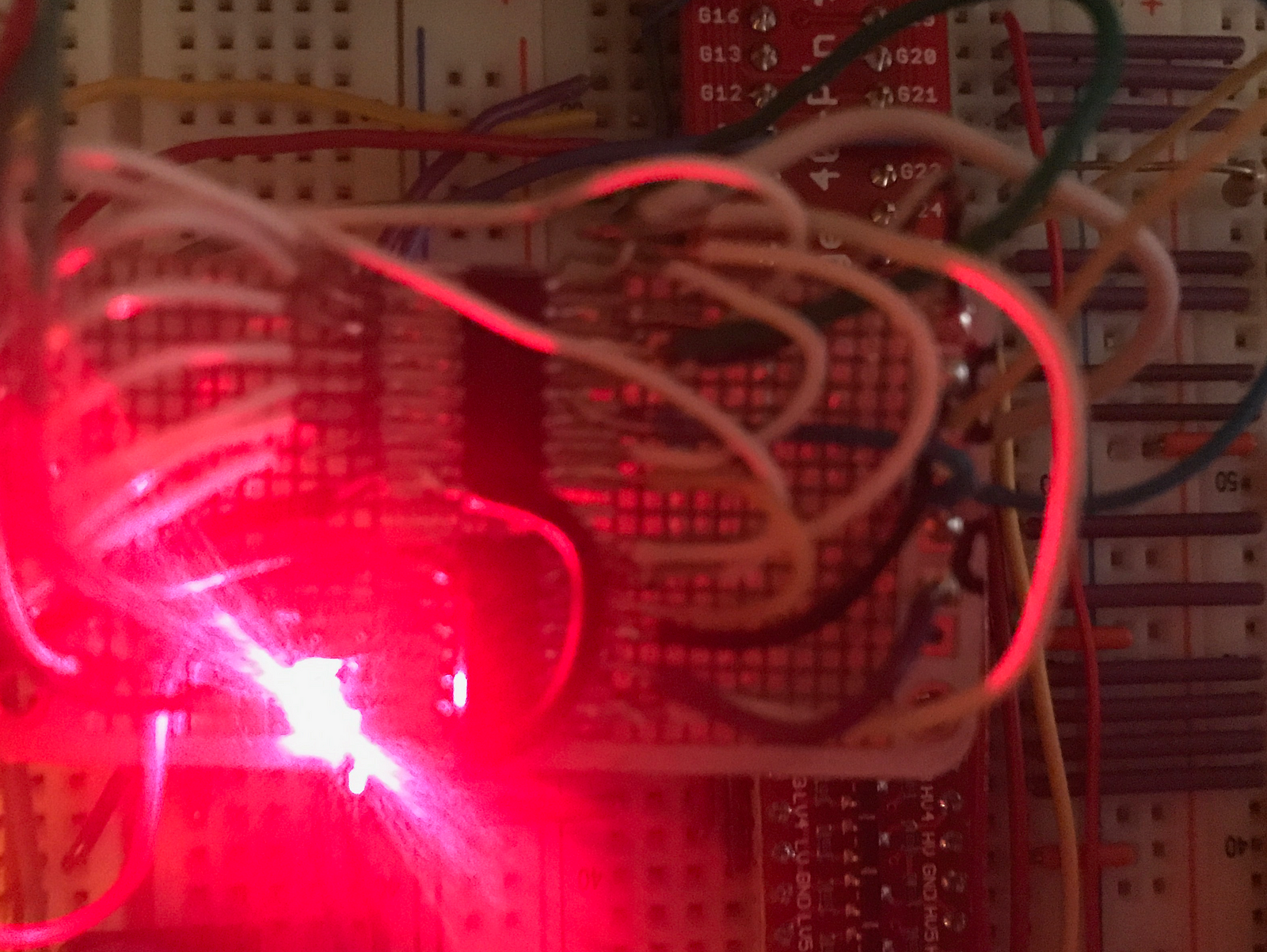
There were two shift register outputs unused, I left one disconnected, and wired up (through another 330 Ω resistor) a red LED, a LiteOn LTST-C191KRKT clear 0603, just for fun. This LED is on the PCB, not part of the 7-segment display itself. Overwhelmingly bright for its size:
Symbol encoding
Now it is a simple matter of writing the software to display each digit. Or other symbol, there’s only so much you can display with 7-segment displays, but hexadecimal is easily displayed in mixed upper/lowercase. Wikipedia has this comprehensive graphic of all 128 possible states:
I programmed 0–9 digits, and various symbols and letters:
But how can we display different symbols on each group? The anodes for each segment are shared by all groups, and cannot be powered individually. The solution is exploiting persistence of vision, rapidly switching between each group and displaying the correct digit faster than you can notice.
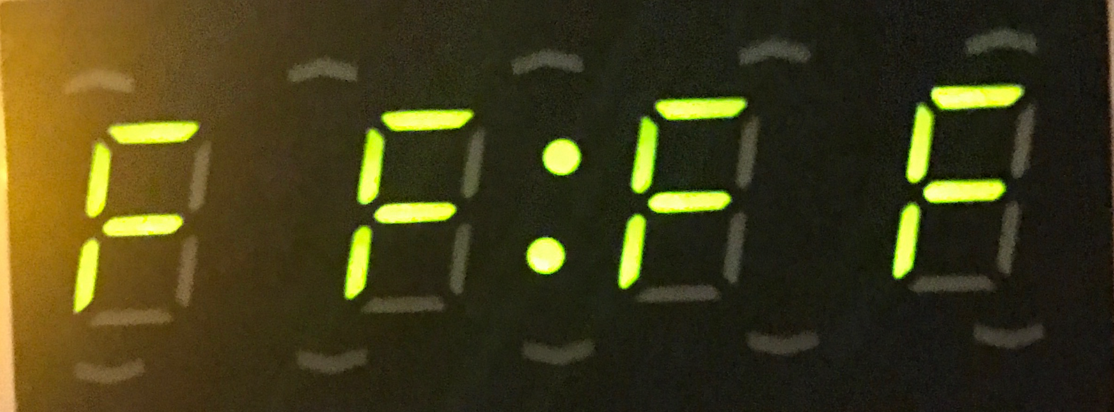
First attempt, trying to display “beef”:
You can almost make it out, but with difficulty since the other segments are illuminated albeit briefly as the bits are shifted in.
Output enable/disable vs persistence of vision
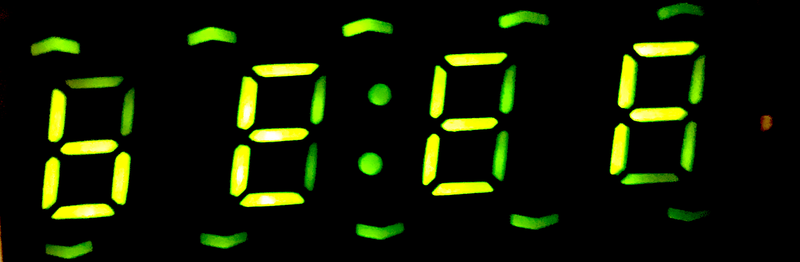
To improve readability, I wired up the “output enable” input of both shift registers to another Raspberry Pi GPIO port, G24, physical pin #18. The output is turned off when the data is being shifted in, then turned on immediately after, so no intermediate data is shown — only the segments you want to light up are lit up. Looks a lot better, here’s the beef:
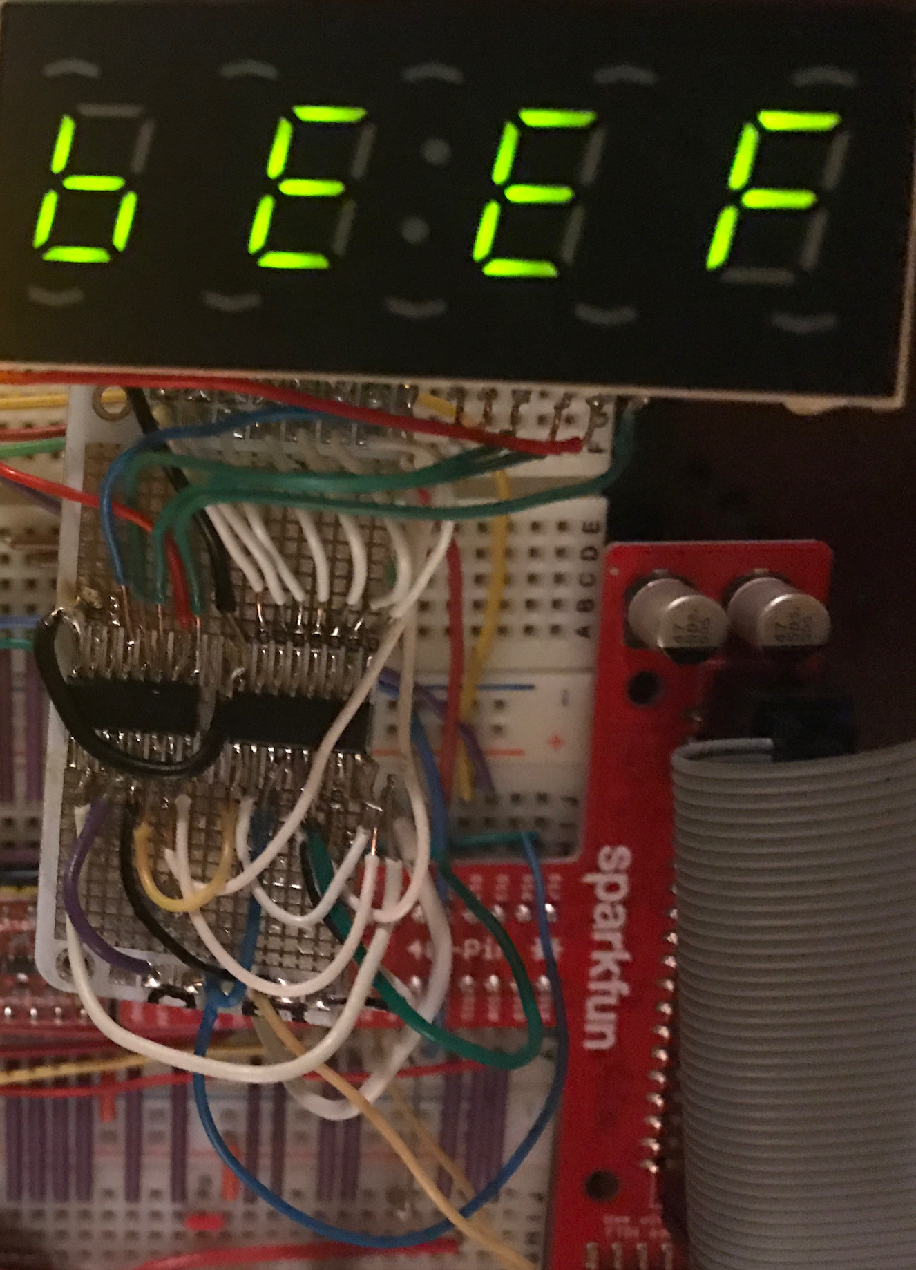
The display is even more visually distinctive in person. With a time.sleep(0.001) between setting each group, you can’t even see any blinking at all.
The output enable/disable line does require another GPIO port on the Raspberry Pi, bringing the total to 3 GPIO’s (serial data in, clock, output enable), but it is worth it. Not bad for sixteen possible parallel outputs.
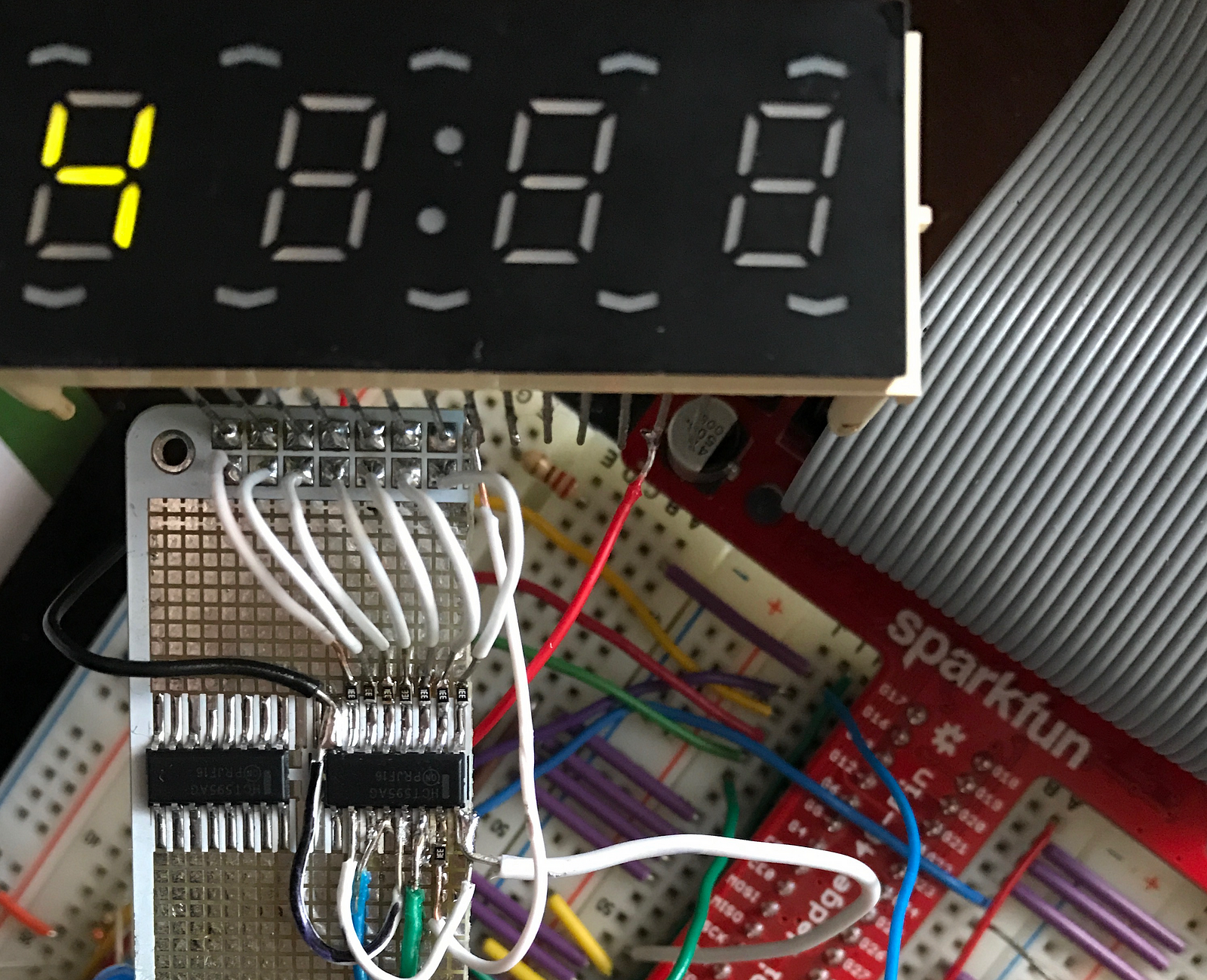
Clock display
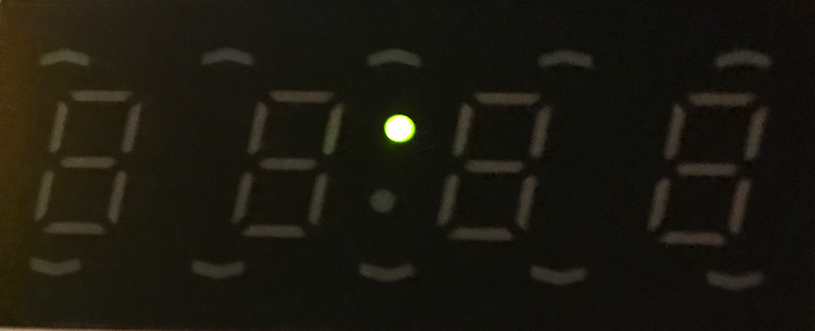
Coding up a script to set the LED display to the current time is straightforward. The only gotcha was I had to change the timezone on the Raspberry Pi by running tzselect, then adding the TZ variable to the startup script, otherwise it is set to UTC. Anyways, with some scripting we now have a digital clock, complete with a blinking center colon each second:


Micro LED
XO___XO XXX 10001 + 10 LED Circuits and Projects

Also go through the comment of each LED circuit , so as to get a better understanding of the IC’s used and the modifications that can be brought to the circuit.
The circuit uses a 555 timer and a CD 4017 IC. The clock pulses for the CD 4017 IC are provided by the timer IC which is connected as an astable multivibrator. The pin number 14 of the CD 4017 IC is the clock input pin. When the clock pulses are fed to this pin, the 10 output pins become high one by one alternatively. When the LED’s are connected to these outputs, they also continuously turn ON and OFF according to the pulses the timer provides. Take a look at the circuit diagram in the main article.
As the name implies, this circuit is used to make your home secure by automatically switching on a light around two hours after midnight. This is done with the help of a CMOS IC 4060. The circuit will need an LDR, TRIAC, LED’s and resistors from its design. Read more about this interesting circuit from its original content.
In this circuit design, the LED connected to the output glows only after a preset time after the power is switched ON. The capacitor plays an important role in switching the transistor ON. A preset and potentiometer is also needed for the circuit.
A MX 66o CMOS type voltage converter IC is used to make this LED torch circuit. The IC has the capacity to drive 3 bright white LED’s. This is a simple LED torch circuit based on IC MAX660 from MAXIM semiconductors. The MAX 660 is a CMOS type monolithic type voltage converter IC. The IC can easily drive three extra bright white LEDs. The LEDs are connected in parallel to the output pin 8 of the IC.
The circuit is nothing but two LEDs (D1 and D2), whose status are controlled by the temperature of the surroundings. A temperature sensor called Lm 35 IC is used in this circuit. With every 1 degree rise in temperature, the output the sensor increases by 10 millivolts. An op-amp called CA3130 also used and the output of the temperature sensor is given to the non-inverting input of the op-amp. The inverting input is given a reference voltage with the help of a potentiometer. When the reference voltage and the non-inverting input voltage become the same due to increase in temperature, the output of the op-amp goes into saturation. This makes the transistor connected to the output of the op-amp ON, and thus causes the LED to glow. Further working of the article can be obtained from the main link above.
This is a practical USB powered lamp circuit that can be used to light up your room during power failure. The voltage required for the working is obtained from the 5 volt available in the USB port. The voltage has to be passed through a current limiting resistor and a transistor. In the circuit two LED’s are used for the lamp. Another LED is needed as an indicator to show the connection between USB port and the circuit.
A sensor called LM 34 IC and a bar graph driver IC called LM 3914 IC are used to design a high precision LED bar graph Fahrenheit thermometer. The circuit is used to find the temperature in Fahrenheit. This can be modified to measure the temperature in degree Celsius by exchanging the LM 34 sensor IC with LM 35. A voltmeter is used to calibrate the circuit. The detailed explanation of the circuit can be obtained from the circuit above.
This single article contains three emergency light circuits made with 3 different IC’s. The first one is the Simple Emergency Light Circuit that is used to sense daylight and thus turn OFF. The reverse also happens, where the lack of daylight causes the LED to turn ON. The circuit uses an LDR to sense the light. A photograph of the circuit and the PCB design is also available in the original content.
The next article is the automatic LED emergency light circuit using the IC LM 317. The modified version is also available here.
This circuit can be used to detect the level of any conductive, non-corrosive liquids. The circuit requires five transistors and its corresponding driving LED. The transistor turns ON when the base current is supplied from the electrode probes that are connected inside the tank. Different probes are connected at different levels of the tank. One electrode probe is (F) with 6V AC is placed at the bottom of tank. All the other probes are placed at quarterly, half, and three quarterly levels. The circuit is connected in such a manner that when the water touches each level probe, the LED corresponding to it begins to glow, showing the correct level. Learn more about the circuit from the link above. Do not forget to go through the notes where the importance of pure ac for the circuit is specified.
This is the cheapest and less power consuming circuit (3 volt button cells are enough) out of the lot. The circuit is designed to work as an LED flasher to produce a rotating effect when the LED’s are arranged properly. The circuit consist of a 555 timer connected as an astable multivibrator with a duty cycle of 50 percent and 4 Hertz frequency so as to drive 6 LED’s. Another timer circuit is also connected as a trigger pulse inverter so as to drive another 6 LED’s. The circuit is arranged such that the ICs sink the current consumed by the LEDs. The detailed explanation and circuit diagram is available in the above post.
This is one of the most reliable circuits in this site. The circuit uses a 555 timer IC, six transistors, a relay, and a few passive components. The circuit is constructed in such a manner that it automatically switches the motor to OFF position as soon as the water rises above the desired level. The circuit can also be used to start the motor to pump the water into the tank. Four probes are used in the circuit which is connected on the bottom level, half level, medium level, and the full tank level. The water level is sensed using three transistors. The transistors remain off as long as the water level does not exceed more than the quarter level. When the water level touches one of the probes (other than the bottom level one), the corresponding transistors get biased and switches ON. Further working of the relays that are connected to the transistors, and the importance of the 555 timer can be understood from the main article.
This simple LED circuit is based on converting a broken or dysfunctional CFL into a LED based power saving light. The images of the completed circuit and the circuit diagram are also provided in the main article. Do not forget to look at the different procedures listed to assemble the circuit.
How a LED works – Light Emitting Diode working
A light emitting diode (LED) is known to be one of the best optoelectronic devices out of the lot. The device is capable of emitting a fairly narrow bandwidth of visible or invisible light when its internal diode junction attains a forward electric current or voltage. The visible lights that an LED emits are usually orange, red, yellow, or green. The invisible light includes the infrared light. The biggest advantage of this device is its high power to light conversion efficiency. That is, the efficiency is almost 50 times greater than a simple tungsten lamp. The response time of the LED is also known to be very fast in the range of 0.1 microseconds when compared with 100 milliseconds for a tungsten lamp. Due to these advantages, the device wide applications as visual indicators and as dancing light displays.
We know that a P-N junction can connect the absorbed light energy into its proportional electric current. The same process is reversed here. That is, the P-N junction emits light when energy is applied on it. This phenomenon is generally called electroluminance, which can be defined as the emission of light from a semi-conductor under the influence of an electric field. The charge carriers recombine in a forward P-N junction as the electrons cross from the N-region and recombine with the holes existing in the P-region. Free electrons are in the conduction band of energy levels, while holes are in the valence energy band. Thus the energy level of the holes will be lesser than the energy levels of the electrons. Some part of the energy must be dissipated in order to recombine the electrons and the holes. This energy is emitted in the form of heat and light.
The electrons dissipate energy in the form of heat for silicon and germanium diodes. But in Galium- Arsenide-phosphorous (GaAsP) and Galium-phosphorous (GaP) semiconductors, the electrons dissipate energy by emitting photons. If the semiconductor is translucent, the junction becomes the source of light as it is emitted, thus becoming a light emitting diode (LED). But when the junction is reverse biased no light will be produced by the LED, and, on the contrary the device may also get damaged.
The constructional diagram of a LED is shown below.
- LED Construction

All the semiconductors listed above can be used. An N-type epitaxial layer is grown upon a substrate, and the P-region is produced by diffusion. The P-region that includes the recombination of charge carriers is shown is the top. Thus the P-region becomes the device surface. Inorder to allow more surface area for the light to be emitted the metal anode connections are made at the outer edges of the P-layer. For the light t be reflected as much as possible towards the surface of the device, a gold film s applied to the surface bottom. This setting also enables to provide a cathode connection. The reabsorption problem is fixed by including domed lenses for the device. All the wires in the electronic circuits of the device is protected by encasing the device. The light emitted by the device depends on the type of semiconductor material used. Infrared light is produced by using Gallium Arsenide (GaAs) as semiconductor. Red or yellow light is produced by using Gallium-Arsenide-Phosphorus (GaAsP) as semiconductor. Red or green light is produced by using Gallium-Phosphorus (GaP) as semiconductor.
LED Circuit Symbol
The circuit symbol of LED consists of two arrow marks which indicate the radiation emitted by the diode.
- LED Circuit Symbol

LED Characteristics
- LED Characteristics

The forward bias Voltage-Current (V-I) curve and the output characteristics curve is shown in the figure above. The V-I curve is practically applicable in burglar alarms. Forward bias of approximately 1 volt is needed to give significant forward current. The second figure is used to represent a radiant power-forward current curve. The output power produced is very small and thus the efficiency in electrical-to-radiant energy conversion is very less.
The figure below shows a series resistor Rseries connected to the LED. Once the forward bias of the device exceeds, the current will increase at a greater rate in accordance to a small increase in voltage. This shows that the forward resistance of the device is very low. This shows the importance of using an external series current limiting resistor. Series resistance is determined by the following equation.
Rseries = (Vsupply – V)/I
Vsupply – Supply Voltage
V – LED forward bias voltage
I – Current

LED Circuit
The commercially used LED’s have a typical voltage drop between 1.5 Volt to 2.5 Volt or current between 10 to 50 milliamperes. The exact voltage drop depends on the LED current, colour, tolerance, and so on.
LED as an Indicator
The circuit shown below is one of the main applications of LED. The circuit is designed by wiring it in inverse parallel with a normal diode, to prevent the device from being reverse biased. The value of the series resistance should be half, relative to that o f a DC circuit.

LED as an Indicator
LEDS displays are made to display numbers from segments. One such design is the seven-segment display as shown below. Any desired numerals from 0-9 can be displayed by passing current through the correct segments. To connect such segment a common anode or common cathode cathode configuration can be used. Both the connections are shown below. The LED’s are switched ON and OFF by using transistors.
Advantages of LED’s
- Very low voltage and current are enough to drive the LED.
- Voltage range – 1 to 2 volts.
- Current – 5 to 20 milliamperes.
- Total power output will be less than 150 milliwatts.
- The response time is very less – only about 10 nanoseconds.
- The device does not need any heating and warm up time.
- Miniature in size and hence light weight.
- Have a rugged construction and hence can withstand shock and vibrations.
- An LED has a life span of more than 20 years.
Disadvantages
- A slight excess in voltage or current can damage the device.
- The device is known to have a much wider bandwidth compared to the laser.
- The temperature depends on the radiant output power and wavelength.
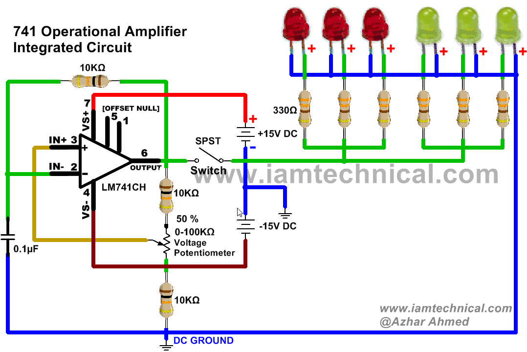
RGB LED Panel Driver
Interface a SparkFun or Adafruit 32x32 RGB LED panel to a BeagleBone Black board using the Xilinx Spartan 6 LX9 FPGA on the LogiBone FPGA board. The hardware for this project is relatively easy to construct—just 16 data signals connect the LED panel to the LogiBone FPGA board. The complexity of this project lies mostly in the RTL and software.
A demonstration of the project is available on YouTube.
A demonstration of the project expanded to six panels is also available on YouTube.
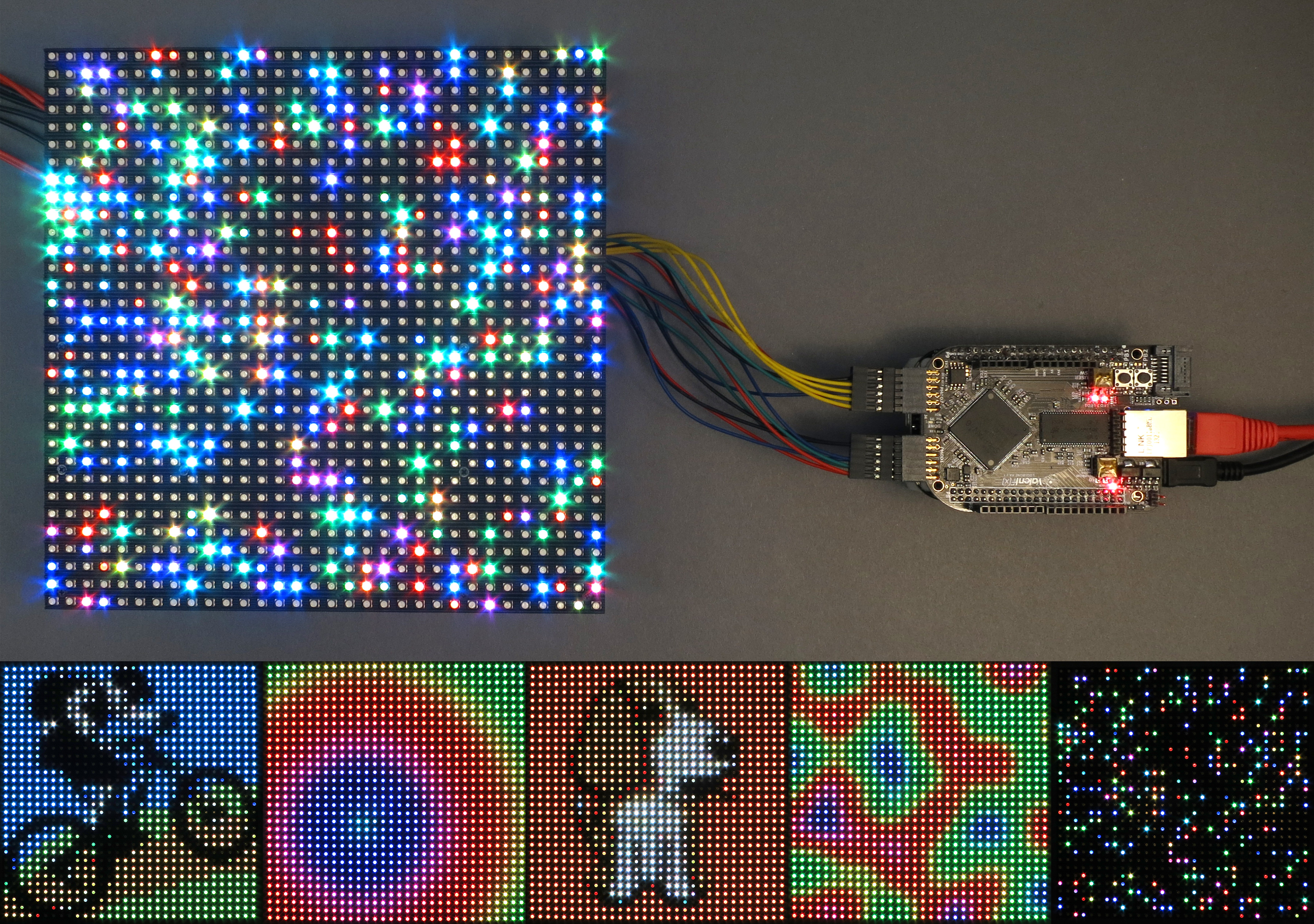
Figure 1. RGB LED panel with a random twinkling pattern connected to the LogiBone FPGA board and some other sample panel images.
Required Hardware
The following hardware items are required:
- SparkFun or Adafruit 32x32 RGB LED panel
This panel contains 1024 RGB LEDs arranged in a 32x32 matrix. The columns are driven using multiple sets of shift registers and the rows are driven, two rows at a time, using a 4-bit address decoder. The panel is driven at 1/16th duty cycle and must be continuously refreshed to display an image. - BeagleBone Black CPU board w/ USB or +5VDC power supply
You’ll need a BeagleBone Black CPU board and a +5VDC power supply for it. You can either use a USB cable to power the board from your computer or a USB power adapter or use a separate +5VDC, 2.1mm I.D., center-positive AC adapter. - LogiBone FPGA board
The FPGA board contains a Xilinx Spartan 6 LX9 FPGA. The FPGA contains 32 18kbit block RAMs. We’ll use two of the block RAMs as frame buffers to hold the RGB pixel values to be displayed on the panel. The two Digilent PMOD-compatible connectors will be used to connect to the LED panel. - Jumper wires or PMOD-to-display adapter board to connect the FPGA to the display
Initially, I used male-to-female jumper wires to connect the panel. This allowed me to connect the LogiBone FPGA board directly to the LED display panel without using the ribbon cable included with the display. If you only have male-to-male jumper wires, you’ll need to use the 16-position ribbon cable included with the display as an adapter to connect to the male pins on the display end of the jumper wires.
A much cleaner, long-term solution is to use this board and the 16-position ribbon cable included with the LED panel to make the connection from the LogiBone FPGA board to the display’s input connector. I also used precrimped terminal wires and housings to connect the FPGA and panel together. I didn’t like this solution because the precrimped terminal wires, when installed in a 2x8 housing connector, required too much force to insert onto and remove from the display’s data connector. - +3.3V power supply, 2.0A nominal, 4.0A peak
During normal operation, the display will draw at most about 2A of current. If you “stall” the refresh with an all-white pattern displayed, the two rows that are lit will draw about 3.8A. A small 3.3V, 3.0A desktop power supply such as this one from Mouser will be sufficient during normal operation. You will need to supply your own IEC60320 C13 power cord to use with this adapter.
These panels can also be run from +5V instead of 3.3V. You will get brighter greens, brighter blues, and less-red whites if driven from +5V instead of +3.3V. You'll also pull about 15% more current and use about 65% more power at +5V instead of +3.3V. If you use a +5V supply, be extra careful not to accidently connect the LogiBone FPGA board to the display’s output connector. - Female DC barrel jack adapter (optional)
A female DC barrel jack adapter will make connecting the panel to the power supply much easier. If you don’t have an adapter, you can always cut, splice, solder, and heat shrink the connections between the power supply and led panel.
Required Software
- Stock ValentFX LogiBone Ubuntu build w/ the LogiBone logibone_<revision>_dm.ko kernel module and logi_loader
Download and follow the instructions here to install the default LogiBone Ubuntu image on an SD card. - Xilinx ISE WebPack Software
If you want to build the FPGA bit file yourself or customize the Verilog to drive more panels or add other custom functionality (such as a coprocessor to help compute difficult pixel patterns), you’ll need to download and install the Xilinx ISE WebPack software. Instructions are here. If you only want to use the default FPGA bit file, you can skip installing the Xilinx ISE WebPack software. - Glen’s LED panel GIT repository
Finally, you’ll need to clone my GIT repository at http://github.com/bikerglen/beagle to your BeagleBone Black. This repository contains the Verilog source code for the FPGA, a prebuilt bit file, and C++ source code for displaying some demonstration patterns on the panel. Instructions for downloading or cloning and using the repository are presented later.
Theory of Operation
This system has three major components: the LED panel, the FPGA code, and the C++ code. Let’s examine each of these three major components in detail.
The LED Panel
LED Panel Hardware
The LED panel contains 1024 RGB LEDs arranged in a matrix of 32 rows and 32 columns. Each RGB LED contains separate red, green, and blue LED chips assembled together in a single package. The display is subdivided horizontally into two halves. The top half consists of 32 columns and 16 rows. The bottom half also consists of 32 columns and 16 rows.
The display’s columns are driven by one set of drivers and the display’s rows are driven by another set of drivers. To illuminate an LED, the drivers for both the column and the row for that LED must be turned on. To change the color of an LED, the red, green, and blue chips in each LED package are controlled individually and have their own column drivers. Figure 2 below is a schematic representation of the display’s column and row driver organization.
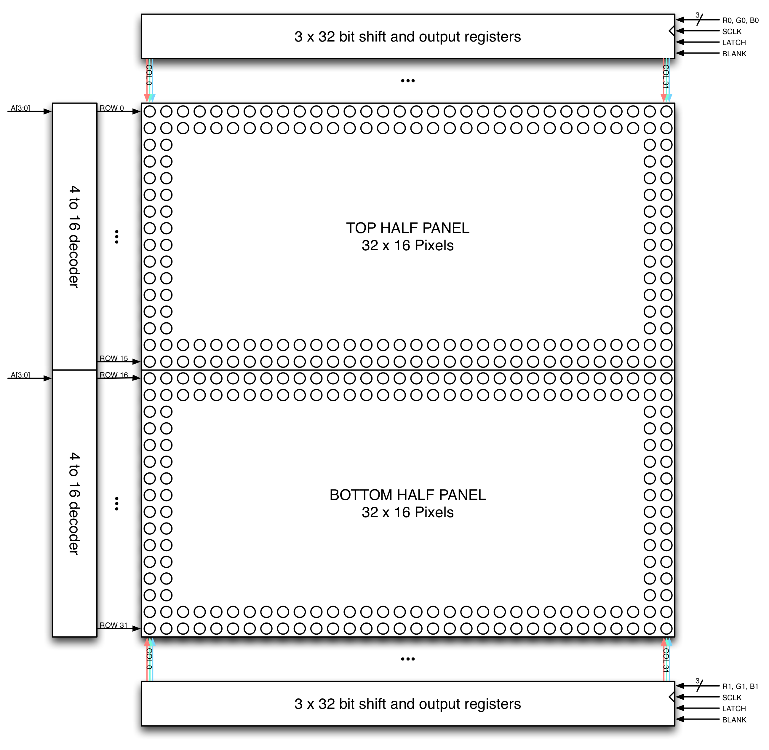
Figure 2. RGB LED panel column and row driver organization.
The panel contains six sets of column drivers; three for the top half of the display and three for the bottom. Each driver has 32 outputs. The three drivers for the top of the display drive the red, green, and blue chips in each of the 32 columns of LEDs in rows 0 to 15 of the panel. The three drivers for the bottom of the display drive the red, green, and blue chips in each of the 32 columns of LEDs in rows 16 to 31 of the panel.
Each of the drivers has a serial data input, a blanking input, a shift register, and a parallel output register as shown below in Figure 3. The data present on the serial data input is shifted into the shift register using the SCLK signal. After an entire row of data has been shifted in to the shift register, the LATCH signal is used to transfer the row of pixel data from the shift register into the parallel output register. If a bit in the output register is a ‘1’ and the blanking input is deasserted, the driver for that column will be enabled; otherwise, the driver will be turned off. Data is shifted from the right edge of the display to the left edge of the display. In other words, the first bit shifted in will be displayed on the left edge of the display and the last bit shifted in will be displayed on the right.
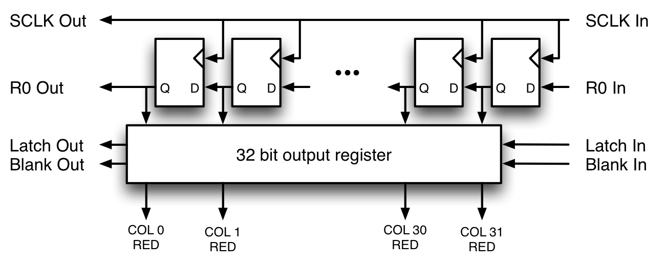
Figure 3. Column driver operation for the R0 data input and top-half red columns outputs. There are two more of these shift registers at the top of the display for the top-half green and blue columns and three more at the bottom for the bottom half red, green, and blue columns.
The red, green, and blue column drivers for the top half of the display are attached respectively to the R0, G0, and B0 data inputs. The red, green, and blue column drivers for the bottom half of the display are attached respectively to the R1, G1, and B1 data inputs. All six of the 32-bit drivers share common SCLK, LATCH, and BLANK signals.
The rows are driven using four address bits and an address decoder. The four-bit address input to the row drivers is decoded and the two row drivers corresponding to that address will be turned on. When A[3:0] is 0, rows 0 and 16 of the display are turned on. When A[3:0] is 1, rows 1 and 17 of the display are turned on. This pattern continues until A[3:0] is 15 and rows 15 and 31 are turned on.
In addition to the row and column logic and drivers, the display has a blanking input. This input is most likely connected to the column drivers. When the blanking signal is asserted, all of the pixels are turned off and the display will be black. When the blanking signal is deasserted, the addressed rows and columns will be driven and the corresponding pixels illuminated. To display an image without flickering and ghosting, all of these signals must be used and properly sequenced when driving the panel.
Driving the Panel
The display is multiplexed and has a 1/16th duty cycle. This means that no more than one row out of the 16 in the top half of the display and one row out of the 16 in the bottom half of the display are ever illuminated at once. Furthermore, an LED can only be on or off. If both the row and column for an LED are turned on, the LED will be illuminated; otherwise, the LED will be off.
To display an image, the entire LED panel must be scanned fast enough so that it appears to display a continuous image without flickering. To display different colors and different brightness levels, the brightness of the red, green, and blue LED chips within each LED package must be adjusted by varying the amount of time that each LED chip is on or off within a single refresh cycle.
The basic process used to refresh the display when using three bits-per-pixel color (one bit for red; one bit for green; and one bit for blue) is the following:
- Shift the pixel data for row 0 into the top column drivers and the pixel data for row 16 into the bottom column drivers using the R0, G0, B0, R1, G1, and B1 data inputs and the SCLK shift clock signal.
- Assert the blanking signal to blank the display.
- Set the address input to 0.
- Latch the contents of the column drivers‘ shift registers into the column drivers‘ output registers using the LATCH signal.
- Deassert the blanking signal to display rows 0 and 16.
- Wait some fixed amount of time.
- Repeat the process for each of the pairs of rows in the display.
- Repeat the entire process at least 100 to 200 times per second to prevent flicker.
The above process uses one bit per LED color. This will give you eight possible colors: black; the primary colors red, green, and blue; the secondary colors cyan, magenta, and yellow; and white.
To display more colors and brightness levels the above technique is modified to use binary coded modulation. In binary coded modulation, each pixel is controlled using more than a single bit per color per pixel. The amount of time each red, green, and blue LED chip is on is then varied proportionally to the pixel’s red, green, and blue values.
In binary coded modulation, the following process is performed to refresh the display:
- Shift bit zero of each pixel’s red, green, and blue values for rows 0 and 16 into the column drivers.
- Assert the blanking signal to blank the display.
- Set the address input to 0.
- Latch the contents of the column drivers‘ shift registers into the column drivers‘ output registers using the LATCH signal.
- Deassert the blanking signal to display rows 0 and 16.
- Wait some amount of time, N.
- Repeat the above process for the next higher order bit of color data in the same row. In step 6, wait two times the previous delay time. Repeat this process for each bit of color data, doubling the delay time after displaying each successive bit.
- Repeat the above process for each of the pairs of rows in the display.
- Repeat the entire process at least 100 to 200 times per second to prevent flicker.
Note that in actual implementations, the process of shifting the pixel data into the shift registers in Step 1 is usually done during the wait time in Step 6.
Global display dimming can be performed by varying the amount of time the blanking signal is asserted or deasserted within the wait time period, N. For example, asserting the blanking signal 25% early will result in a display with a brightness of 75% instead of 100%. Note that during global dimming, the wait time itself is not shortened or lengthened; only the blanking signal is modified to be asserted earlier than it normally would be.
The FPGA
The FPGA interfaces the C++ pattern generation software running on the BeagleBone Black CPU to the LED panel. The FPGA does the heavy lifting required to refresh the entire LED panel about 200 times per second. This leaves the BeagleBone Black CPU free to generate the patterns and perform other tasks.
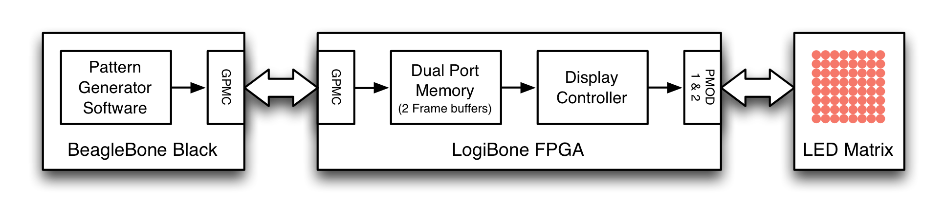
Figure 4. Block diagram of the system including a block diagram of the FPGA’s major functional blocks.
As shown in Figure 4 above, software running on the BeagleBone Black generates patterns. These patterns are fed to the FPGA on the LogiBone board using the TI SOC’s GPMC bus. These patterns are written to a dual-port memory that serves as a display buffer. Finally a display controller reads the patterns out of the dual port memory, shifts the data into the display, and enables the row drivers as needed to display the image. The entire process is repeated about 200 times per second and generates a 32 x 32 RGB image with 12-bit color without any interaction from the BeagleBone Blacks’ CPU.
GPMC Interface
The TI SOC has a programmable memory interface called the general-purpose memory controller (GPMC). This interface is extremely flexible. It can operate in both synchronous and asynchronous modes and the bus timing is programmable in 10ns increments. The GPMC bus will be used to transfer pixel data from the software on the BeagleBone Black to the FPGA on the LogiBone board.
In our system, the GPMC is configured to operate in its asynchronous, multiplexed address/data mode. In this mode, both the address and data buses are 16 bits wide. This permits an entire 12-bit pixel to be transferred from the CPU on the BBB to the FPGA on the LogiBone board in a single write operation. For more information on the GPMC’s asynchronous, multiplexed mode of operation, see sections 7.1.3.3.10.1.1 of the AM335x ARM® Cortex™-A8 Microprocessors Technical Reference Manual.
I’m using a slightly different circuit in the FPGA to interface to the GPMC bus than the stock LogiBone projects. It’s a bit slower than the stock VHDL circuit, but guarantees that each write from the CPU over the GPMC bus creates exactly one write strobe pulse to the register interface inside the FPGA. Because it’s slightly slower than the stock circuit, it requires modified bus timing and thus a custom device tree setup file. Figure 5 below shows the bus timing using the modified GPMC interface to perform a write to the FPGA. Figure 6 below shows the bus timing using the modified GPMC interface to perform a read from the FPGA.
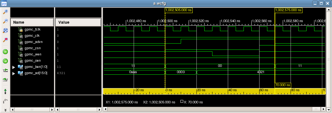
Figure 5. Simulation of a write to the GPMC target using the modified bus timings.
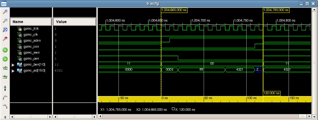
Figure 6. Simulation of a read from the GPMC target using the modified bus timings.
The read or write address is latched into a temporary holding register on the rising edge of the GPMC_ADVN signal and the write data is latached into its own temporary holding register on the falling edge of the GPMC_WEN signal. This requires using the GPMC_ADVN and an inverted version of the GPMC_WEN data signals as clocks. Technically, using data signals as clocks is gross. It’s actually so gross, the Xilinx tools will generate an error for this condition. But you can set an exception in the UCF file for the affected nets and force synthesis to continue. It would be much better to use the GPMC in its synchronous mode, but this technique is good enough for an FPGA until I have time to build a synchronous version of the interface, a synchronous GPMC bus model for simulation, and learn how to modify the device tree further.
In addition to latching the address and write data values into holding registers, the GPMC_CSN, GPMC_WEN, and GPMC_OEN controls signals are registered and brought into the FPGA’s 100MHz clock domain. Once in the FPGA’s clock domain, the WEN and OEN signals are gated with the CSN signal and edge detected to detect writes to the GPCM target and reads from the GPMC target. When a read or write is detected, the contents of the address and write data holding registers are captured into registers in the FPGA’s 100MHz clock domain.
The primary reason to slow down the GPMC bus versus the stock device tree setup file was to stretch the time that each of these control signals is low or high to at least 30ns to guarantee that the edges of the signals could be detected in the FPGA’s 100MHz clock domain. This also guaranteed that the address and data would be stable in their own holding registers before moving the contents of those registers into the address and data registers that are clocked in the FPGA’s 100MHz clock domain.
The outputs of the GPMC target are a bus that I’m calling the slow bus. The slow bus connects the GPMC target to the FPGA’s register interface. Figure 7 shows an example slow bus write operation. Figure 8 shows an example slow bus read operation.
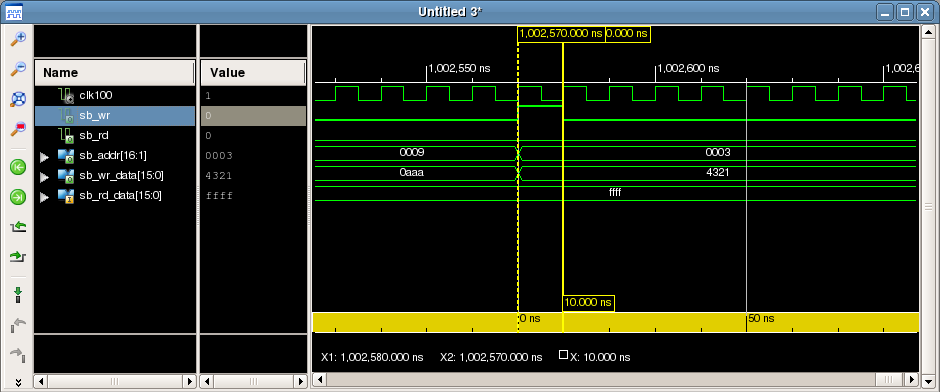
Figure 7. Simulation of a slow bus write.
sb_addr, sb_wr, and sb_wr_data will be valid for exactly a single 100MHz clock pulse every time a write occurs on the GPMC bus. When the register interface sees sb_wr asserted, it writes sb_wr_data into the register at sb_addr.
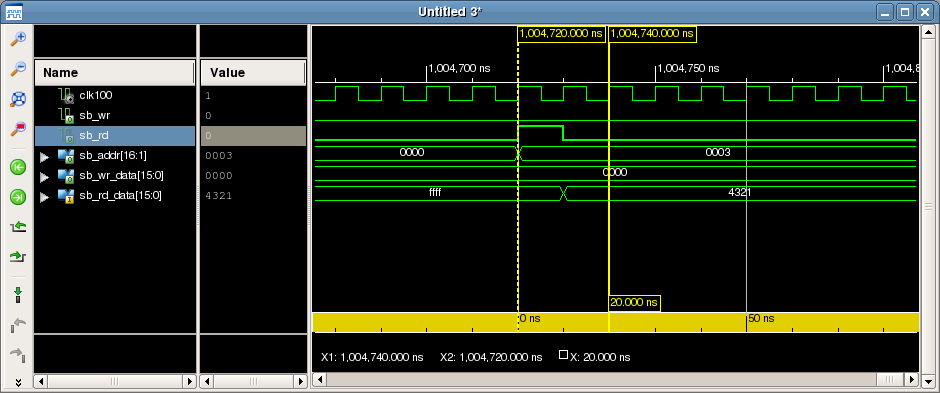
Figure 8. Simulation of a slow bus read.
sb_addr and sb_rd will be valid for exactly a single 100MHz clock pulse every time a read occurs on the GPMC bus. The register interface sees sb_rd asserted then must return the value of the register at the address sb_addr on the sb_rd_data bus on the very next clock cycle.
Register Interface
The register interface is implemented in the top level of the FPGA Verilog. The register interface defines the view the software has of the FPGA. Table 1 below lists the registers in the FPGA.
FPGA Address
|
BBB SOC Address
|
Name
|
Description
|
0x0000
|
0x0000
|
R/W Test Reg 1
|
Read / write test register. Write any value to this register. Reads return previously written value.
|
0x0001
|
0x0002
|
R/W Test Reg 2
|
Read / write test register. Write any value to this register. Reads return previously written value.
|
0x0002
|
0x0004
|
R/W Test Reg 3
|
Read / write test register. Write any value to this register. Reads return previously written value.
|
0x0003
|
0x0006
|
R/W Test Reg 4
|
Read / write test register. Write any value to this register. Reads return previously written value.
|
0x0004
|
0x0008
|
Read-Only Test Reg 1
|
Read-only test registers. Reads return hard-coded values. See RTL for returned values.
|
0x0005
|
0x000a
|
Read-Only Test Reg 2
|
Read-only test registers. Reads return hard-coded values. See RTL for returned values.
|
0x0006
|
0x000c
|
Read-Only Test Reg 3
|
Read-only test registers. Reads return hard-coded values. See RTL for returned values.
|
0x0007
|
0x000e
|
Read-Only Test Reg 4
|
Read-only test registers. Reads return hard-coded values. See RTL for returned values.
|
0x0008
|
0x0010
|
Display Buffer Address Register
|
Writes to this register set the display buffer address pointer. The display buffer address pointer points to the location in the display buffer memory that will be modified when a pixel value is written to the display buffer data register. See the display buffer section of this document for the arrangement of pixels in memory.
|
0x0009
|
0x0012
|
Display Buffer Data Register
|
Writing a pixel value to this register writes the pixel value to the display buffer at the address pointed to by the display buffer address pointer. After each write, the display buffer address pointer is incremented by one to point at the next pixel in the display buffer.
|
0x000a
|
0x0014
|
Display Buffer Select Register
|
0 selects buffer 0 for display; 1 selects buffer 1 for display; Reads return which buffer is currently being displayed.
|
Table 1. FPGA registers.
Display Buffers
The display buffers are implemented usinx Xilinx Block RAMs configured as dual-port memories with asynchronous read and write ports. The first RAM contains display buffers 0 and 1 for the top half of the display. The second RAM contains display buffers 0 and 1 for the bottom half of the display. Structuring the memories to contain half the display each permits the pixels in rows 0 to 15 to be read from memory on the exact same clock that the pixels in rows 16 to 31 are read from memory.
Display buffer 0 is located at address 0x0000. Display buffer 1 is located at address 0x0400. Each display buffer contains 1024 12-bit RGB values arranged as 32 rows of 32 columns. Within each display buffer, the top-left pixel is stored at offset 0, the bottom-right pixel is stored at offset 0x3ff. Bits 4 to 0 of the pixel offset are 0x00 for pixels in the leftmost column on the display; bits 4 to 0 of the pixel offset are 0x1F for pixels in the rightmost column.
Pixels are stored in the memory as 12-bit RGB values. These values are stored right-justiified. Bits 11 to 8 are the red pixel level, bits 7 to 4 are the green level, and bits 3 to 0 are the blue level.
Display Driver
The display driver reads pixel values from memory, shifts those values to the display, and cycles through the rows of the display as required to implement binary coded modulation as described in the theory of operation section of this document. The display driver is implemented as a state machine. Each state implements a step in the refresh process. When that step is complete, the state machine moves to the next step in the process.
Figure 9 below shows simulation waveforms for the control and data outputs for three rows worth of display data. The basic process is to blank the display, latch in the previously shifted data, update the row selects, unblank the display, shift in the next set of pixel data, and then wait for an update timer to expire. This is repeated four times for each row. If you examine the blanking output, you’ll notice that its low period doubles three times within the output period for each display row. This is the result of using binary coded modulation to vary the intensity of each pixel.
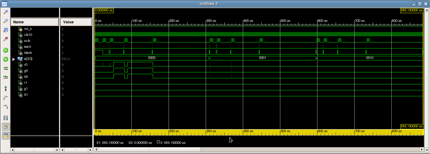
Figure 9. Simulation waveforms for the display data output connections.
The Software
The demonstration software uses the /dev/logibone_mem device to communicate with the FPGA. The driver for this device is part of the stock LogiBone Ubuntu image and its loadable kernel module is installed by the modified device tree setup shell script that’s included in the GitHub repository for the LED panel. (More on this subject in a later section.) This driver maps the registers in the FPGA to a portion of the BBB CPU’s address space using the GPMC. The GPMC normally maps memory into the CPU’s address space. Because our FPGA looks like a memory to the GPMC bus, its registers can be mapped into the CPU address space too. Pretty cool. No SPI, I2C, etc.; just fast parallel accesses between the CPU and the FPGA. This memory-mapped space can then be accessed by opening the /dev/logbone_mem device using the C library open function call and reads and writes to a register in the FPGA can be performed using the pread and pwrite C library function calls.
Figure 10 below is a block diagram of the demonstration software stack. In the demonstration software, main opens the /dev/logibone_mem device, fills the global buffer memory, gLevels, with all black, and then calls WriteLevels to write the global buffer to the display and clear the display. Once the display is cleared, the main function instantiates a pattern / animation subclass such as a radiating circle, perlin noise, or colorwash subclass. This subclass is derived from a generic pattern base class.
The generic pattern base class uses a constructor to set the height and width of the pattern to generate. Derived classes may add their own arguments to their own constructors. The base class also has two pure virtual member functions, init and next, that any derived classes must implement. The init function prepares a pattern to be displayed for the first time. It typically resets any state information back to the start of the pattern. The next function calculates the next frame of the pattern and writes that frame to the global gLevels buffer.
After main has instantiated the pattern subclass, it calls the subclass’s init funciton. Main then installs a timer that executes at 50Hz and goes to sleep. When the timer expires, a timer handler function is called. The timer handler function calls WriteLevels to write the previously computed frame in gLevels to the next available display buffer in the FPGA and makes that display buffer active. The writes to the FPGA display buffers are performed using the registers documented in the Register Interface section of this document.
After WriteLevels has completed, the timer handler function calls the pattern’s next member function. The next function generates the next frame in the animation, writes that frame to gLevels, and returns—without calling WriteLevels. The timer handler then sleeps until the next time the timer expires. By calling WriteLevels before calling next, the amount of time between displayed frames will not vary even if the amount of time that next takes to execute varies between frames.
In order for animations to run smoothly, the timer handler function must complete execution before the timer expires next. This means that each frame in the animation must take less than roughly 20ms to compute.
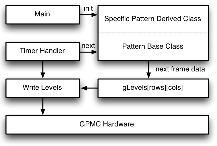
Figure 10. Block diagram of the demonstration software stack.
Connecting the Hardware
The display requires only a data connection to the LogiBone FPGA board and a power connection to a +3.3V power supply to operate. These connections are detailed in the sections below.
Display Data Connections
Figure 11 below lists the connections between the PMOD connectors and the display’s data input connector. You will need to make 16 connections total between the LogiBone board and the display panel. Thirteen of these are data connections; three of these are grounds. You can either use jumper wires or the PMOD-to-display adapter board. If you use jumper wires, the wiring will look something like Figure 12. With the adapter board, it will look something like Figure 13. Note that the PMOD connectors’ pins are numbered differently than double row headers are normally numbered.
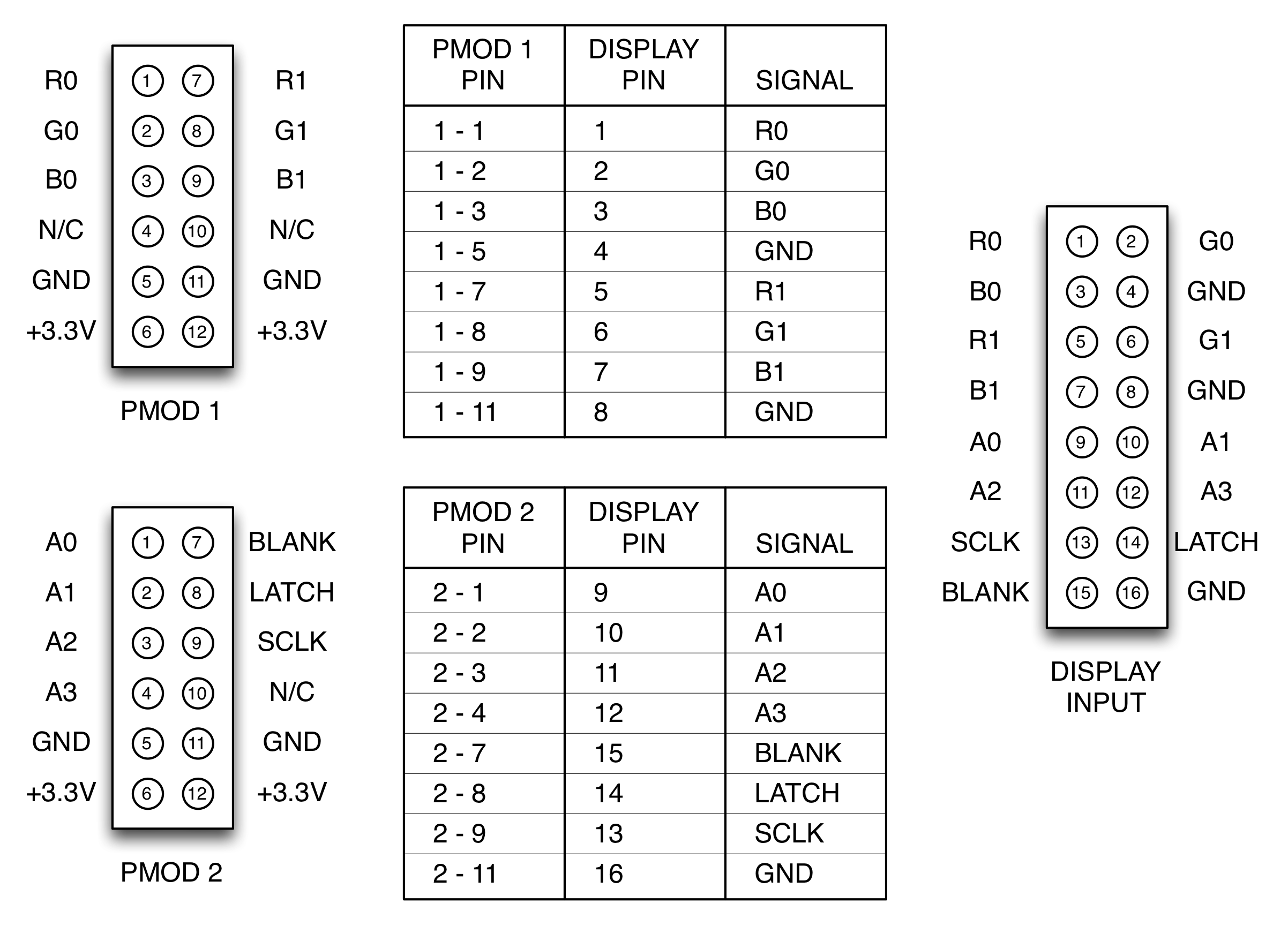
Figure 11. PMOD connector pin outs, connections between the PMOD connectors and the display input connector, and the display connector pin out.
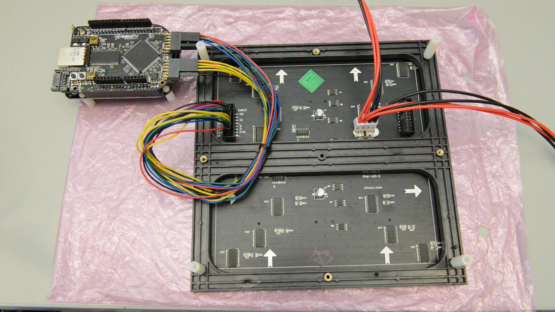
Figure 12. LogiBone FPGA board connected to RGB LED panel using jumper wires.
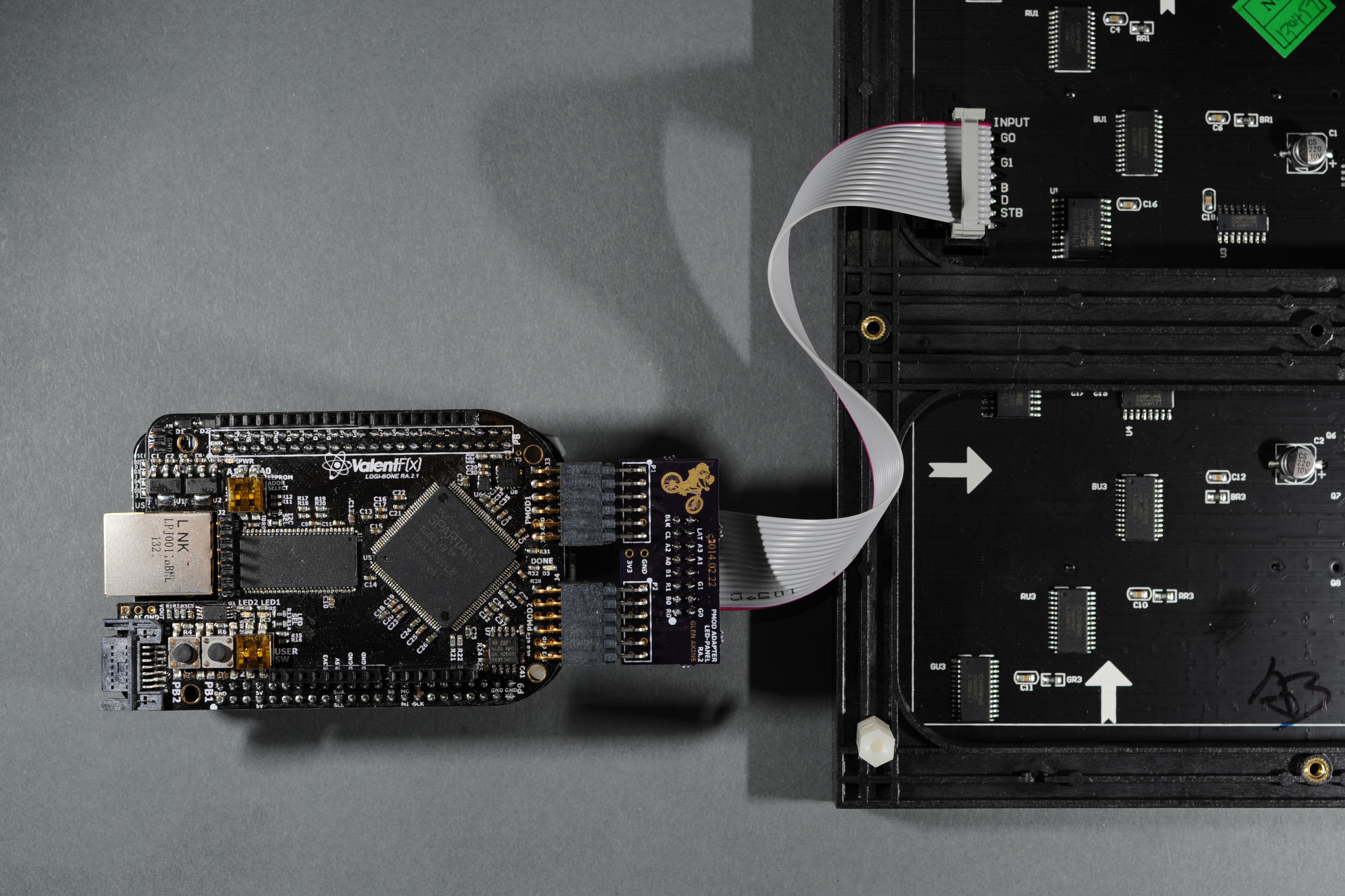
Figure 13. LogiBone FPGA board connected to RGB LED panel using the PMOD-to-display adapter board.
Display Power Supply Connection
Once the data signals have been connected, make the power supply connection to the display. Figure 14 below shows the basics. Using the DC barrel jack adapter, connect the positive terminal of the power supply to the red wire of the wire harness and connect the negative terminal of the power supply to the black wire of the wire harness. Before connecting the wire harness to the display, use a volt meter to verify the polarity of the connections. Once you’ve verified the polarity, disconnect the power and plug the wire harness into the display.
I left the spade lugs on the wire harness because I plan on using the display in a bigger project and don’t want to remove them until I’m sure I don’t need them in the bigger project. If you leave the spade lugs on too, be careful they don’t accidentally short to any other electronics. You might want to wrap them with electrical tape just to be sure. If you don’t need or want the spade connectors, feel free to cut them off, strip a bit of insulation off the wires, and connect them directly to the DC barrel jack adapter.
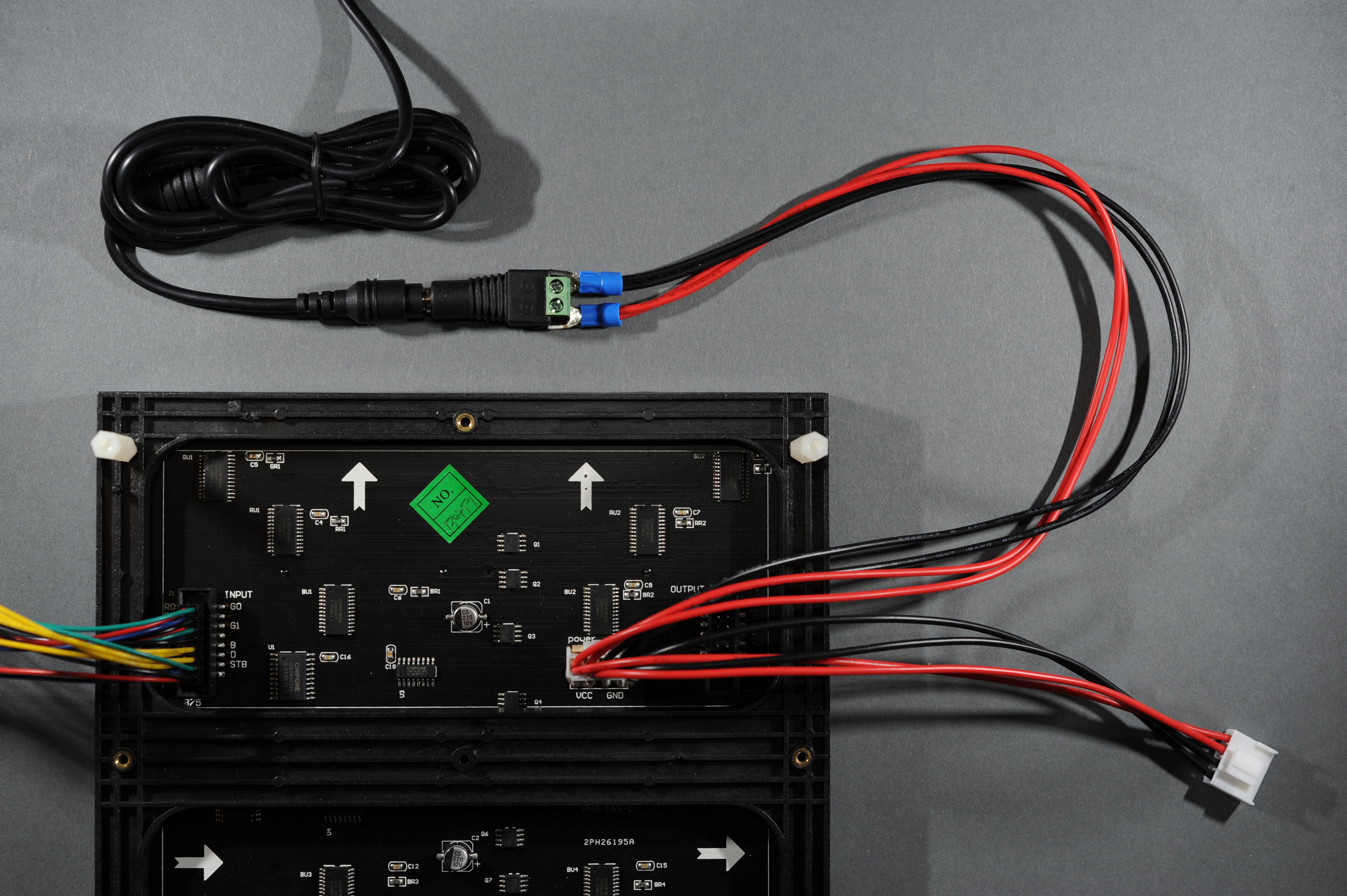
Figure 14. Connecting the power supply to the RGB LED panel using a female DC barrel jack adapter.
++++++++++++++++++++++++++++++++++++++++++++++++++++++++++++++++++
e- Animation LED Working


++++++++++++++++++++++++++++++++++++++++++++++++++++++++++++++++++++++
Tidak ada komentar:
Posting Komentar