Trigger Pulse Generator Using Proposed Buffered Delay Model and Its Application

Triggering device
A Triggering device is an electronic circuit, such as a Schmitt trigger, which is used to control another electronic circuit.
In simple language. trigger is what pushes the electronic devices from threshold (no activity) to active state.
Take a diode. There are two types of triggering, but essentially you’re reducing the bridge gap at semiconductor links, thereby allowing electrons to flow.
The same concept is taken into electronic circuits, take transient circuits, Flip-flops, PWM (most important of all).
Uses
In many of industrial operations, the delivery of a variable and controlled amount of electrical power is necessary. The most common of these operations include electric lighting, electric motor speed control, electric welding, and electric heating. Although it is always possible to control the amount of electrical power delivered to a load by using a variable transformer to create a variable secondary output voltage, these transformers are physically large and expensive and need frequent maintenance (in high power ratings). There are other methods of controlling power to a load, but they are mostly not available for high power applications.
Since 1961, an alternative method, using thyristors, has been in use. Both silicon-controlled rectifiers (SCR) and TRIACs are members of the thyristor family. The term thyristor includes all the semiconductor devices, which show inherent ON-OFF behavior, as opposed to allowing gradual changes in conduction. All thyristors are regenerative switching devices, and they cannot operate in linear manner. Thus, a transistor is not a thyristor even though it can operate like a switch (ON-OFF). The transistor is not inherently an ON-OFF device, and it is possible for a transistor to operate linearly.[1]
Some thyristors can be gated into the ON state. Other thyristors cannot be gated ON, but they can be turned ON when the applied voltage reaches a certain breakover value.
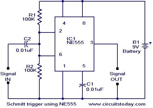
Scmitt Trigger circuit using NE 555
Apart from the timing functions ,the two comparators of the 555 timer can be used independently for other applications.One example is a Schmitt Trigger shown here. The two comparator inputs (pin 2 & 6) are tied together and biased at 1/2 Vcc through a voltage divider R1 and R2.Since the threshold comparator wil trip at 2/3 Vcc and the trigger comparator will trip at 1/3Vcc,the bias provided by the resistors R1 & R2 are centered within the comparators trip limits.
By modifying the input time constant on the circuit,reducing the value of input capacitor (C1) to 0.001 uF so that the input pulse get differentiated,the arrangement can also be used either as a bistable device or to invert pulse wave forms.In the later case ,the fast time combination of C1 with R1 & R2 causes only the edges of the input pulse or rectangular waveform to be passed.These pulses set and reset the flip-flop and a high level inverted output is the result.
Circuit diagram with Parts list.
Notes.
- Assemble the circuit on a good quality PCB or common board.
- The circuit can be powered from a 9V battery or 9V DC power supply.
- The IC NE555 could be mounted on holder.

To have control over the timing of any event (logic change) the trigger signal is used.
Edge-triggered Flip-Flops & Mono-stable multivibrators, SCR triggering by gate signal are some examples.
Trigger circuit : A circuit or network in which the output changes abruptly with an infinitesimal change in input at a predeterminedoperating point. Also known as trigger. A circuit in which an action is initiated by an input pulse, as in a radar modulator.
Schmitt trigger
Definition
Schmitt trigger is an electronic circuit with positive feedback which holds the output level till the input signal to comparator is higher than the threshold.It converts a sinusoidal or any analog signal to digital signal. It exhibits hysteresis by which the output transition from high to low and low to high will occur at different thresholds.
In electronics, a Schmitt trigger is a comparator circuit with hysteresis implemented by applying positive feedback to the noninverting input of a comparator or differential amplifier. It is an active circuit which converts an analog input signal to a digital output signal. The circuit is named a "trigger" because the output retains its value until the input changes sufficiently to trigger a change. In the non-inverting configuration, when the input is higher than a chosen threshold, the output is high. When the input is below a different (lower) chosen threshold the output is low, and when the input is between the two levels the output retains its value. This dual threshold action is called hysteresis and implies that the Schmitt trigger possesses memory and can act as a bistable multivibrator (latch or flip-flop). There is a close relation between the two kinds of circuits: a Schmitt trigger can be converted into a latch and a latch can be converted into a Schmitt trigger.
Schmitt trigger devices are typically used in signal conditioning applications to remove noise from signals used in digital circuits, particularly mechanical contact bounce in switches. They are also used in closed loop negative feedback configurations to implement relaxation oscillators, used in function generators and switching power supplies.

Comparison of the action of an ordinary comparator and a Schmitt trigger on a noisy analog input signal (U). The output of the comparator is A and the output of the Schmitt trigger is B. The green dotted lines are the circuit's switching thresholds. The Schmitt trigger tends to remove noise from the signal .
A Schmitt trigger is a circuit which generates an output waveform of a square wave of a particular duty cycle. It can be implemented on several devices, however most commonly on the operational amplifier.
When we give a positive feedback to the opamp, it no more behaves as a linear IC. If the input voltage difference (i.e Vp-Vn) is greater than 0, then it gives a +Vsat output and if the input voltage difference is lesser than 0V, it gives a -Vsat output.
This is the idea behind the Schmitt trigger. Now the output of the opamp is fed back to the non inverting terminal of the IC. This is used to control the upper and lower threshold voltages in the case of a Schmitt trigger. To vary the duty cycles, we use diodes and more resistors.
Schmitt trigger can also be done on devices like 555 timers and bipolar junction transistors (BJTs).
EDIT: After an important mention in the comments by Anusha, I would like to add that the circuit mentioned here is for the case of an inverting Schmitt trigger.
For the case of a non inverting Schmitt trigger, we feed the input to the non inverting terminal of the operational amplifier.

They x-y curve is also mentioned, the graph is the exact reverse of the one above.
Invention
The Schmitt trigger was invented by American scientist Otto H. Schmitt in 1934 while he was a graduate student,[1] later described in his doctoral dissertation (1937) as a "thermionic trigger."[2] It was a direct result of Schmitt's study of the neural impulse propagation in squid nerves.[2]
Implementation
Fundamental idea

Circuits with hysteresis are based on the fundamental positive feedback idea: any active circuit can be made to behave as a Schmitt trigger by applying a positive feedback so that the loop gain is more than one. The positive feedback is introduced by adding a part of the output voltage to the input voltage. These circuits contain an 'attenuator' (the B box in the figure on the right) and a 'summer' (the circle with "+" inside) in addition to an amplifier acting as a comparator. There are three specific techniques for implementing this general idea. The first two of them are dual versions (series and parallel) of the general positive feedback system. In these configurations, the output voltage increases the effective difference input voltage of the comparator by 'decreasing the threshold' or by 'increasing the circuit input voltage'; the threshold and memory properties are incorporated in one element. In the third technique, the threshold and memory properties are separated.
Dynamic threshold (series feedback): when the input voltage crosses the threshold in some direction the circuit itself changes its own threshold to the opposite direction. For this purpose, it subtracts a part of its output voltage from the threshold (it is equal to adding voltage to the input voltage). Thus the output affects the threshold and does not impact on the input voltage. These circuits are implemented by a differential amplifier with 'series positive feedback' where the input is connected to the inverting input and the output - to the non-inverting input. In this arrangement, attenuation and summation are separated: a voltage divider acts as an attenuator and the loop acts as a simple series voltage summer. Examples are the classic transistor emitter-coupled Schmitt trigger, the op-amp inverting Schmitt trigger, etc.
Modified input voltage (parallel feedback): when the input voltage crosses the threshold in some direction the circuit changes its input voltage in the same direction (now it adds a part of its output voltage directly to the input voltage). Thus the output augments the input voltage and does not affect the threshold. These circuits can be implemented by a single-ended non-inverting amplifier with 'parallel positive feedback' where the input and the output sources are connected through resistors to the input. The two resistors form a weighted parallel summer incorporating both the attenuation and summation. Examples are the less familiar collector-base coupled Schmitt trigger, the op-amp non-inverting Schmitt trigger, etc.
Some circuits and elements exhibiting negative resistance can also act in a similar way: negative impedance converters (NIC), neon lamps, tunnel diodes (e.g., a diode with an "N"-shaped current–voltage characteristic in the first quadrant), etc. In the last case, an oscillating input will cause the diode to move from one rising leg of the "N" to the other and back again as the input crosses the rising and falling switching thresholds.
Two different unidirectional thresholds are assigned in this case to two separate open-loop comparators (without hysteresis) driving a bistable multivibrator (latch) or flip-flop. The trigger is toggled high when the input voltage crosses down to up the high threshold and low when the input voltage crosses up to down the low threshold. Again, there is a positive feedback but now it is concentrated only in the memory cell. Examples are the 555 timer and the switch debounce circuit.[3]

The symbol for Schmitt triggers in circuit diagrams is a triangle with a symbol inside representing its ideal hysteresis curve.
Transistor Schmitt triggers
Classic emitter-coupled circuit
The original Schmitt trigger is based on the dynamic threshold idea that is implemented by a voltage divider with a switchable upper leg (the collector resistors RC1 and RC2) and a steady lower leg (RE). Q1 acts as a comparator with a differential input (Q1 base-emitter junction) consisting of an inverting (Q1 base) and a non-inverting (Q1 emitter) inputs. The input voltage is applied to the inverting input; the output voltage of the voltage divider is applied to the non-inverting input thus determining its threshold. The comparator output drives the second common collector stage Q2 (an emitter follower) through the voltage divider R1-R2. The emitter-coupled transistors Q1 and Q2 actually compose an electronic double throw switch that switches over the upper legs of the voltage divider and changes the threshold in a different (to the input voltage) direction.
This configuration can be considered as a differential amplifier with series positive feedback between its non-inverting input (Q2 base) and output (Q1 collector) that forces the transition process. There is also a smaller negative feedback introduced by the emitter resistor RE. To make the positive feedback dominate over the negative one and to obtain a hysteresis, the proportion between the two collector resistors is chosen RC1 > RC2. Thus less current flows through and less voltage drop is across RE when Q1 is switched on than in the case when Q2 is switched on. As a result, the circuit has two different thresholds in regard to ground (V− in the image).
Operation
Initial state. For the NPN transistors shown on the right, imagine the input voltage is below the shared emitter voltage (high threshold for concreteness) so that Q1 base-emitter junction is reverse-biased and Q1 does not conduct. The Q2 base voltage is determined by the mentioned divider so that Q2 is conducting and the trigger output is in the low state. The two resistors RC2 and RE form another voltage divider that determines the high threshold. Neglecting VBE, the high threshold value is approximately
- .

The output voltage is low but well above ground. It is approximately equal to the high threshold and may not be low enough to be a logical zero for next digital circuits. This may require additional shifting circuit following the trigger circuit.
Crossing up the high threshold. When the input voltage (Q1 base voltage) rises slightly above the voltage across the emitter resistor RE (the high threshold), Q1 begins conducting. Its collector voltage goes down and Q2 begins going cut-off, because the voltage divider now provides lower Q2 base voltage. The common emitter voltage follows this change and goes down thus making Q1 conduct more. The current begins steering from the right leg of the circuit to the left one. Although Q1 is more conducting, it passes less current through RE (since RC1 > RC2); the emitter voltage continues dropping and the effective Q1 base-emitter voltage continuously increases. This avalanche-like process continues until Q1 becomes completely turned on (saturated) and Q2 turned off. The trigger is transitioned to the high state and the output (Q2 collector) voltage is close to V+. Now, the two resistors RC1 and RE form a voltage divider that determines the low threshold. Its value is approximately
- .

Crossing down the low threshold. With the trigger now in the high state, if the input voltage lowers enough (below the low threshold), Q1 begins cutting-off. Its collector current reduces; as a result, the shared emitter voltage lowers slightly and Q1 collector voltage rises significantly. The R1-R2 voltage divider conveys this change to the Q2 base voltage and it begins conducting. The voltage across RE rises, further reducing the Q1 base-emitter potential in the same avalanche-like manner, and Q1 ceases to conduct. Q2 becomes completely turned on (saturated) and the output voltage becomes low again.
Variations

Non-inverting circuit. The classic non-inverting Schmitt trigger can be turned into an inverting trigger by taking Vout from the emitters instead of from a Q2 collector. In this configuration, the output voltage is equal to the dynamic threshold (the shared emitter voltage) and both the output levels stay away from the supply rails. Another disadvantage is that the load changes the thresholds so, it has to be high enough. The base resistor RB is obligatory to prevent the impact of the input voltage through Q1 base-emitter junction on the emitter voltage.
Direct-coupled circuit. To simplify the circuit, the R1–R2 voltage divider can be omitted connecting Q1 collector directly to Q2 base. The base resistor RB can be omitted as well so that the input voltage source drives directly Q1's base.[4] In this case, the common emitter voltage and Q1 collector voltage are not suitable for outputs. Only Q2 collector should be used as an output since, when the input voltage exceeds the high threshold and Q1 saturates, its base-emitter junction is forward biased and transfers the input voltage variations directly to the emitters. As a result, the common emitter voltage and Q1 collector voltage follow the input voltage. This situation is typical for over-driven transistor differential amplifiers and ECL gates.
Collector-base coupled circuit

Like every latch, the fundamental collector-base coupled bistable circuit possesses a hysteresis. So, it can be converted to a Schmitt trigger by connecting an additional base resistor R to one of the inputs (Q1 base in the figure). The two resistors R and R4 form a parallel voltage summer (the circle in the ballock diagram above) that sums output (Q2 collector) voltage and the input voltage, and drives the single-ended transistor "comparator" Q1. When the base voltage crosses the threshold (VBE0 ∞ 0.65 V) in some direction, a part of Q2's collector voltage is added in the same direction to the input voltage. Thus the output modifies the input voltage by means of parallel positive feedback and does not affect the threshold (the base-emitter voltage).
Comparison between emitter- and collector-coupled circuit
The emitter-coupled version has the advantage that the input transistor is reverse biased when the input voltage is quite below the high threshold so the transistor is surely cut-off. It was important when germanium transistors were used for implementing the circuit and this advantage has determined its popularity. The input base resistor can be omitted since the emitter resistor limits the current when the input base-emitter junction is forward-biased.
An emitter-coupled Schmitt trigger logical zero output level may not be low enough and might need an additional output shifting circuit. The collector-coupled Schmitt trigger has extremely low (almost zero) output at logical zero.
Op-amp implementations
Schmitt triggers are commonly implemented using an operational amplifier or a dedicated comparator.[nb 2] An open-loop op-amp and comparator may be considered as an analog-digital device having analog inputs and a digital output that extracts the sign of the voltage difference between its two inputs.[nb 3] The positive feedback is applied by adding a part of the output voltage to the input voltage in series or parallel manner. Due to the extremely high op-amp gain, the loop gain is also high enough and provides the avalanche-like process.
Non-inverting Schmitt trigger

In this circuit, the two resistors R1 and R2 form a parallel voltage summer. It adds a part of the output voltage to the input voltage thus augmenting it during and after switching that occurs when the resulting voltage is near ground. This parallel positive feedback creates the needed hysteresis that is controlled by the proportion between the resistances of R1 and R2. The output of the parallel voltage summer is single-ended (it produces voltage with respect to ground) so the circuit does not need an amplifier with a differential input. Since conventional op-amps have a differential input, the inverting input is grounded to make the reference point zero volts.
The output voltage always has the same sign as the op-amp input voltage but it does not always have the same sign as the circuit input voltage (the signs of the two input voltages can differ). When the circuit input voltage is above the high threshold or below the low threshold, the output voltage has the same sign as the circuit input voltage (the circuit is non-inverting). It acts like a comparator that switches at a different point depending on whether the output of the comparator is high or low. When the circuit input voltage is between the thresholds, the output voltage is undefined and it depends on the last state (the circuit behaves as an elementary latch).

For instance, if the Schmitt trigger is currently in the high state, the output will be at the positive power supply rail (+VS). The output voltage V+ of the resistive summer can be found by applying the superposition theorem:

The comparator will switch when V+=0. Then (the same result can be obtained by applying the current conservation principle). So must drop below to get the output to switch. Once the comparator output has switched to −VS, the threshold becomes to switch back to high. So this circuit creates a switching band centered on zero, with trigger levels (it can be shifted to the left or the right by applying a bias voltage to the inverting input). The input voltage must rise above the top of the band, and then below the bottom of the band, for the output to switch on (plus) and then back off (minus). If R1 is zero or R2 is infinity (i.e., an open circuit), the band collapses to zero width, and it behaves as a standard comparator. The transfer characteristic is shown in the picture on the left. The value of the threshold T is given by and the maximum value of the output M is the power supply rail.


A unique property of circuits with parallel positive feedback is the impact on the input source.[citation needed] In circuits with negative parallel feedback (e.g., an inverting amplifier), the virtual ground at the inverting input separates the input source from the op-amp output. Here there is no virtual ground, and the steady op-amp output voltage is applied through R1-R2 network to the input source. The op-amp output passes an opposite current through the input source (it injects current into the source when the input voltage is positive and it draws current from the source when it is negative).
A practical Schmitt trigger with precise thresholds is shown in the figure on the right. The transfer characteristic has exactly the same shape of the previous basic configuration, and the threshold values are the same as well. On the other hand, in the previous case, the output voltage was depending on the power supply, while now it is defined by the Zener diodes (which could also be replaced with a single double-anode Zener diode). In this configuration, the output levels can be modified by appropriate choice of Zener diode, and these levels are resistant to power supply fluctuations (i.e., they increase the PSRR of the comparator). The resistor R3 is there to limit the current through the diodes, and the resistor R4 minimizes the input voltage offset caused by the comparator's input leakage currents (see limitations of real op-amps).
Inverting Schmitt trigger

In the inverting version, the attenuation and summation are separated. The two resistors R1 and R2 act only as a "pure" attenuator (voltage divider). The input loop acts as a simple series voltage summer that adds a part of the output voltage in series to the circuit input voltage. This series positive feedback creates the needed hysteresis that is controlled by the proportion between the resistances of R1 and the whole resistance (R1 and R2). The effective voltage applied to the op-amp input is floating so the op-amp must have a differential input.
The circuit is named inverting since the output voltage always has an opposite sign to the input voltage when it is out of the hysteresis cycle (when the input voltage is above the high threshold or below the low threshold). However, if the input voltage is within the hysteresis cycle (between the high and low thresholds), the circuit can be inverting as well as non-inverting. The output voltage is undefined and it depends on the last state so the circuit behaves like an elementary latch.
To compare the two versions, the circuit operation will be considered at the same conditions as above. If the Schmitt trigger is currently in the high state, the output will be at the positive power supply rail (+VS). The output voltage V+ of the voltage divider is:

The comparator will switch when Vin = V+. So must exceed above this voltage to get the output to switch. Once the comparator output has switched to −VS, the threshold becomes to switch back to high. So this circuit creates a switching band centered on zero, with trigger levels (it can be shifted to the left or the right by connecting R1 to a bias voltage). The input voltage must rise above the top of the band, and then below the bottom of the band, for the output to switch off (minus) and then back on (plus). If R1 is zero (i.e., a short circuit) or R2 is infinity, the band collapses to zero width, and it behaves as a standard comparator.


In contrast with the parallel version, this circuit does not impact on the input source since the source is separated from the voltage divider output by the high op-amp input differential impedance.
In the inverting amplifier voltage drop across resistor (R1) decides the reference voltages i.e.,upper threshold voltage (V+) and lower threshold voltages (V-) for the comparison with input signal applied. These voltages are fixed as the output voltage and resistor values are fixed.
so by changing the drop across (R1) threshold voltages can be varied. By adding a bias voltage in series with resistor (R1) drop across it can be varied, which can change threshold voltages. Desired values of reference voltages can be obtained by varying bias voltage.
The above equations can be modified as

Applications
Schmitt triggers are typically used in open loop configurations for noise immunity and closed loop configurations to implement function generators.
- Analog to digital conversion: The Schmitt trigger is effectively a one bit analog to digital converter. When the signal reaches a given level it switches from its low to high state.
- Level detection: The Schmitt trigger circuit is able to provide level detection. When undertaking this application, it is necessary that the hysteresis voltage is taken into account so that the circuit switches on the required voltage.
- Line reception: When running a data line that may have picked up noise into a logic gate it is necessary to ensure that a logic output level is only changed as the data changed and not as a result of spurious noise that may have been picked up. Using a Schmitt trigger broadly enables the peak to peak noise to reach the level of the hysteresis before spurious triggering may occur.
Noise immunity
One application of a Schmitt trigger is to increase the noise immunity in a circuit with only a single input threshold. With only one input threshold, a noisy input signal [nb 4] near that threshold could cause the output to switch rapidly back and forth from noise alone. A noisy Schmitt Trigger input signal near one threshold can cause only one switch in output value, after which it would have to move beyond the other threshold in order to cause another switch.
For example, an amplified infrared photodiode may generate an electric signal that switches frequently between its absolute lowest value and its absolute highest value. This signal is then low-pass filtered to form a smooth signal that rises and falls corresponding to the relative amount of time the switching signal is on and off. That filtered output passes to the input of a Schmitt trigger. The net effect is that the output of the Schmitt trigger only passes from low to high after a received infrared signal excites the photodiode for longer than some known period, and once the Schmitt trigger is high, it only moves low after the infrared signal ceases to excite the photodiode for longer than a similar known period. Whereas the photodiode is prone to spurious switching due to noise from the environment, the delay added by the filter and Schmitt trigger ensures that the output only switches when there is certainly an input stimulating the device.
Schmitt triggers are common in many switching circuits for similar reasons (e.g., for switch debouncing).
Principle of operation
Consider a feedback system with forward gain of A and feedback factor β. If we adjust the loop gain to be one then the gain with feedback becomes infinite. This results in ever ending transition of output between extremes of output. Schmitt trigger is one of such regenerative circuits also called as astable multivibrator because of two quasi stable (unstable) states which are 1.positive extreme and 2.negative extreme.
Use as an oscillator


A Schmitt trigger is a bistable multivibrator, and it can be used to implement another type of multivibrator, the relaxation oscillator. This is achieved by connecting a single RC integrating circuit between the output and the input of an inverting Schmitt trigger. The output will be a continuous square wave whose frequency depends on the values of R and C, and the threshold points of the Schmitt trigger. Since multiple Schmitt trigger circuits can be provided by a single integrated circuit (e.g. the 4000 series CMOS device type 40106 contains 6 of them), a spare section of the IC can be quickly pressed into service as a simple and reliable oscillator with only two external components.
Here, a comparator-based Schmitt trigger is used in its inverting configuration. Additionally, slow negative feedback is added with an integrating RC network. The result, which is shown on the right, is that the output automatically oscillates from VSS to VDD as the capacitor charges from one Schmitt trigger threshold to the other.
Circuit diagram
The opamp Schmitt trigger is as shown below

schmitt trigger
It is obvious from the circuit that positive feedback is employed in the circuit. The feedback factor
β =Vf / Vo = R2/(R2+R1).
Circuit analysis
From the figure shown above the let us assume a sinusoidal voltage is applied and at first output is in positive saturation state. Then the feedback voltage Vf = β*Vcc. Now when input Vin falls below β*Vcc then the voltage at inverting terminal is greater than the voltage at non inverting terminal, so the output will be positive and is equal to –Vcc. This value of input voltage at which output makes transition from positive saturation voltage to negative saturation voltage is called upper threshold.
At this point Vf = -β*Vcc now if input is allowed to fall below -β*Vcc then the voltage at non inverting terminal is greater than the voltage at inverting terminal, so the output makes transition from–Vcc to + Vcc. This value of input voltage at which output makes transition from negative saturation voltage to positive saturation voltage is called lower threshold.This process continues till sine wave input exists at input and DC power supply for opamp is on. Below is a diagram showing the input and output characteristics of opamp schmitt trigger
Hysteresis

Hysteresis = Vupper threshold– Vlower threshold = β*Vcc-(- β*Vcc) = 2* β*Vcc= 2*Vcc*R2/(R2+R1) The transfer characteristics of schmitt trigger is shown in the figure along with the symbol. The phenomenon by which the circuit triggers at a higher voltage for increasing voltages than for decreasing voltages is called hysteresis. Because of hysteresis there exists two triggering voltage i.e. upper threshold and lower threshold for Schmitt trigger. It is quantified as follows
Schmitt Trigger Gate
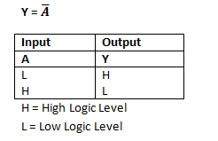
Schmitt Trigger gate is a digital logic gate, designed for arithmetic and logical operations. It provides OUTPUT based on INPUT voltage level. A Schmitt Trigger has a THERSHOLD voltage level, when the INPUT signal applied to the gate has a voltage level higher than the THRESHOLD of the logic gate, OUTPUT goes HIGH. If the INPUT signal level is lower than THRESHOLD, the OUTPUT of gate will be LOW.
In the chosen chip the Schmitt Trigger gate is followed by a NOT gate, So we get logic OUTPUT opposite to Schmitt Trigger OUTPUT. So the OUTPUT of INVERTED Schmitt Trigger will be LOW when the INPUT signal voltage level crosses THRESHOLD level of gate, in all other cases the OUTPUT will be HIGH.
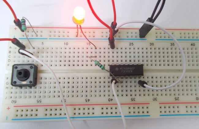
Here we are going to use 74LS14 IC for demonstration, this chip has 6 Schmitt Trigger gates in it. These SIX gate are connected internally as shown in below figure.
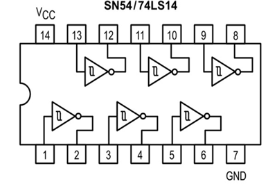
These gates have limitations for working voltage and input logic frequency. When these limitations are not considered the chip may damage permanently, so one should pay attention while selecting the logic gates.
Components
Power supply (5v)
1K, 220Ω resistors
74LS14 HEX SCHMITT TRIGGER GATE IC
1 LED, button
100nF capacitor
Connecting wires and breadboard
Circuit Diagram & Explanation
The truth table of Inverted Schmitt Trigger gate is shown in below figure.
As of circuit diagram an Inverted Schmitt Trigger gate has one output for one input. As by the truth table, the output of NOT gate will be high when the input is low. The output of NOT gate should be low when the input is high.
So the NOT gate provides output which is inverted logic of input, except the INPUT signal voltage level must cross THREHOLD voltage of Schmitt Trigger gate. If not the NOT gate followed by Schmitt Trigger will not see any INPUT and so the OUTPUT will be HIGH all the time.
In this circuit we are going to pull down both input of a gate to ground through a 1KΩ resistor. And then the input is connected to power through a button.
So when the button is pressed the corresponding pin of gate goes high. So with this button we can realize the truth table of Inverted Schmitt Trigger gate. When the button is pressed the input will go high, with this the output will go low and so the LED should be off. When the button is released the input will go LOW, with this the OUTPUT will go HIGH and so the LED should be ON.

These pull down resistor are necessary as the chosen CHIP is a positive edge triggering one. If the resistor is ignored the circuit might generate unpredictable results.
The capacitor here is for neutralizing the bouncing effect of button. Although the capacitor here is not compulsory, putting them might smooth the working of gate. The main purposes of Schmitt Trigger gate is for nullifying the bouncing effect of the buttons.
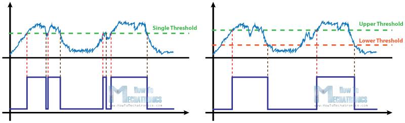
The Schmitt Trigger is a logic input type that provides hysteresis or two different threshold voltage levels for rising and falling edge. This is useful because it can avoid the errors when we have noisy input signals from which we want to get square wave signals.

So for example, if we have a noisy input signal like this, that is meant to have 2 pulses, a device that has only one set point, or threshold, could get incorrect input and it could register more than two pulses as shown in this illustration. And if we use the Schmitt Trigger for the same input signal we will get a correct input of two pulses because of the two different thresholds. So that’s the primal function of the Schmitt Trigger, to convert noisy square waves, sine waves or slow edges inputs into clean square waves.
Types of Schmitt Trigers
There are many logic ICs that have built-in Schmitt Triggers on their inputs, but also it can be built using transistors or easier using an Operational Amplifier, or comparator and just adding some resistors to it and a positive feedback.
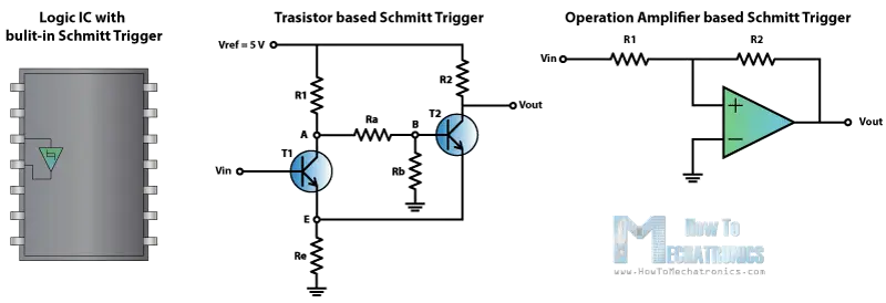
Operational Amplifier based Schmitt Trigger
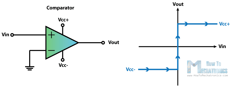
Here we have an op-amp which inverting input is connected to the ground or zero volts and the non-inverting input is connected to a voltage input, VIN. So this is actually a comparator and compares the non-inverting input to the inverting input or in this case the input voltage VIN to 0 V. So when the VIN value is below 0 volts the output of the comparator will be the negative VCC and if the input voltage is above 0 volts the output will be positive VCC.
Now if we add a positive feedback by connecting the output voltage to the non-inverting input with a resistor between them and another resistor between the VIN and the non-inverting input we will get the Schmitt Trigger. Now the output will switch from VCC– to VCC+ when the voltage at the A node will cross 0 volts.
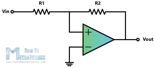
That means that now by adjusting the values of the resistors we can set at what value of the VIN input the switch will occur using the following equations. We get these equations with the following relationships. The current “i” through this line equals VIN – VA divided by R1 as well as VA – VOUT divided by R2. So if we replace the VA with zero, as we need that value for the switch to occur, we will get that final equation. For example if the output is -12 volts and the VIN input is negative and rises, the switch from -12 V to +12 V will occur at 6 volts according to the equation and the values of the resistors and vice versa when the VIN input is high and declines the switch from +12 V to – 12V will occur at -6 volts.
Non-Symmetrical Schmitt Trigger
In order to get two different non-symmetrical thresholds, we can use this circuit of an inverting single powered Schmitt Trigger. Here the VREF voltage is the same as the VCC of the op-amp. Now because the VIN input is connected to the inverting input of the op-amp when its values will reach the upper threshold, the output will switch off to 0 volts, and then when its values will decline to the lower threshold, the output will switch on to 5 volts.
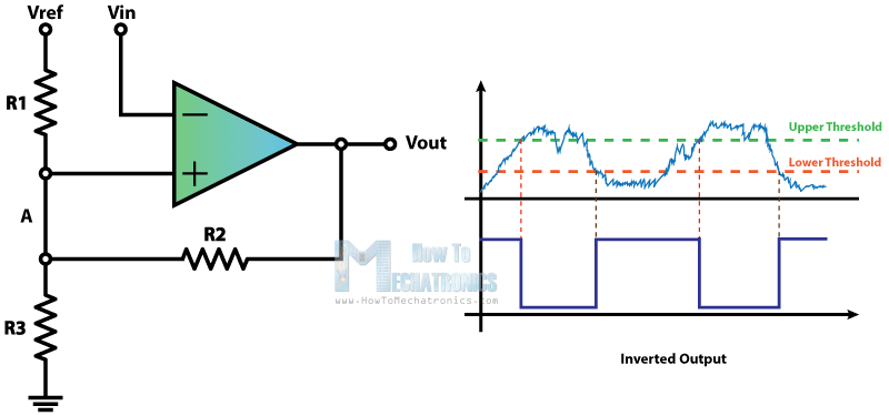
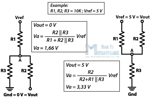
Here’s an example of how we can calculate the thresholds. The VREF and the VCC will be 5 volts and the three resistors will be the same 10k ohms. So what we need to calculate now is the voltage at the A node. In the first case when the output is 0 V our circuit will look like this, a simple voltage divider and the value of the VA will be 1.66 V. This means that the VIN input needs to decline below that value in order the output to switch on to 5 volts. Now with this 5 volts at the output the circuit will look like this. The value of the VA will be 3.33 V. This means that the VIN input needs to rise above that value in order the output to switch off to 0 volts.

Multivibrators and their Types

s circuits got more and more complicated over the years, it became impossible to have advanced applications without multiple states. Just think about it. What if a certain device of yours had only one state and no settings? This was the sort of problem faced earlier, when circuits were growing in complexity, and required components that could facilitate more efficient operation with multiple outputs. In modern terms, what if your microwave oven could only heat for say 30 seconds, nothing more, nothing less? They’re not directly related of course, but it’s just something we’re used to, electronic devices with multiple functions and outputs, multiple states, so to speak. So a multivibrator can be defined as an electronic circuit that is used to implement two state systems like oscillators, timers and flip-flops. Here’s all you need to know about them and their types!
History of Multivibrators
Back in 1919, Henri Abraham and Eugene Bloch described the first multivibrator circuit, also called a plate-coupled multivibrator. Made from vacuum tubes and introduced in 1920, it was christened the ‘Abraham-Bloch multivibrator oscillator’. It was simple yet progressive, and used harmonics to calibrate a wavemeter in the center. The whole setup was rather large because of the use of vacuum tubes, and gave way to more popular circuits. In fact, the Eccles-Jordan trigger is often said to be the original multivibrator circuit, when in reality, it was derived from the Abraham-Bloch multivibrator oscillator. It is, however, considered to be the first electronic flip-flop, and is named after William Eccles and F.W. Jordan.

The Eccles-Jordan trigger also made use of vacuum tubes, and was used in early computers, even in transistorized form. Basically, the fundamental flip-flop circuit introduced here was in use for a long time after, hence the popularity. Flip-flop types as we know them, were first described in 1954 by Montgomery Phister, in a course on computer design at the University of California, Los Angeles (UCLA). The Eccles-Jordan trigger was the first bistable multivibrator, a type that we will describe below. Over the years, the terminologies for multivibrators and flip-flops became more defined, and the terms as we know it were formed. Earlier, even monostable multivbrators were sometimes called flip-flops, which we now use only to refer to bistable multivibrators.

Types of Multivibrators
The name ‘multivibrator‘, originally came from the original oscillator version of the circuit, because of the harmonics seen in the output waveform. It became the generalized term for the circuit, and over the years more specific types of the circuit arose, which are:
Astable Multivibrator
A multivibrator circuit in which there is no single stable state is known as an astable multivibrator, as the name suggests. Basically the circuit keeps switching from one state to another, and while that theoretically sounds undesirable, there are actually many practical applications for it, namely, relaxation oscillators. It consists of two amplifying stages connected by coupling networks, with a positive feedback loop. The actual amplifying elements used range from vacuum tubes to op-amps and many more, including field effect transistors and bipolar junction transistors.

The circuit keeps switching from one state to another because of the positive feedback, and has only one amplifying element running at a time. The charge cycle is much faster compared to the discharge cycle, and is facilitated by the coupling capacitors, since voltage change in a capacitor cannot be instantaneous. Just like other circuits, it requires some time to begin conducting, which depends on the amplifying elements used.
Applications
- Used in applications where low clock frequency clock pulse train is required
- Relaxation oscillators, which are parts of vehicle indicator lights, disco strobe lights, early oscilloscopes and television receivers
- Timing signals
Monostable Multivibrator
A monostable multivibrator, as the name suggests, is a circuit with a single stable state. Conceptually and practically, it can be termed as a half astable multivibrator. While an astable multivibrator uses two resistive-capacitive networks, a monostable multivibrator uses one resistive-capacitive and one simple resistive network, hence it being called a half astable multivibrator. It outputs a perfect square waveform because of the absence of a loaded capacitor, and is used in precise applications.

The circuit, when triggered by an input pulse, switches to the unstable state for some time, then returns to the stable state. Depending on the application, the circuit can be tweaked to stay in the unstable state for as long as required, even sometimes requiring multiple input pulses to keep it in the unstable state. This is also called a retriggerable monostable multivibrator. Consequently, if the trigger pulses don’t affect the time spent in the unstable state, it is called a non-retriggerable monostable multivibrator.
Applications:
- Used as pulse generators
- Used to produce time delay in circuits
- Used to regenerate pulses in old telecommunication systems
- Used to reduce pulse distortion in computer systems
- Used as gated circuits
Bistable Multivibrator
A bistable multivibrator is a circuit that has two stable states. Instead of using two resistive-capacitive networks like an astable multivibrator, a bistable multivibrator uses two resistive networks only. Therefore it uses only direct or resistive coupling, and the latch type has no charge or discharge time because of the lack of any capacitors. Switching between the states can be done by two terminals called set and reset. Bistable multivibrators are among the most important components of digital computer systems, because they’re used to store data. It is also the basic storage element in sequential logic, and can be clocked or unclocked. Just like other types of multivibrators, bistable multivibrators also use multiple control elements, such as vacuum tubes and bipolar junction transistors. In complex circuits, multiple bistable multivibrators are cascaded as well.

As flip-flops, it can be divided into a few common types:
- Set-Reset Latch: An electronic device that requires no control input, and depends entirely on the state of the S and R signals. It is a simple circuit made from both NOR and NAND gates. As in, there are SR NOR latches, as well as SR NAND latches.
- Gated Latches: Similar to set-reset latches, these electronic devices often have an extra pair of NAND/NOR gates. So it requires an extra input before the set-rest inputs can be activated. This extra input is also termed as the ‘Enable’ input, since it enables the usage of the set and reset inputs.
- D Flip-Flop: Also known as the ‘Data’ or ‘Delay’ flip-flop, this widely used electronic device finds application in memory, delay lines or a zero cell hold. Practically, it’s the basis for shift registers, a highly important part of many electronic devices. It basically holds the current value of D input.
- T Flip-Flop: T Flip-Flops are also known as toggle flip flops, and change their output on each clock edge, which is usually half the frequency of the signal to the T input. They are used extensively in frequency dividers, binary counters and binary addition devices.
- JK Flip-Flop: Known as the universal flip-flop, JK flip-flops are similar to SR NAND latches, except that there is no forbidden input, even when both set and reset are 1. It is basically a gated SR flip-flop with an additional input clock circuit for extra stability. There are four possible outputs in this case, namely logic 1, logic 0, toggle and no change.
Bistable multivibrators, particularly flip-flops, are subject to something called metastability, which happens when both inputs change at the same time. It can cause unforeseen problems like extra time to settle into a state, unintended oscillations and the like. In digital computer systems, this can lead to data corruption and crashes because of the inconsistent state change. This is fixed by setting proper time constraints and cascading multiple flip-flops.
Applications:
- Used in counting circuits
- Used in memory storage units
- Used as frequency dividers
- Used in pulse generation circuits

Phosphatase sharing facilitates transition from the monostable to bistable response (phenotype). (A) The time course of the median fitness of bistable or monostable phenotype over 1000 simulation trajectories with different starting genotypes (parameter values). The top panel shows the median evolutionary trajectories for transition from monostable to bistable and the bottom panel shows the same for the bistable to monostable transition. (B) shows corresponding distributions of the fitness for monostable to bistable transitions with the generation time for the three cases. The results reveal that the transition/adaptation speed toward bistability is a function of degree of phosphatase sharing, with fully shared > partially shared > unshared. The transition speeds are comparable for bistability to monostability transition (bottom panel in A). (C) The median evolutionary trajectories with a starting mixture of the three cascades, each with a population size of 100, evolving toward bistability (left panel) or monostability (right panel) for 100 different genotypes, indicate that the fully shared cascade quickly outcompetes the other two topologies as it transitions to bistability.
Conclusion
Thus, multivibrators are very important electronic devices, used in a wide range of applications. As seen above, they’re more of the basic building blocks of electronics and computer systems, and began from simpler vacuum tubes. While earlier they found use in television sets, frequency dividers and the like for synchronizing purposes, evolved versions of them are now used in complex computer systems and form the very basic forms of memory. On the other hand, they’re also used in simple turn signal circuits seen in vehicles around the world, which is testament to their versatility. Our basic notion of multiple operation, types and states stems from these devices, without which we’d probably be stuck with much simpler devices. It’s quite interesting to see how multivibrators give way to devices like oscillators and flip-flops, which in turn turn into something more complex, so on and so forth.
A. XO One SHOT NOR Gate Monostable
_____________________________________________________________________

Suppose initially that the trigger input is LOW at a logic level “0” so that the output from the firstNOR gate U1 is HIGH at logic level “1”, (NOR gate principals). The resistor, RT is connected to the supply voltage so is also equal to logic level “1”, which means that the capacitor, CT has the same charge on both of its plates. Junction V1 is therefore equal to this voltage so the output from the second NOR gate U2 will be LOW at logic level “0”. This then represents the circuits “Stable State” with zero output.
When a positive trigger pulse is applied to the input at time t0, the output of the first NOR gate U1goes LOW taking with it the left hand plate of capacitor CT thereby discharging the capacitor. As both plates of the capacitor are now at logic level “0”, so too is the input to the second NOR gate, U2resulting in an output equal to logic level “1”. This then represents the circuits second state, the “Unstable State” with an output voltage equal to +Vcc.
The second NOR gate, U2 will maintain this second unstable state until the timing capacitor now charging up through resistor, RT reaches the minimum input threshold voltage of U2 (approx. 2.0V) causing it to change state as a logic level “1” value has now appeared on its inputs. This causes the output to be reset to logic “0” which in turn is fed back (feedback loop) to one input of U2. This action automatically returns the monostable back to its original stable state and awaiting a second trigger pulse to restart the timing process once again.

Square and Pulse Generator Block Diagram are used as measuring devices in combination with a CRO. They provide both quantitative and qualitative information of the system under test. They are made use of in transient response testing of amplifiers. The fundamental difference between a pulse generator and a square wave generator is in the duty cycle.

A square wave generator has a 50% duty cycle. 8.9.1
Requirements of a Pulse
- The pulse should have minimum distortion, so that any distortion, in the display is solely due to the circuit under test.
- The basic characteristics of the pulse are rise time, overshoot, ringing, sag, and undershoot.
- The pulse should have sufficient maximum amplitude, if appreciable output power is required by the test circuit, e.g. for magnetic core At the same time, the attenuation range should be adequate to produce small amplitude pulses to prevent over driving of some test circuit.
- The range of frequency control of the pulse repetition rate (PRR) should meet the needs of the experiment. For example, a repetition frequency of 100 MHz is required for testing fast circuits. Other generators have a pulse-burst feature which allows a train of pulses rather than a continuous
- Some pulse generators can be triggered by an externally applied trigger signal; conversely, pulse generators can be used to produce trigger signals, when this output is passed through a differentiator circuit.
- The output impedance of the pulse generator is another important In a fast pulse system, the generator should be matched to the cable and the cable to the test circuit. A mismatch would cause energy to be reflected back to the generator by the test circuit, and this may be re-reflected by the generator, causing distortion of the pulses.
- DC coupling of the output circuit is needed, when dc bias level is to be
The basic circuit for pulse generation is the asymmetrical multi-vibrator. A laboratory type square wave and pulse generator is shown in Fig. 8.6.
The frequency range of the instrument is covered in seven decade steps from 1 Hz to 10 MHz, with a linearily calibrated dial for continuous adjustment on all ranges.

The duty cycle can be varied from 25 – 75%. Two independent outputs are available, a 50 Q source that supplies pulses with a rise and fall time of 5 ns at 5 V peak amplitude and a 600 Q source which supplies pulses with a rise and fall time of 70 ns at 30 V peak amplitude. The instrument can be operated as a free-running generator, or it can be synchronised with external signals.
The basic generating loop consists of the current sources, the ramp capacitor, the Schmitt trigger and the current switching circuit, as shown in Fig. 8.7.

The upper current source supplies a constant current to the capacitor and the capacitor voltage increases linearly. When the positive slope of the ramp voltage reaches the upper limit set by the internal circuit components, the Schmitt trigger changes state. The trigger circuit output becomes negative and reverses the condition of the current switch. The capacitor discharges linearly, controlled by the lower current source. When the negative ramp reaches a predetermined lower level, the Schmitt trigger switches back to its original state. The entire process is then repeated. The ratio i1/i2 determines the duty cycle, and is controlled by symmetry control. The sum of i1 and i2 determines the frequency. The size of the capacitor is selected by the multiplier switch.
The unit is powered by an internal supply that provides regulated voltages for all stages of the instrument.

+++++++++++++++++++++++++++++++++++++++++++++++++++++++++++++++++++++++
e- Trigger On kinds of trigger electronic circuits to be junction electronic component for trigger


++++++++++++++++++++++++++++++++++++++++++++++++++++++++++++++++++++++++
Tidak ada komentar:
Posting Komentar