

when communication data and data storage and its accumulation on communication computer networks that exist on earth at this time can use cloud intermediary media as a catalyst for computer network communication which is expected at one time and time when computer networks and electronic communications on earth have independent energy consumption Efficient outside of the initial start-up use of electric media generators and adapters to turn on and turn off computer networks, which is certainly when we can use energy above the clouds to turn on independent energy for the equipment of computer communication networks and also possible star energy in the sky for energy storage continued, which of course we can excavate using future electronic engineering techniques, namely at proxy wells on earth as well as fire wall wells that surround computer network systems on earth before entering into the computer network diagnostic window system. on earth .
Love ( Line On Victory Endless )

Gen. Mac Tech Zone cloud energy and above the cloud
energy-efficient is cloud computing
Researchers have found that, at high usage levels, the energy required to transport data in cloud computing can be larger than the amount of energy required to store the data.
Conventionally, data storage and data processing are done at the user's own computer, using that computer's storage system and processor. An alternative to this method is cloud computing, which is Internet-based computing that enables users at home or office computers to transfer data to a remote data center for storage and processing. Cloud computing offers potential benefits – especially financial ones – to users, but in a new study, researchers have investigated a different aspect of cloud computing: how does its energy consumption compare with conventional computing?
cloud computing is not always the greenest option. They investigated using cloud computing for three different services – storage, software, and processing – on public and private systems. (A public cloud is hosted on the Internet, and a private cloud is hosted within a company behind its firewall.) While previous studies of energy consumption in cloud computing have focused only on the energy consumed in the data center, the researchers found that transporting data between data centers and home computers can consume even larger amounts of energy than storing it.
“The most important conclusion in our analysis is that, when comparing the energy consumption of cloud-based services with that of a typical desktop PC, we must include the energy consumption required to transport the data from the user into the cloud resources and back,” Rod Tucker, leader of the University of Melbourne research team, told PhysOrg.com. “This is particularly important if the cloud service is provided via the public Internet. Some papers that have claimed that cloud computing provides a 'greener' alternative to current desktop computing fail to include the energy consumption involved with transporting the data from the user into the cloud. In many cases, we may find that the data center used by the cloud-based services are located in another city, state or even country.”
In general, not much attention has been paid to the energy consumption used in transmitting data, since cloud computing is more often praised for its other features. Some advantages of cloud computing are that it offers high-capacity storage and high-performance computing from any location with Internet access, while not requiring users to invest in new hardware or upgrade their software. Cloud computing systems can be free (such as Google Docs), or users may pay a yearly subscription fee or fee per resources used.
“Energy efficiency is crucial in two contexts,” Tucker said. “Firstly, if the user device is a mobile device (phone, i-pad, PDA, etc.), then its battery lifetime is a key issue. Secondly, as the use of cloud services balloons, its energy consumption will likewise grow. The US Environmental Protection Agency estimated that in 2007 servers and data centers were responsible for about 0.5% of US greenhouse gas production. The greenhouse gas production that results from power consumption of data centers is expected to double between 2007 and 2020 if we just continue with business as usual. Without careful consideration of the power consumption of cloud services, their growing popularity will become a significant contributor to greenhouse gas production. Therefore, we need to develop technologies and strategies to address this issue before cloud services become more widespread.”
When using the cloud for data storage (such as storing documents, photos, and videos using services such as Amazon Simple Storage), the researchers found that cloud computing can consume less power than conventional computing when the cloud service is used infrequently and at low intensities. This is because, at low usage levels, power consumption for storage dominates total power consumption, and power consumption for transport is minimal. But at medium and high usage levels, more energy is required to transport data, so that transport dominates total power consumption and greatly increases the overall energy consumed. Specifically, power for transport can be as low as 10% and 25% at low usage levels for private and public storage services, respectively, and nearly 60% and 90%, respectively, at high usage levels.
But overall, cloud storage services use less energy compared to cloud software and cloud processing. For cloud software services (such as Google Docs), the power consumption in transport is negligibly small as long as screen refresh rates are low (lower than 0.1 frames/sec, where 1 frame/sec means that 100% of the screen changes every second; a smaller percentage of the screen changing corresponds to a smaller screen refresh rate). However, for cloud software services, the biggest factor determining energy efficiency is the number of users per server, where more users corresponds to lower power consumption per user. In this case, public cloud computing, with its larger number of users, would benefit more than private cloud computing.
For cloud processing services (in which a server such as Amazon Elastic Compute Cloud processes large computational tasks only, and smaller tasks are processed on the user's computer), the researchers again found that the cloud alternative can use lower consumption only under certain conditions. The results showed that, for public cloud processing services, data transport consumed large amounts of energy compared to private cloud processing services, particularly at high usage levels. The reason is that the large number of router hops required on the public Internet greatly increases the energy consumption in transport, and private cloud processing requires significantly fewer routers. Still, the researchers found that, for both public and private clouds, a cloud processing service is more energy-efficient than older-generation PCs.
The results of the study mean different things for different users. As the researchers explain, home computer users can achieve significant energy savings by using low-end laptops for routine tasks and cloud processing services for computationally intensive tasks that are infrequent, instead of using a mid- or high-end PC. For corporations, it is less clear whether the energy consumption saved in transport with a private cloud compared to a public cloud offsets the private cloud's higher energy consumption. Private clouds that serve a relatively small number of users may not benefit from the same energy-saving techniques due to their smaller scale.
Overall, the researchers predict that the technology used in cloud computing – for example, data centers, routers, switches, etc. – will continue to become more energy-efficient. Most importantly, they recommend that one of the biggest areas of improvement is improving the energy efficiency of data transport, especially as cloud computing becomes more widespread.
“Many industry participants see the evolution toward mobility will intrinsically mean an evolution toward cloud-based services,” Tucker said. “The reason is that mobile access devices will have limited processing and storage capacity (due to size and power constraints) and so the most convenient place to put the applications and data is in the cloud. The user device will contain little more than a browser when it is started up. Any application or data that it requires will be brought down from the cloud. When that application is finished, its data will be put back into the cloud and the application will be removed from the user device until it is again required. In this way, the user device is kept simple, energy-efficient and cheap.”
Cloud computing gathers steam with mobile devices
The outlook for the wireless industry is getting cloudier. Consumers have tapped into cloud computing technology for years: sending messages via Hotmail, uploading photos to Facebook or editing a spreadsheet on Google Docs are just a few examples. Simply put, cloud computing moves data from a single machine, such as a personal computer, to the Internet. The technology frees users from needing to be at a specific PC to access saved information.
Now the cloud is going mobile, and industry players expect the number of mobile cloud computing applications and Web-enabled portable devices to grow rapidly over the next few years. Motorola is building much of its turnaround strategy for mobile phones on a cloud-based solution, and wireless broadband service provider Clearwire believes the advent of faster, more sophisticated networks will unleash the full power of cloud computing.
If the industry projections come true, cloud computing will be even more commonplace. Colleagues may edit the same document over the Internet, with one person on a home computer and the other using a touch screen built into the back of the driver's seat of a car. Or a tourist who takes photos on a phone could store them in an online album, then view the pictures from a laptop.
AT&T has seen its network burdened by the large amount of data being consumed by iPhone users, and the strain across wireless networks will increase with growth in mobile applications and user-generated content.
"The biggest component (of mobile cloud computing) is you have to have a fat pipe wherever you are
faster networks will dovetail with the proliferation of smarter devices. "This is going to be much more accessible to a lot of us on affordable phones,
XO__XO WHAT IS A DATA CENTER? Tomorrow and Future
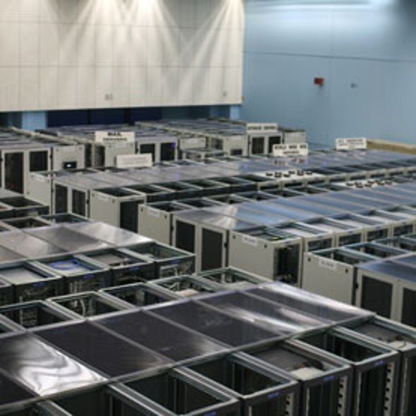
A data center is a facility that centralizes an organization’s IT operations and equipment, as well as where it stores, manages, and disseminates its data. Data centers house a network’s most critical systems and are vital to the continuity of daily operations. Consequentially, the security and reliability of data centers and their information is a top priority for organizations.
Although data center designs are unique, they can generally be classified as internet-facing or enterprise (or “internal”) data centers. Internet-facing data centers usually support relatively few applications, are typically browser-based, and have many users, typically unknown. In contrast, enterprise data centers service fewer users, but host more applications that vary from off-the-shelf to custom applications.
Data center architectures and requirements can differ significantly. For example, a data center built for a cloud service provider like Amazon® EC2 satisfies facility, infrastructure, and security requirements that significantly differ from a completely private data center, such as one built for the Pentagon that is dedicated to securing classified data.
Regardless of classification, an effective data center operation is achieved through a balanced investment in the facility and equipment housed. The elements of a data center break down as follows:
Facility – the location and “white space,” or usable space, that is available for IT equipment. Providing round-the-clock access to information makes data centers some of the most energy-consuming facilities in the world. A high emphasis is placed on design to optimize white space and environmental control to keep equipment within manufacturer-specified temperature/humidity range.
Support infrastructure – equipment contributing to securely sustaining the highest level of availability possible. The Uptime Institute defined four tiers data centers can fall under, with availability ranging from 99.671% to 99.995%. Some components for supporting infrastructure include:
- Uninterruptible Power Sources (UPS) – battery banks, generators and redundant power sources.
- Environmental Control – computer room air conditioners (CRAC), heating, ventilation, and air conditioning (HVAC) systems, and exhaust systems.
- Physical Security Systems – biometrics and video surveillance systems.
IT equipment – actual equipment for IT operations and storage of the organization’s data. This includes servers, storage hardware, cables and racks, as well as a variety of information security elements, such as firewalls.
Operations staff – to monitor operations and maintain IT and infrastructural equipment around the clock.
Data centers have evolved significantly in recent years, adopting technologies such as virtualization to optimize resource utilization and increase IT flexibility. As enterprise IT needs continue to evolve toward on-demand services, many organizations are moving toward cloud-based services and infrastructure. A focus has also been placed on initiatives to reduce the enormous energy consumption of data centers by incorporating more efficient technologies and practices in data center management. Data centers built to these standards have been coined “green data centers.”
To address growing data center demands and provide the added benefits of agility, scalability and global reach, the traditional data center is transforming into what is commonly referred to as a hybrid data center.
A hybrid cloud combines your existing data center (private cloud) resources, over which you have complete control, with ready-made IT infrastructure resources (e.g., compute, networking, storage, applications and services) that provide bursting and scaling capabilities found in IaaS (infrastructure as a service) or public cloud offerings, such as Amazon® Web Services (AWS®).
Here are three key benefits of using a hybrid cloud approach:
Benefit 1: Start Small and Expand as Needed
A hybrid cloud approach enables you to license IT infrastructure resources on a project-by-project basis with the ability to add more as needed. Without the public cloud, you would potentially invest in hardware that would sit idly during off-peak times and only be used for short-term projects.
A hybrid cloud also lets you take advantage of component-based development methodologies. If you use AWS for building new applications, architects and coders can leverage development techniques that are more component-based than previously used techniques. You can easily separate development, testing and production environments for new applications. Environments can be cloned or replicated, spooled up, and used as needed with seamless traffic flow and strong security policy enforcement.
Benefit 2: Expand Your Data Center Seamlessly and Transparently
With a hybrid strategy, your public cloud essentially functions as an extension of your data center via an IPsec VPN connection, allowing you to safely and securely deploy workloads in either location. The IPsec VPN connection acts as an overlay network, bringing added benefits of privacy and simplicity from the reduction in the number of Layer 3 hops across the end-to-end network. This allows you to transparently expand your internal IP address space into the public cloud using widely supported routing protocols. With an overlay network, there’s nothing new or challenging to your network operations team or security specialists, and security policies can be easily extended to cover the routes.
Benefit 3: Security Policy Consistency – From the Network to the Cloud
Your business relies on the consistent, reliable operation of applications and data whether on-premise or in the cloud. To ensure your applications and data are protected from cyber adversaries, best practices dictate that your policies be consistent and, ideally, managed centrally. By centrally managing your on-premise and public cloud security policies, you are able to perform logical groupings of like rules, security objects and so on. This creates many opportunities for improved efficiency using a single pane of glass for all your firewalls, public and private.
For example, many configuration elements universal to all firewalls in your organization can be configured once and shared with all firewalls, including such elements as DNS servers, NTP servers, local admin accounts and syslog servers.
Secure the Hybrid Cloud With VM-Series
The hybrid cloud offers significant benefits for organizations: You can start small, expand as needed, and extend your data center into the public cloud securely with the same security policy constructs in use in your private cloud. Palo Alto Networks® VM-Series virtualized next-generation firewall enables you to securely deploy a hybrid cloud by protecting your applications and data in AWS.
Cloud Computing Saves Energy
consolidating pictures, videos, e-mails and documents on remote servers saves more energy than keeping them on personal computers
When it comes to computing, the "cloud" may rain efficiency benefits.
Researchers at Lawrence Berkeley National Laboratory and Northwestern University unveiled a modeling tool yesterday that estimates the energy savings of moving local network software and computing into the server farms that make up the cloud.
The tool, available to the public online, is called the Cloud Energy and Emissions Research Model (CLEER). It aims to give scientists a better understanding of how energy use changes as the world moves away from storing and processing information in local networks and moves toward outsourcing these tasks to centralized facilities.
Though the word "cloud" evokes images of a clean, simple and environmentally friendly process, the systems that support it are massive industrial facilities, densely packed with processors and hard drives, that devour energy by the megawatt. Data centers use between 1 and 2 percent of the world's electricity and, with dead trees that make paper giving way to magnetic disks, energy use and consequently emissions from the Internet is poised to surge further
Nonetheless, moving to the cloud could still save huge amounts of energy.
In a case study using the CLEER simulation, researchers found that if all American businesses moved their email programs, spreadsheet applications, customer management software and the like to centralized off-site servers, companies would shrink their computing energy footprints by 87 percent, enough to satiate the 23 billion kilowatt-hour annual appetite for the city of Los Angeles.
"The main gains in cloud computing come from consolidation," a scientist at Berkeley Lab who co-authored the study. Many businesses have servers and computing hardware on-site, which are often inefficient and underused, soaking up electricity while sitting idle.
Pooling these resources in a central location means companies can effectively buy computing power in bulk and servers can spend more time doing actual work per processing unit, reducing the overall need for more computers.
A counterintuitive finding
It seems to make intuitive sense, but researchers said they had some difficulty confirming their suspicions that the cloud saves energy. "There is a gap here where there is not enough data," Ramakrishnan said.
It seems to make intuitive sense, but researchers said they had some difficulty confirming their suspicions that the cloud saves energy. "There is a gap here where there is not enough data," Ramakrishnan said.
Another issue is that there are so many variables at play. "The savings are really going to vary depending on the system you're studying and what your baseline
Whether watching a video uses less energy when it is streamed compared to a DVD depends on your computer, how you use it, the quality of your Internet connection and server loads, along with a host of other factors.
"The analyses that we need for understanding the net implications of these new technologies can be quite complex,
"There are a lot of moving parts that determine whether it's a good or bad thing."
The CLEER Model starts to chip away at this problem, aggregating available models of how data moves through the Internet. It then calculates the energy used to deliver the ones and zeros as well as the carbon intensity behind it, since not all electrons are created equal; electricity from dirty fuels like coal or from renewable sources, like solar and wind power, changes the overall environmental impact from the cloud.
There are also some limitations to CLEER. "We didn't include things like cost and latency and other things that come into play when you're making a business decision," Masanet said. However, researchers can rebuild and reconfigure the model from the bottom up as better data come in.
Eventually, Internet companies could tell you just how efficient their data centers are using tools like CLEER, increasing energy transparency and letting consumers shop for the most efficient option.
A new wireless technology on computer science and engineering.
“it transforms existing wireless signals into both a source of power and a communication medium. It enables two battery-free devices to communicate by backscattering existing wireless signals. Backscatter communication is orders of magnitude more power-efficient than traditional radio communication. Further, since it leverages the ambient RF signals that are already around us, it does not require a dedicated power infrastructure as in RFID.”
“It’s hopefully going to have applications in a number of areas including wearable computing, smart homes and self-sustaining sensor networks,”
“We can reflect these signals slightly to create a Morse code of communication between battery-free devices.”
The researchers tested the ambient backscatter technique with credit card-sized prototype devices placed within several feet of each other. Groups of the devices were tested in a variety of settings in the Seattle area, including inside an apartment building, on a street corner and on the top level of a parking garage. These locations ranged from less than half a mile away from a TV tower to about 6.5 miles away.
They found that the devices were able to communicate with each other, even the ones farthest from a TV tower. The receiving devices picked up a signal from their transmitting counterparts at a rate of 1 kilobit per second when up to 2.5 feet apart outdoors and 1.5 feet apart indoors. This is enough to send information such as a sensor reading, text messages and contact information. It’s also feasible to build this technology into devices that do rely on batteries, such as smartphones. It could be configured so that when the battery dies, the phone could still send text messages by leveraging power from an ambient TV signal.
The researchers are not the only people looking at solving the problem of mobile / wireless power. The Wireless Power Consortium have created a standard called Qi (pronounced "Chee") which uses inductive electrical power transfer over distances of up to 4 cm (2 inches). The Qi system comprises a power transmission pad and a compatible receiver in a portable device. To use the system, the mobile device is placed on top of the power transmission pad, which charges it via electromagnetic induction .
The researchers are not the only people looking at solving the problem of mobile / wireless power. The Wireless Power Consortium have created a standard called Qi (pronounced "Chee") which uses inductive electrical power transfer over distances of up to 4 cm (2 inches). The Qi system comprises a power transmission pad and a compatible receiver in a portable device. To use the system, the mobile device is placed on top of the power transmission pad, which charges it via electromagnetic induction. But unlike the UW researcher’s technology, the Qi specification is primarily targeting the recharging of a device rather than the actual powering of it.
The applications of true long haul wireless power transmission are as broad as they are exciting as Time .
“given their size and wireless self-sufficiency, imagine these sensors embedded in everything from structures to vehicles to clothing. An office in a skyscraper might alert someone that a window’s been left open; a vehicle might alert you if the child lock’s been tripped or that there’s change under the seat; running shoes could let you know when you’ve reached their optimal mileage threshold. Or consider : examples: bridges capable of alerting someone if stress-related cracks form, couches that sing out after they “eat” your keys and the option to send text messages or emails with “wearable” technology, battery-free.”
XO_XO ++ DW the earliest example of ADA ( Address - Data - Accumulation ) in the flash disk electronic circuit
Flash Drives Work :

You plug it in, grab an important file, and yank it out. It all seems so simple. But have you ever wondered what is going on inside your flash drive as your files are moving to and fro?
Perhaps you’re like most people: perfectly content to enjoy the usefulness of your flash drive without ever considering the mysterious flow of electrons between the myriad tiny components that make it up. And that’s okay. But sometimes, even for the blissfully ignorant, curiosity can be peeked when a device stops doing the thing it's supposed to do, like when a flash drive breaks or stops being recognized by your computer.
For the electronics lay person who wants a general idea of how flash drives work, the following info is for you.
Flash Drives vs. Hard Drives

A key difference between flash drives and other types of memory devices is the lack of moving parts. Flash drives are solid state, which means they store data on a piece of silicon with zillions of tiny transistors, as opposed to traditional hard drives which use magnetic spinning disks.
Each transistor on the silicon chip holds a single bit of binary digital information: either 1 or 0. In flash drives, the transistor is set to 1 by default. To change one of these transistors' states to 0, an electric charge resulting in a crazy little process called Fowler-Nordheim tunneling is required.
One cool thing about flash memory is that it doesn't require a power source to remember what is on it. In fact, if you bury your flash drive in your back yard and dig it up a thousand years from now, the data will still be on the memory chip just as you left it.
The Brain of a Flash Drive

Basically, the data on a memory chip is nothing more than a bunch of tiny ones and zeros. Making sense of those ones and zeros-telling them where to go and keeping track of where they are-is accomplished by the flash drive’s microcontroller. A flash drive’s microcontroller is roughly analogous to a computer’s CPU, or a human’s brain, but somewhat simpler, in most cases.
There is a vast array of brands and varieties of microcontrollers used by flash drive manufacturers. Some are better than others in terms of speed and durability. Second only to broken connectors, bad microcontrollers are the leading cause of flash drive failure.
How Flash Drives Communicate with Computers

USB flash drives talk with computers by means of either a standard USB 2.0 or USB 3.0 interface. At present, flash drives using the USB 3.0 interface are backwards compatible with the USB 2.0 plug.
USB 2.0 interfaces have four connections: a +5VDC power source, one positive and one negative data line, and a ground. USB 3.0 connectors have four additional data lines and a drain, creating a 10X increase in theoretical transfer speed.
In addition to the essential parts mentioned above, flash drive circuit boards are covered in lots of little surface mounted components like resistors, capacitors, diodes, oscillators, LEDs, and other parts, the primary purpose of which is to divide and direct electricity to the right places. we hope that helps unravel a little bit of the mystery behind the flash drive. Don’t forget to back up your flash drive and let us know if we can help you recover lost photos or other data. .
Flash Drives and The Cloud

Cloud storage platforms like Dropbox and Google Drive have some genuine advantages over USB flash drives: You obviously don't have to remember to bring your flash drive with you in order to access your files, and the risk of losing your files is relatively small compared to flash drives that can break, malfunction, be misplaced or get stolen. On the other hand, cloud storage also has its drawbacks. For many of us the issue of security is a deal breaker. Just today it would appear that Dropbox user accounts have once again been hacked. Even if you go in a change your password right away, in reality it may be too late. You won't know if hackers have accessed your private files until unknown charges appear on your bank statement, private pictures are posted online, etc.
One solution is to keep your sensitive files off of cloud storage and on a flash drive instead. If you tend to leave your flash drive at home, you might want to consider a flash drive that attaches to your key chain. Encrypting your flash drive with TrueCrypt or BitLocker adds an additional layer of security ( e- Key Shifting ) .


Flash memory
Imagine if your memory worked only while you were awake. Every morning when you got up, your mind would be completely blank! You'd have to relearn everything you ever knew before you could do anything. It sounds like a nightmare, but it's exactly the problem computers have. Ordinary computer chips "forget" everything (lose their entire contents) when the power is switched off. Large personal computers get around this by having powerful magnetic memories called hard drives, which can remember things whether the power is on or off. But smaller, more portable devices, such as digital cameras and MP3 players, need smaller and more portable memories. They use special chips called flash memories to store information permanently. Flash memories are clever—but rather complex too. How exactly do they work?
How computers store information
Computers are electronic machines that process information in digital format. Instead of understanding words and numbers, as people do, they change those words and numbers into strings of zeros and ones called binary (sometimes referred to as "binary code"). Inside a computer, a single letter "A" is stored as eight binary numbers: 01000001. In fact, all the basic characters on your keyboard (the letters A–Z in upper and lower case, the numbers 0–9, and the symbols) can be represented with different combinations of just eight binary numbers. A question mark (?) is stored as 00111111, a number 7 as 00110111, and a left bracket ([) as 01011011. Virtually all computers know how to represent information with this "code," because it's an agreed, worldwide standard. It's called ASCII (American Standard Code for Information Interchange).
Computers can represent information with patterns of zeros and ones, but how exactly is the information stored inside their memory chips? It helps to think of a slightly different example. Suppose you're standing some distance away, I want to send a message to you, and I have only eight flags with which to do it. I can set the flags up in a line and then send each letter of the message to you by raising and lowering a different pattern of flags. If we both understand the ASCII code, sending information is easy. If I raise a flag, you can assume I mean a number 1, and if I leave a flag down, you can assume I mean a number 0. So if I show you this pattern:
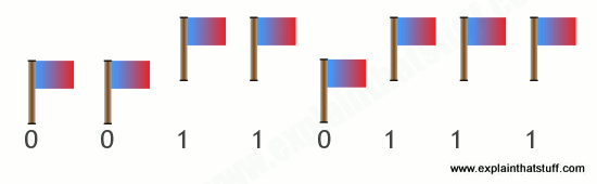
You can figure out that I am sending you the binary number 00110111, equivalent to the decimal number 55, and so signaling the character "7" in ASCII.
What does this have to do with memory? It shows that you can store, or represent, a character like "7" with something like a flag that can be in two places, either up or down. A computer memory is effectively a giant box of billions and billions of flags, each of which can be either up or down. They're not really flags, though—they are microscopic switches called transistors that can be either on or off. It takes eight switches to store a character like A, 7, or [. It takes one transistor to store each binary digit (which is called a bit). In most computers, eight of these bits are collectively called a byte. So when you hear people say a computer has so many megabytes of memory, it means it can store roughly that many million characters of information (mega means million; giga means thousand million or billion).
What is flash memory?
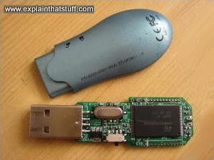
Photo: A typical USB memory stick—and the flash memory chip you'll find inside if you take it apart (the large black rectangle on the right).
Ordinary transistors are electronic switches turned on or off by electricity—and that's both their strength and their weakness. It's a strength, because it means a computer can store information simply by passing patterns of electricity through its memory circuits. But it's a weakness too, because as soon as the power is turned off, all the transistors revert to their original states—and the computer loses all the information it has stored. It's like a giant attack of electronic amnesia!
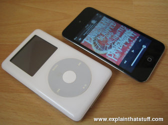
Photo: Apple iPods, past and present. The white one on the left is an old-style classic iPod with a 20GB hard drive memory. The newer black model on the right has a 32GB flash memory, which makes it lighter, thinner, more robust (less likely to die if you drop it), and less power hungry.
Memory that "forgets" when the power goes off is called Random Access Memory (RAM). There is another kind of memory called Read-Only Memory (ROM) that doesn't suffer from this problem. ROM chips are pre-stored with information when they are manufactured, so they don't "forget" what they know when the power is switched on and off. However, the information they store is there permanently: they can never be rewritten again. In practice, a computer uses a mixture of different kinds of memory for different purposes. The things it needs to remember all the time—like what to do when you first switch it on—are stored on ROM chips. When you're working on your computer and it needs temporary memory for processing things, it uses RAM chips; it doesn't matter that this information is lost later. Information you want a computer to remember indefinitely is stored on its hard drive. It takes longer to read and write information from a hard drive than from memory chips, so hard drives are not generally used as temporary memory. In gadgets like digital cameras and small MP3 players, flash memory is used instead of a hard drive. It has certain things in common with both RAM and ROM. Like ROM, it remembers information when the power is off; like RAM, it can be erased and rewritten over and over again.
How flash memory works—the simple explanation
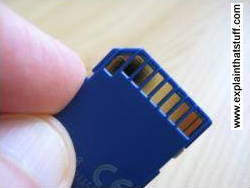
Photo: Turn a digital camera's flash memory card over and you can see the electrical contacts that let the camera connect to the memory chip inside the protective plastic case.
Flash works using an entirely different kind of transistor that stays switched on (or switched off) even when the power is turned off. A normal transistor has three connections (wires that control it) called the source, drain, and gate. Think of a transistor as a pipe through which electricity can flow as though it's water. One end of the pipe (where the water flows in) is called the source—think of that as a tap or faucet. The other end of the pipe is called the drain—where the water drains out and flows away. In between the source and drain, blocking the pipe, there's a gate. When the gate is closed, the pipe is shut off, no electricity can flow and the transistor is off. In this state, the transistor stores a zero. When the gate is opened, electricity flows, the transistor is on, and it stores a one. But when the power is turned off, the transistor switches off too. When you switch the power back on, the transistor is still off, and since you can't know whether it was on or off before the power was removed, you can see why we say it "forgets" any information it stores.
A flash transistor is different because it has a second gate above the first one. When the gate opens, some electricity leaks up the first gate and stays there, in between the first gate and the second one, recording a number one. Even if the power is turned off, the electricity is still there between the two gates. That's how the transistor stores its information whether the power is on or off. The information can be erased by making the "trapped electricity" drain back down again.
How flash memory works—a more complex explanation
That's a very glossed over, highly simplified explanation of something that's extremely complex. If you want more detail, it helps if you read our article about transistors first, especially the bit at the bottom about MOSFETs—and then read on.
The transistors in flash memory are like MOSFETs only they have two gates on top instead of one. This is what a flash transistor looks like inside. You can see it's an n-p-n sandwich with two gates on top, one called a control gate and one called a floating gate. The two gates are separated by oxide layers through which current cannot normally pass:
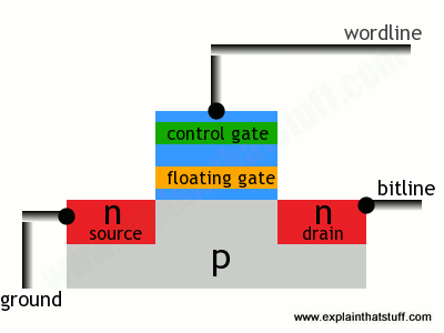
In this state, the transistor is switched off—and effectively storing a zero. How do we switch it on? Both the source and the drain regions are rich in electrons (because they're made of n-type silicon), but electrons cannot flow from source to drain because of the electron deficient, p-type material between them. But if we apply a positive voltage to the transistor's two contacts, called the bitline and the wordline, electrons get pulled in a rush from source to drain. A few also manage to wriggle through the oxide layer by a process called tunneling and get stuck on the floating gate:
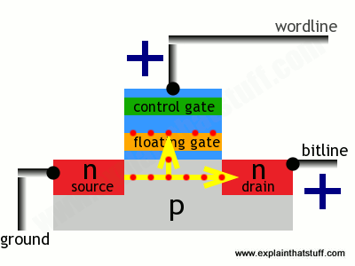
The presence of electrons on the floating gate is how a flash transistor stores a one. The electrons will stay there indefinitely, even when the positive voltages are removed and whether there is power supplied to the circuit or not. The electrons can be flushed out by putting a negative voltage on the wordline—which repels the electrons back the way they came, clearing the floating gate and making the transistor store a zero again.
Not an easy process to understand, but that's how flash memory works its magic!
How long does flash memory last?
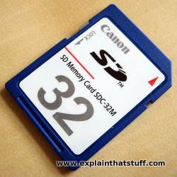
Flash memory eventually wears out because its floating gates take longer to work after they've been used a certain number of times. It's very widely quoted that flash memory degrades after it's been written and rewritten about "10,000 times," but that's misleading. According to a 1990s flash patent by Steven Wells of Intel, "although switching begins to take longer after approximately ten thousand switching operations, approximately one hundred thousand switching operations are required before the extended switching time has any affect on system operation." Whether it's 10,000 or 100,000, it's usually fine for a USB stick or the SD memory card in a digital camera you use once a week, but less satisfactory for the main storage in a computer, cellphone, or other gadget that's in daily use for years on end. One practical way around the limit is for the operating system to ensure that different bits of flash memory are used each time information is erased and stored (technically, this is called wear-leveling), so no bit is erased too often. In practice, modern computers might simply ignore and "tiptoe round" the bad parts of a flash memory chip, just like they can ignore bad sectors on a hard drive, so the real practical lifetime limit of flash drives is much higher: somewhere between 10,000 and 1 million cycles. Cutting-edge flash devices have been demonstrated that survive for 100 million cycles or more.
Who invented flash memory?
Flash was originally developed by Toshiba electrical engineer Fujio Masuoka, who filed US Patent 4,531,203 on the idea with colleague Hisakazu Iizuka back in 1981. Originally known as simultaneously erasable EEPROM (Electrically Erasable Programmable Read-Only Memory), it earned the nickname "flash" because it could be instantly erased and reprogrammed—as fast as a camera flash. At that time, state-of-the-art erasable memory chips (ordinary EPROMS) took 20 minutes or so to wipe for reuse with a beam of ultraviolet light, which meant they needed expensive, light-transparent packaging. Cheaper, electrically erasable EPROMS did exist, but used a bulkier and less efficient design that required two transistors to store each bit of information. Flash memory solved these problems.
Toshiba released the first flash chips in 1987, but most of us didn't come across the technology for another decade or so, after SD memory cards first appeared in 1999 (jointly supported by Toshiba, Matsushita, and SanDisk). SD cards allowed digital cameras to record hundreds of photos and made them far more useful than older film cameras, which were limited to taking about 24–36 pictures at a time. Toshiba launched the first digital music player using an SD card the following year. It took Apple a few more years to catch up and fully embrace flash technology in its own digital music player, the iPod. Early "classic" iPods all used hard drives, but the release of the tiny iPod Shuffle in 2005 marked the beginning of a gradual switchover, and all modern iPods and iPhones now use flash memory instead.
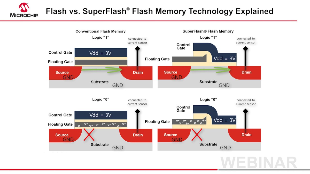
SuperFlash® Technology

SuperFlash® technology is an innovative and versatile type of NOR Flash. SuperFlash technology uses a proprietary split-gate cell architecture which provides superior performance, data retention, and reliability over conventional stacked gate Flash.
Flash memory form factors
Flash-based media is based on a silicon substrate. Also known as solid-state devices, they are widely used in both consumer electronics and enterprise data storage systems.
There are three SSD form factors that have been identified by the Solid State Storage Initiative:
- SSDs that fit into the same slots used by traditional electromechanical hard disk drives (HDDs). SSDs have architecture similar to that of an integrated circuit.
- Solid-state cards that reside on a printed circuit board and use a standard card form factor, such as Peripheral Component Interconnect Express (PCIe).
- Solid-state modules that fit in a dual inline memory module (DIMM) or small outline dual inline memory module using a standard HDD interface, such as the Serial Advanced Technology Attachment (SATA).
An additional subcategory is a hybrid hard drive that combines a conventional HDD with a NAND flash module. A hybrid hard drive is generally viewed as a way to bridge the divide between rotating media and flash memory.
All-flash and hybrid flash memory
The advent of flash memory fueled the rise of all-flash arrays. These systems contain only SSDs. They offer advantages in performance, and sometimes reduced operational costs, compared to all disk-based storage arrays. The chief difference, aside from the media, is in the underlying physical architecture used to write data to a storage device.
HDD-based arrays have an actuator arm that enables data to be written to a specific block on a specific sector on the disk. All-flash storage systems do not require moving parts to write data. The writes are made directly to the flash memory, and custom software handles data management.
A hybrid flash array blends disk and SSDs. Hybrid arrays use SSDs as a cache to speed access to frequently requested hot data, which subsequently is rewritten to back-end disk. Many enterprises commonly archive data from disk as it ages by replicating it to an external magnetic tape library.
Flash plus tape, also known as flape, describes a type of tiered storage in which primary data in flash is simultaneously written to a linear tape system.
In addition to flash memory arrays, the ability to insert SSDs in x86-based servers has increased the technology's popularity. This arrangement is known as server-side flash memory and it enables companies to sidestep the vendor lock-in associated with purchasing expensive and integrated flash storage arrays.
The drawback of placing flash in a server is that customers need to build the hardware system internally, including the purchase and installation of a storage management software stack from a third-party vendor.
Pros and cons of flash memory
Flash is the least expensive form of semiconductor memory. Unlike dynamic random access memory (DRAM) and static RAM (SRAM), flash memory is nonvolatile, offers lower power consumption and can be erased in large blocks. Also, on the plus side, NOR flash offers fast random reads, while NAND flash is fast with serial reads and writes.
An SSD with NAND flash memory chips delivers significantly higher performance than traditional magnetic media, such as HDDs and tape. Flash drives also consume less power and produce less heat than HDDs. Enterprise storage systems equipped with flash drives are capable of low latency, which is measured in microseconds or milliseconds.
The main disadvantages of flash memory are the wear-out mechanism and cell-to-cell interference as the dies get smaller. Bits can fail with excessively high numbers of program/erase cycles, which eventually break down the oxide layer that traps electrons. The deterioration can distort the manufacturer-set threshold value at which a charge is determined to be a zero or a one. Electrons may escape and get stuck in the oxide insulation layer, leading to errors and bit rot.
Anecdotal evidence suggests NAND flash drives are not wearing out to the degree once feared. Flash drive manufacturers have improved endurance and reliability through error correction code algorithms, wear leveling and other technologies.
In addition, SSDs do not wear out without warning. They typically alert users in the same way a sensor might indicate an underinflated tire.
NAND flash memory storage types
NAND flash semiconductor manufacturers have developed different types of memory suitable for a wide range of data storage uses cases. The following chart explains the various NAND flash types.
Types of NAND flash memory storage
| ||||
Description
|
Advantages
|
Disadvantages
|
Primary use
| |
Stores one bit per cell and two levels of charge.
|
Higher performance, endurance and reliability than other types of NAND flash.
|
Higher cost than other types of NAND flash.
|
Enterprise storage, mission-critical applications.
| |
Can store multiple bits per cell and multiple levels of charge. The term MLC equates to two bits per cell.
|
Cheaper than SLC and enterprise MLC (eMLC), high density.
|
Lower endurance than SLC and eMLC, slower than SLC.
|
Consumer devices, enterprise storage.
| |
Typically stores two bits per cell and multiple levels of charge; uses special algorithms to extend write endurance.
|
Less expensive than SLC flash, greater endurance than MLC flash.
|
More expensive than MLC, slower than SLC.
|
Enterprise applications with high write workloads.
| |
Stores three bits per cell and multiple levels of charge. Also referred to as MLC-3, X3 or 3-bit MLC.
|
Lower cost and higher density than MLC and SLC.
|
Lower performance and endurance than MLC and SLC.
|
Mass storage consumer applications, such as USB drives, flash memory cards, smartphones, and client SSDs, and data center SSDs for read-intensive workloads.
| |
Vertical/3D NAND
|
Stacks memory cells on top of each other in three dimensions vs. traditional planar NAND technology.
|
Higher density, higher write performance and lower cost per bit vs. planar NAND.
|
Higher manufacturing cost than planar NAND; difficulty in manufacturing using production planar NAND processes; potentially lower data retention.
|
Consumer and enterprise storage.
|
*Quad-level cell (QLC)
|
Uses a 64-layer architecture that is considered thenext iteration of 3D NAND. Not widely available as of November 2017.
|
Stores four bits of data per NAND cell, potentially boosting SSD densities.
|
More data bits per cell can affect endurance; increased costs of engineering.
|
Mostly write once, read many (WORM) use cases.
|
Note: NAND flash wear-out is less of a problem in SLC flash than it is in less expensive types of flash, such as MLC and TLC, for which the manufacturers may set multiple threshold values for a charge. The commonly cited industry wear-out figures are 100,000 program/erase -- write/erase -- cycles for SLC NAND flash; 30,000 for eMLC; 10,000 or fewer for MLC; and 3,000 or fewer for TLC. Actual endurance figures may be higher.
* Samsung and Western Digital have disclosed or previewed preliminary designs for their respective QLC architectures.
| ||||
Vendor breakdown of enterprise NAND flash memory products
Major manufacturers of NAND flash memory chips include Intel Corp., Micron Technology Inc., Samsung Group, SanDisk Corp. -- now owned by Western Digital Corp. -- SK Hynix Inc. and Toshiba Memory Corp.
A NAND flash shortage is causing disruption in the market. The shortfall is causing SSD prices to rise and lead times to lengthen. The demand outstrips supply largely due to soaring demand from smartphone makers.
Other turmoil is exerting an impact on the market. As of November 2017, leading flash supplier Toshiba agreed to sell its chip making unit to a group of corporate and institutional investors led by Bain Capital. Toshiba sold the flash business as part of its effort to cover financial losses and to avoid being delisted on the Tokyo Stock Exchange.
However, Toshiba partner Western Digital (WD) has vowed to fight the $18 billion deal. WD inherited a stake in Toshiba's chip business following its acquisition of SanDisk Corp., which had a joint venture with Toshiba.
NOR flash memory types
The two main types of NOR flash memory are parallel and serial, also known as serial peripheral interface. NOR flash was originally available only with a parallel interface. Parallel NOR offers high performance, security and additional features; its primary uses include industrial, automotive, networking, and telecom systems and equipment.
NOR cells are connected in parallel for random access. The configuration is geared for random reads associated with microprocessor instructions and to execute codes used in portable electronic devices, almost exclusively of the consumer variety.
Serial NOR flash has a lower pin count and smaller packaging, making it less expensive than parallel NOR. Use cases for serial NOR include personal and ultra-thin computers, servers, HDDs, printers, digital cameras, modems and routers.
Leading NOR vendor products
Major manufacturers of NOR flash memory include Cypress Semiconductor Corp. -- through its acquisition of Spansion Inc. -- Macronix International Co. Ltd., Microchip Technology Inc., Micron Technology Inc. and Winbond Electronics Corp.
Cypress Semiconductor acquired NOR flash provider Spansion in 2015. The Cypress NOR portfolio includes FL-L, FL-S, FS-S and FL1-K products.
Macronix OctaFlash uses multiple banks to enable write access to one bank and read from another. Macronix MX25R Serial NOR is a low-power version that targets internet of things (IoT) applications.
Microchip NOR is branded as Serial SPI Flash and Serial Quad I/O Flash. The vendor's parallel NOR products include the Multi-Purpose Flash devices and Advanced Multi-Purpose Flash devices families.
Micron sells Serial NOR Flash and Parallel NOR Flash, as well as Micron Xccela high-performance NOR flash for automotive and IoT applications.
The Winbond serial NOR product line is branded as SpiFlash Memories and includes the W25X and W25Q SpiFlash Multi-I/O Memories. In 2017, Winbond expanded its line of Secure Flash NOR for additional uses, including system-on-a-chip design to support artificial intelligence, IoT and mobile applications.
The future of the flash memory market
The flash memory market continues to see advances in form factor and deployment options. Storage array vendors are adding support for the nonvolatile memory express (NVMe) controller interface, a protocol that accelerates data transfer between client systems and flash storage. An NVMe host controller exploits the high-speed performance of the PCIe bus.
Using PCIe enables an application to communicate directly with flash storage by reducing network hops that would occur with host bus adapters and routers. PCIe enables the emergence of drives built on the NVMe specification, providing an alternative that experts believe could supplant 2.5-inch and 3.5-inch form factors. NVMe SSDs plug into idle server slots on a computer, removing the cost and complexity associated with cabling.
Rising with NVMe and PCIe-connected SSDs are nonvolatile dual inline memory modules (NVDIMMs) that integrate DRAM, NAND flash and a dedicated backup power supply. NVDIMMs may be inserted in a standard DIMM connector on a memory bus. The flash memory on an NVDIMM card serves to back up and restore data kept in DRAM, while the onboard power supply ensures the storage remains nonvolatile.
Candidates to succeed NAND flash have emerged. In fact, some of these memories have been in development for a while. These alternative technologies are based on memory architectures that differ from NAND's floating gate transistor.
Phase change memory (PCM) stores data by changing the state of the bit cell using electrical pulses. These pulses alter the nonvolatile DRAM from an unstructured to a structured state. Potential advantages of PCM include lower latency on read data and accelerated write performance. In addition, PCM enables an individual byte to be written, whereas flash memory requires an entire block of data to be written.
Resistive random access memory, known also as ReRAM or RRAM, is nonvolatile storage that bears similarities to PCM. Instead of electrical pulses, ReRAM changes the resistance properties of the underlying dielectric, which can include various oxide metals and other solid materials. A ReRAM device includes a nonvolatile memory resistor, or memristor, which is a component that regulates a circuit's electricity flow and retains information on the amount of charge that has flowed through it historically.
In comparison with NAND, ReRAM is said to offer higher switching speed and lower power consumption. 4DS Memory Ltd., Crossbar Inc., Fujitsu Semiconductor, Israeli startup Weebit Nano and Western Digital -- through SanDisk ReRAM -- are all working to bring ReRAM-based storage products to market. Hewlett Packard Enterprise dropped its Memristor product in 2016, after experimenting with it in joint ventures with SanDisk and SK Hynix.
Magneto-resistive RAM (MRAM) stores data using magnetic states. A pair of ferromagnetic metal plates is used: one plate is a permanent magnet and a second plate is capable of being magnetized. Separating the two plates is a thin layer of insulating material. Binary bits are defined as one or zero according to the orientation of the two magnetic fields.
A related approach is spin-torque transfer, a method that sends an electric current to thin magnetic layers situated between non-magnetized materials. The current alters the spin of electrons to an up or down state.
the devices being integrated with an interface that is a USB. They are very convenient due to their small size and weight and the fact that they are both rewritable and removable. These drives are available with different storage limits ranging from usually 4GB to 64GB.
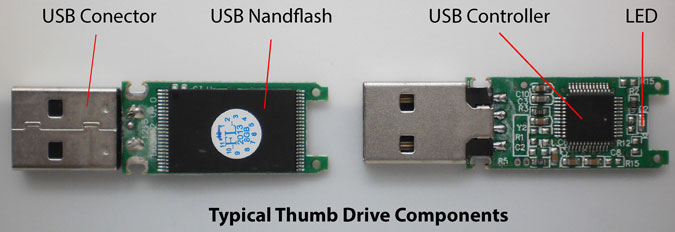
There are a number of advantages of using a thumb drive as opposed to the now antiquated floppy disc. They are smaller, more reliable, rarely break due to the lack of moving parts, and they can hold more data and are faster too. Inside a thumb drive you will find a circuit board; this board is printed and encased in a tough metal or plastic exterior, meaning you can carry it around in your bag or pocket. There is generally a removable cap on the end that protects the protruding USB connector. The vast majority of flash drives can be connected directly to your PC through a standard USB connector.
The USB connection provides the power supply for the flash drive, meaning that it needs no other external source of power and will work when simply connected to the USB of your computer or other device. You need to connect your flash drive to your computer via a USB port or HUB in order to read the data that is saved on it.
The very first USB flash drive that was created was an 8MB version that was known as the 16 megabyte “disgo”. Dov Moran, CEO and president of M-System Flash Pioneers invented the very first flash drive in 1998. The now Vice President of SanDisk, Dan Harkabi led the marketing and development of the drive at M-Systems. The most significant advance made by him was the development of a flash drive that did not need you to install any drivers to use it. Trek 2000 and Netac also undertook simultaneous developments, creating very similar products. These three companies all patented their devices, the patents being disputed at the time. The first flash drive to be sold was in the US, the drive being sold in 2001 under the name “Memory key”. The drive had an 8MB capacity. Later on, Trek 2000 manufactured a 16MB version that was introduced onto the market by IBM; then in 2003 the 64MB version was to be introduced by M-Systems. Lexar is another company that can lay claim to a flash or thumb drive. In 2000, Lexar were to produce a CF (Compact Flash) card that had an internal USB. This product eliminated the need for a USB as it was offered with a USB cable and a companion card reader.
The first thumb or flash drives that were to be sold in Europe were sold under the “disgo” name, and they were made by M-Systems in sizes of 8, 16, 32, and 64MB. This product was marketed to kill the floppy disc for good, and the largest capacity to be introduced onto the market was 256MB. After the introduction of flash drives in Europe, cheaper alternatives would then appear onto the Asian market.
The first thumb or flash drives that were to be sold in Europe were sold under the “disgo” name, and they were made by M-Systems in sizes of 8, 16, 32, and 64MB. This product was marketed to kill the floppy disc for good, and the largest capacity to be introduced onto the market was 256MB. After the introduction of flash drives in Europe, cheaper alternatives would then appear onto the Asian market.
A modern flash drive has a USB2.0 connectivity. However, although systems will support a 480 Mbit/s drive, technical limitations in the NAND flash mean that this limit is never actually reached.
Everywhere you look nowadays you will see flash drives that include business logos and are printed and made in many different designs. Flash drives have mean that businesses have been able to reach their real branding objectives, the promotion merchandise being heavily successful. When you own a flash drive, you can simply save and transport your files and data wherever you go. A business can promote itself to anyone, anywhere; all that is necessary is a USB port. Businesses are even able to offer further services such as providing catalogs, discount vouchers, and promotional materials on their pen drives. They can include huge amounts of electronic data on their drives, providing huge success for them wherever they go.
Since the first introduction of the flash drive, the growth has been extremely quick, and both the quality and quantity have increased. Businesses began to make bulk order of flash or thumb drives; this meant that they could save both time and financial resources. Also, the quality of flash drives has improved immensely since they were first introduced, and there is a wide range of capacities available to meet the different demands of the consumer. Some people require a small drive such as an 1GB drive for personal use; others need 32GB or more for their business requirements. As well as choosing from different storage amounts, businesses can also choose promotional flash drives to promote their brand, the storage limitations being unimportant in this case. As well as flash drives and thumb drives, businesses have also being developing USB watches and pens; in these cases the development has been geared more to design and fashion rather than to the actual capacity of the drive.
USB 2.0 Hi-speed Flash drive
Whether you refer to it as a pen drive, jump drive, thumb drive, key drive, or memory stick, you have to admit, the USB Flash drive is pretty darn cool. Just stick it into the USB port on your computer and within a few seconds a new drive appears on your desktop. So simple and so easy. What makes them so good is that they have a spate of desirable features such as no need for batteries, solid state storage, good transfer speeds, durability, portability, and expected data retention of ten years. All of these features allow these little babies to practically replace the floppy, the Zip disk, and the CD-R/RW all in one fell swoop.
Unfortunately, when comparing USB Flash drives side-by-side in a computer or electronics store, it can be awfully difficult to decide which is best for you just by looking at the drive and the packaging. It would be easy to make an assumption that all drives are pretty much the same and that shopping for the best price is the smartest way of deciding. We are here to inform you that USB Flash drives are not a commodity and can be very unique offerings. As you will soon find out, some are clearly better than others while others come bundled with nifty features that can really make your day. In short, not all flash drives are created equal.


Products (left to right)
- Fujifilm USB drive - 128MB (US$62 — shop for this drive)
- Iomega Mini - 128MB (US$60 — shop for this drive)
- Mushkin Flashkin - 128MB (US$46)
- PNY Attache - 128MB (US$60 — shop for this drive)
- Transcend JetFlash2A - 128MB (US$38 — shop for this drive)
- SanDisk Cruzer Mini - 128MB (US$31 — shop for this drive)
- Verbatim Store 'n' Go - 256MB (US$85 — shop for this drive)
- SimpleTech Bonzai Xpress - 256MB (US$80 — shop for this drive)
Background on the Universal Serial Bus (USB)
Back in 1995, it was becoming quite clear that the serial and parallel ports on the PC were outliving their usefulness. While Ethernet was becoming generally available, it was still rather expensive to implement and not all devices needed to be shared on a Local Area Network. Thus it was deemed that a new serial bus should be designed to take on the role of the old serial and parallel ports. By January of 1996, USB 1.0 was born. The new serial bus protocol supported two signaling rates: low speed (1.5Mbps) and high speed (12Mbps) Unfortunately, there was practically no operating system support and virtually no hardware available with which to operate. Microsoft, ultimately, did create OEM versions of Windows 95 with USB support, but the support written in was barely usable.
In May 1998, Apple released the original Bondi Blue iMac, which was the first personal computer to completely abandon legacy ports in favor of USB. Microsoft released Windows 98 that year with much better USB support and by September a new revision of USB (version 1.1) was released. Increasing numbers of USB devices started to hit the market and made certain that USB was here to stay. Unfortunately, it quickly became evident that 12Mbps was not enough throughput for devices like CD writers and external Hard drives. By 2000, USB 2.0 was created with a theoretical data transfer rate of 480Mbps. With the 14-fold speed increase, USB became a viable option for fast, portable storage devices.
 Unfortunately, the phrase "USB 2.0" does not necessarily mean 480Mbps of throughput. USB 2.0 now has three different signaling rates: Low Speed (1.5Mbps), Full Speed (12Mbps), and Hi-Speed (480Mbps). The marketing and advertising departments of product manufacturers like to put the words "USB 2.0" on all of their product packages. This can be really deceptive since most consumers will see USB 2.0 and compare it to an older product with the USB 1.1 moniker and think "USB2 must be better than USB 1.1!" Naturally, the consumer is unaware of the difference between "Full Speed" and "High Speed" (this is something akin to the old naming snafu with floppy disks: does "double density" or "high density" hold more?).
Consequently, as a warning to the reader by mentioning that if it does not say "USB 2.0 Hi-Speed" or does not feature the logo on the left, it ain't very fast. All the drives found in this review are USB 2.0 Hi-Speed drives. While USB 1.1 (a.k.a. USB 2.0 Full-Speed) drives still exist, the price of Hi-Speed USB 2.0 drives have come down so much recently that there is no really good reason to consider the slower drives. For the sake of comparison, benchmark scores from one such drive are included in this review.
How we tested
Each drive was evaluated on several factors:
- Features
- Accessories
- Extras
- Construction
- Software
Each drive was tested in a variety of scenarios as well as on different operating systems such as Win98, Win2000/XP, and Mac OS X. We tested on various kinds of hardware and USB hubs. We carried each drive around and gave them a fair amount of real world use to see how each would hold up to the rigors of daily usage. The following systems were used for the majority of our testing:
Macintosh test system
PowerBook G4 1.33Ghz
512MB DDR RAM 80GB Fujitsu HDD Mac OS X 10.3.3 | PC system
AthlonXP 3200+ (2.2Ghz)
512MB PC3200 DDR RAM 120GB WD1200JB HDD Windows XP SP1 |
To round things out, we benchmarked each USB Flash drive using various applications. For Windows, we used SiSoft Sandra 2004.2.9.104. On the Mac, we used SpeedTools QuickBench program. We also used a “stop-watch” Perl script in Windows to replicate the Sandra write-performance benchmarks as well as create custom benchmarks. This combination of benchmarking across platforms allowed us to get a good picture of performance on each drive and each platform.
Common features, accessories, and extras
 |
Neck strap with quick release: Most of the drives here feature a neck strap with the exact same quick-release snap. As shown on the left, by pinching the snap, the drive is able to detach from the neck strap. While some may not find the neck strap very useful, it is a nice addition for others.
|
 |
USB extension cable: Virtually all computers come equipped with USB ports these days, but there are still a large number of machines that have no USB ports on the front of the case. If the only available ports are in the back, plugging and unplugging USB drives can be a pain. The simplest solution to this problem is a three-foot extension cable. Some manufacturers have been thoughtful enough to include one with their drive offering.
|
 |
Write-protect switch: Just like the floppy disk, some Flash drives contain write-protect switches. The obvious benefit of the write-protect switch is to prevent the accidental deletion or overwriting of files. This is particularly advantageous to the system administrator who is trying to disinfect a machine that has somehow contracted a worm or virus; just carry the write-protected USB drive with the anti-virus software to the infected machine and never worry about the Flash drive becoming compromised. Perhaps the best thing about the write-protect switch is that, unlike the floppy, write-protection can be turned on and off without needing to remove the drive from the USB port.
|
 |
Security/password protection software and driver software: All USB drives have Win98 drivers available. Some come on full-size CDs, others come on the mini CDs, while others are only available for download from the company website. Windows ME/2000/XP all have native support for USB Mass Storage devices as does Mac OS 9, OS X, and Linux 2.4.2+. (Windows 95 does not appear to have support, but Mac OS 8.6 has drivers available for download from Apple's site.) Many drives also have security/password protection or file synchronization software on CD or are available free for download.
|
 |
Low power support, boot support, and warranty: Considering how small most of these drives are, it might be logical to think that they use little power, but unfortunately, some use more power than an unpowered USB hub can provide. About half the drives in this review worked fine, while the other half did not. For some people this may be an issue (Mac users with USB keyboards: please take note!) Some of these drives are also able to masquerade as USB-based ZIP or Hard drives allowing them to boot at startup. For most people this is a useless feature, but for most geeks and system administrators, this could be really worthwhile. Although few manufacturers listed the MTBF for their drives, all carry at least a 1-year warranty, with a few offering 2-year, 3-year, and Lifetime warranties.
|
Meet the contenders
PNY Technologies Attaché

Features
|
Construction: The PNY Attaché drive enclosure is made entirely of plastic, yet feels solid in the hand. The rectangular shape and the smooth corners make it feel pretty normal as USB drives go. Some people will find the colored transparent casing interesting as it allows viewing of the components on the inside. The protective cap stays firmly fixed on the end of the drive but is not difficult to remove. The only questionable aspect of this drive's construction is that the blue transparent part of the drive pulls out from the larger silver plastic piece. While not a show stopper, it seemed strange that the two pieces of plastic were not permanently joined together.
The PNY Attaché features a red LED on one side of the drive to indicate that the unit is plugged in and operational. The LED flashes when data is being transferred. This drive contains a plastic loop to attach to a lanyard or key ring for your keychain. It also includes a write-protect switch to prevent accidental overwriting/deletion of files. The switch is counter-sunk, so a pen or similar tool is needed to flip the switch. Alternatively, it is possible to pull the blue transparent center part out of the silver plastic part and flip the switch with a fingernail and then merge the two parts back together.
Software: The Attaché includes a mini CD with only a driver for Windows 98 SE users. No other software is included.
SanDisk Cruzer Mini

Features:
|
Construction: The SanDisk Cruzer Mini drive is made entirely of plastic. While it does not feel as solid is some other drives made of thicker plastic, it definitely feels durable to withstand the rigors of daily life. The Cruzer Mini is a rather svelte drive, as USB Flash drives go. From the picture on the left, it should be evident that the drive is about as thick as the USB port on your computer. While some might argue that the drive is a bit too thin, it is easy to recognize that this drive definitely does not block access to dual-stacked USB ports found on many computers. The Cruzer Mini is one of the four drives that are "low power" (i.e. work in unpowered USB hubs and USB keyboards.) The Cruzer Mini also comes with 3 different colored caps that snap on pretty securely.
The SanDisk Cruzer Mini features a bright, green LED on the end of the drive that can be seen from nearly any angle (really smart!) The LED flashes when transferring data and turns off when the OS is no longer accessing the drive. The drive has a small loop for a lanyard string to pass through. Unfortunately, this little loop is really small and is kind of like trying to thread a needle. We have also witnessed this thin little plastic loop break under moderate stress. The current revision of the Cruzer Mini has NO write-protect switch, although older, thicker models have this feature. SanDisk probably dropped this feature when attempting to make the drive thinner. Unfortunately, for some people, this is a useful feature to have.
Software: The packaging does NOT include a CD-ROM with software, but the Win98 drivers and the CruzerLock security software are both available on their website for download.

CruzerLock
The CruzerLock software looks and behaves much like Windows Explorer. The difference is that the files that you view on the drive are either decrypted or encrypted. As shown in the picture, there are three text files and the CruzerLock software in the unencrypted folder and a "contacts" file that is encrypted. Unfortunately, we were unable to ascertain the type and strength of encryption. In addition, we found it odd that the software would allow us to encrypt the CruzerLock executable itself. This becomes problematic the next time the drive is inserted. Obviously, the decrypt/encrypt software cannot run if it is encrypted and thus all the encrypted files are rendered useless (unless a local copy of the CruzerLock software is available.) That aside, the encryption and decryption seemed to take place rather quickly, even on a 1Ghz machine.
Mushkin Flashkin

Features:
|
Construction: The Mushkin Flashkin drive is made almost entirely of plastic with exception to the metal clip on the cap. The smooth, egg-like shape of the Flashkin feels nice in the hand, yet the plastic is thin enough that it is pretty clear that the drive case is a good deal larger than the actual components inside. It is unfortunate that the drive enclosure is so oversized since the drive somewhat blocks dual-stacked USB ports found on most computers. The drive is held together by one small screw. Given the opportunity, we decided to take a look inside and examine the innards.
The Mushkin Flashkin drive features a small ,but bright red LED on one side that flashes when transferring data. The Flashkin has a small loop on the end of the drive for a lanyard or key ring. The metal clip on the cap is somewhat useful if you plan on carrying it in a shirt pocket. If not, you can always remove the clip by unscrewing the retention screw underneath the cap. The Flashkin has a write protect switch that flips without any difficulty, yet has enough friction to stay switched in the direction that it is set at. It is one of the four drives that are "low power" (i.e., works in unpowered USB hubs and keyboards.)
Software: The package includes a mini CD with Win98 SE drivers as well as software for enabling password protection and boot support.

Want to boot from your Flashkin?
The Mushkin security and support software appears very Spartan and simplistic on the surface. While not very pretty, it is actually rather functional. The software allows the user to set/change/clear the password, partition the device into a public and private area, and even copy system boot files onto the drive (if you are running on Win98/Me.) A common problem with USB Flash drives is that sometimes after partitioning/reformatting using Windows tools, the drive actually shrinks in overall usable size by a few MB. Fortunately, Mushkin includes a format utility which allows full recovery of all the available space.
As shown above, the available drive space can be partitioned into two drives: a "public" drive which can be accessed by anyone and a "private" drive which can only be accessed with the right password. The drive can also be put into one of three different possible boot modes.
More contenders
SimpleTech Bonzai Xpress

Features:
|
Construction: The SimpleTech Bonzai Xpress has the best construction design of all the USB drives in this review. The enclosure is made mostly of texturized, durable black plastic which has a good, almost rubbery feel in the hand. The side walls of the drive are made of aluminum, making it extra sturdy. The ridges on the black part of the drive make it especially easy to grasp. It is neither too large nor too small and is just about the right thickness so as not to obstruct dual-stacked USB ports.
The SimpleTech Bonzai Xpress drive features a small LED on one side that flashes just like every other drive when transferring data. The aluminum loop on the end is clearly large enough to loop a neck strap through and strong enough to put on a keychain. The Bonzai Xpress has a write-protect switch that is easily moved, yet has enough friction to stay in place.
Software: Downloadable storage synchronization software comes standard. For a small fee, this standard StorageSync software is upgradeable to a professional edition which features 2:1 software compression, 128, 192, and 256-bit AES encryption, and a 20-deep file revision tracking system.

StorageSync
While we did not purchase a copy of the professional edition, we did test the synchronization software extensively. Overall, we were rather satisfied with the program. It was easy to figure out that in order to synchronize the data between the hard drive and the flash drive, we needed to "backup" the data first. Pretty easy. The big question: how well does the program sync the data? We started by creating a text file and then backed it up so that it would be the same on both the hard disk and flash drive. We then altered the file in both locations to be two different files. It appears that the newer file always overwrites the older file. If you do not understand this, you may get yourself into trouble, especially if there are two people doing work on the same file. More recent changes may overwrite the changes that someone else made earlier. Apparently, to get file revision tracking, you need to purchase the professional upgrade.
We did note one minor caveat and a more serious annoyance. The small problem was that instead of "My Documents" being readily available under the root of the file/directory menu, we had to drill down through "Documents and Settings" then "Username" then "My Documents." A minor quibble, but an irritating oversight nonetheless. The more serious annoyance was that the program only seemed able to pick up changes to already-backed-up files. Any new files created on the Flash drive's backup directory or the hard disk's backed up folders were completely missed. This is somewhat frustrating since most people not only change files, but frequently create new files and folders. Scanning for new files as well as changes to old ones seems like a no-brainer. Since SimpleTech has a software update system, hopefully they will pick up on this problem and fix their StorageSync software.
Fujifilm USB Drive 2.0

Features:
|
Construction: The Fujifilm USB Drive 2.0 is made entirely of plastic and is a tad long, as USB drives go. Overall, it feels comfortable in the hand. The oddest thing about the construction of this drive is that the loop for the keychain/neck strap is not a closed loop. In fact, it is a cross between a shirt pocket clip and a loop for a thicker strap. Incidentally, the drive does NOT come with a neck strap. The "open loop" was a little unnerving, not only because it seemed really easy for the drive to come off a neck strap, but also because the loop was connected to the drive's cap and not the drive itself. Admittedly, we could see the ease of use in being able to pull the drive out from the cap while keeping the cap hanging around one's neck, but frankly it seemed too easy to lose. We would much rather lose the cap, than the drive itself.
The Fujifilm USB Drive drive features both an orange and green LED that shine brightly through the translucent blue plastic. The LED glows green when in Full-Speed mode (12Mbit/sec) and orange when in Hi-Speed mode (480Mbit/sec). Like all other drives, the LED flashes when transferring data, but when sitting idle, the LED slowly fades in and out like an iMac in sleep mode. Very cool! The LED can also been seen from both sides of the drive.
Software: Available for download are the Win98 driver and Fujifilm's own Sentinel security software for password protection and public/secure partitioning of the drive.

Sentinel, at your service!
The software for the Fujifilm drive is straightforward and the software executes from the public partition of the drive. The only thing that was a tad annoying was that it was not possible to have both the public and private partitions available simultaneously. The only option was either to be "logged in" (using the private partition) or "logged out" (using the public partition). For the most part, this is not a problem, but when moving data between the public and private partitions, it does force the user to move data to the host's hard drive temporarily.
Final contenders
Verbatim Store 'n' Go

Features:
|
Construction: The Verbatim Store 'n' Go is made almost entirely of transparent plastic. The drive is rather small in comparison to all the other drives in this review. Like the Fujifilm drive, the keychain/neck strap loop is on the cap rather than the body of the drive itself. While we can see the advantage of being able to quickly yank the drive out from the cap, it is still a little unsettling that it would be easier to lose the drive rather than the cap. Despite this, the drive feels solid in hand and has 3 raised dots on the body to give better friction for handling the device.
The Verbatim Store 'n' Go features an LED that flashes when transferring data just like every other drive. The plastic loop on the cap is clearly large enough to handle either a neck strap or a keychain. Unfortunately, the drive has no write-protect switch, but just like the SanDisk, this was probably done to help keep the drive small.
Software: The package includes a mini CD with Win98 SE driver as well as software for password protection and public/secure partitioning of the drive.

Ready to Store 'n' Go!
The Verbatim Store 'n' Go software is very well done and has a lot of polish to the controls. Creating a public/secure area is a breeze and password protecting the drive is just as easy. The only thing we did not like about it was that instead of running as an executable from the public area, the software has to first unpack from an Install Shield Wizard and then install on every computer that you need to work on. When moving between computers, this really slows things down. Additionally, if the user lacks proper machine permissions (common in an office environment), the install may fail. Interestingly enough, the software also appears to not have any "boot support."
Transcend JetFlash 2A

Features:
|
Construction: The Transcend JetFlash 2A is made of both silver and colored, transparent plastic. The drive is medium-sized in comparison to the other drives, yet feels pretty solid. The cap attaches firmly to the drive and on the end of the drive is a small loop just large enough for the neck strap thread to pass through. The Transcend JetFlash 2A features an LED that flashes when transferring data and has a nice transparent window so that the inner components are somewhat visible. The JetFlash also has a write-protect switch on the side which slides without any difficulty and stays in place when moved. Unfortunately, the switch is unlabeled, so it is not immediately obvious which position is "write-protect" and "write-enable." The good news is that the Transcend JetFlash is one of the four drives that are "low power" (i.e., work in unpowered USB hubs and USB keyboards.)
Software: On the included (full-size) CD-ROM is the Win98 driver and Transcend's own security software.

A Transcendent application?
As shown, the Transcend has a simple, but easy-to-use interface that allows formatting, drive partitioning, boot enabling, and password protection all on one screen. (Very slick!) The software for accessing the drive is also carried in the public directory of the drive and runs directly from the drive. Being able to reconfigure the device without having to reformat the drive was a really nice touch.
Iomega Mini Drive

Features:
|
Construction: The Iomega Mini Drive is built mostly of plastic, but feels strong. The metal loop that swings on the cap, locks onto the body to hold the cap in place. The LED is thoughtfully placed on the end of the drive for viewing from nearly any angle. Unfortunately, the LED is rather dim and thus difficult to see. It is also one of the "low power" drives in our review. One of the nicest features about this drive is that it has a slot to insert your own custom label. This can be particularly useful if you have a few of them or you do not want yours getting confused with a co-worker's drive.
Software: Iomega has a software technology called Active Disk. Active Disk gives the user the ability to run certain applications directly from the Iomega drive of choice (this could be a Zip disk or a USB Flash drive.) When we say "certain" applications, we mean only applications that have been tailored to work with Active Disk will work properly. So what sort of software runs with Active Disk? On the Mac side, there is MacWasher, Simple Journal, as well as a handful of games. On the Windows side, the most popular titles are OpenOffice, VNC, IrfanView, MusicMatch Jukebox, as well as Iomega's own Sync software. When we tested Iomega Sync we were unable to get it to work with our USB Flash drive for some reason. (Our evaluation unit might have been defective.) But we were able to test it with a ZIP disk and drive. We found that Iomega Sync synchronizes files, gracefully handles file conflicts, automatically synchronizes files while the removable drive is still attached, and it even adds files to the Sync Set that were not previously there. (Unlike the SimpleTech software.) Also found on Iomega's site is a software package called SmartLogin which offers password protection and public/private partitioning, much like the other drives in the review.
Read performance benchmarks
Before we begin, we wanted to mention again that all the drives in this review are USB 2.0 Hi-Speed drives. Although these drives do not utilize all the bandwidth of USB 2.0 (480Mbps), all of these drives perform better than any USB 1.1 Flash drive. So just by merit of being a USB 2.0 Hi-Speed drive, each one is much faster than any USB 1.1 drive. That said, it would be easy to think that all the drives in this review perform the same, but of course, this is not the case. Some are clearly better than others.
The results for the PC platform were widely varied. SiSoft Sandra gives only a few data points, but shows that each drive performs differently from the next.

As shown in the graph, all drives start off rather slow at the rather small file size of 512 bytes. The slowest drive out of the gates was the SanDisk drive averaging 210KB/sec. The fastest was the Iomega drive moving lots of 512-byte files at an average of 552KB/sec, trailed closely by the Fuji drive at 535KB/sec and the SimpleTech and Transcend drives at 495KB/sec. Compared to the ZIP100 (25KB/sec) and the USB 1.1 drive (75KB/sec), these drives are fast. Although, just by looking at the graph it should be clear that there is a throughput penalty for dealing with such small bursts of data since none of the drives were even close to their rated read speeds.
Progressing to 32KB, 256KB, and 2MB file sizes really allowed these drives to show their stuff. The fastest drives at reading are the Fujifilm, Transcend, and Iomega. All three consistently averaged throughput in the 8 to 10MB/sec range. The next fastest group is comprised of the SanDisk, SimpleTech, and the Verbatim drives. Those three showed strong throughput in the 6 to 8MB/sec range; not too far from the leading drives. Bringing up the rear are the Mushkin and the PNY drives. Putting in solid scores between 4 and 5MB/sec, these drives are half as fast as the fastest drives in this review. To be honest, we were a bit surprised that two well-known memory manufacturers had the two slowest throughput scores. Although we would be remiss if we did not point out that even the slowest drives in this group are four to five times faster than the older USB 1.1 and ZIP 100 drives. Something to keep in mind, especially if you do not care about speed as much as features.
On the Mac, we used SpeedTools QuickBench on a 1.33Ghz PowerBook G4. (A few benchmarks were also performed on a dual PowerMac G5, but we found out quickly that the performance was virtually the same at the G4.)

Write performance benchmarks
Benchmarking these drives to determine their true write speeds was actually much more interesting than benchmarking their read speeds. Unfortunately, while SiSoft Sandra was unable to show us the true write speed of each drive since even at 2MB file sizes, it was evident that nearly every drive still had not hit its full stride. What is most interesting about these Flash drives is that they all tend to write much slower than they read. They also ramp up much more slowly than they do in the read tests. Some drives did not hit their maximum write speed until writing 64MB files!
The results? The field was much more spread out in the write tests. But there was one drive of the bunch that just destroyed the competition, despite not having the absolute fastest write speed. In order to give the best feel for how each drive performed, we wrote a custom benchmarking script that tested each drive starting at a file size of 512-bytes and doubled in size until hitting 64MB. Consequently, we had to break the results into four tables: small file size, mid file size, large file size, and overall.

Ignoring the Fujifilm drive for a second, all drives started off slow. At the 512-byte file size, every drive clocked in between 2 and 5KB/sec average write speed. As the test file sizes increased, the field began to spread out. The SimpleTech drive ,which performed admirably in the read performance test, showed that it was also strong in the small file write tests. The Mushkin drive which was one of the slowest on the read tests, showed that it was actually a pretty strong writer when it came to small files sizes. Ironically enough, the fastest drive in the read tests, the Transcend drive, was actually the slowest writer in the small file test. Even the USB 1.1 drive manages to write faster than the Transcend at such small file sizes.
Now for the Fujifilm drive. All we can say is "Wow!" At the 512-byte file size, the Fujifilm starts at 38KB/sec and quickly ramps up to 89KB/sec at 1KB. The SimpleTech drive does not reach 38KB/sec until it hits the 4KB file size (at which point the Fujifilm is off the charts at 340KB/sec!)

The Mid File Size test results look pretty much like the Small File Size test results. The Fujifilm continues to smoke the competition writing at 750KB/sec at 8KB file sizes and again rising off the chart to nearly 3MB/sec for 64KB file sizes. Meanwhile, the SimpleTech continues to hold onto second place going from 76KB/sec at 8KB and hitting 550KB/sec at 64KB. The Verbatim drive moves slightly ahead of the Mushkin drive while the Transcend drive continues to write slower than the USB 1.1 drive.

The Large File Size test results is where everything changes. At 128KB, the Transcend drive finally pulls away from the USB 1.1 drive and moves its way into the middle of the pack at 64MB file sizes. As shown by the curve, the Transcend does not quite reach its top speed, but is certainly close. The Fujifilm drive continues to perform excellently topping out at around 6.3MB/sec. The SimpleTech hits 1MB/sec at 128KB and surpasses the Fujifilm drive at 4MB and ultimately hits just above 7MB/sec. The Verbatim and SanDisk drive manage to pull themselves up next to the Fujifilm while the PNY and the Mushkin lose steam to finish around 4MB/sec.
Here is the big picture for Windows XP:

And for Mac OS X:

While the top speed scores seem to match closely between the Mac and the PC, the Mac seems to hit full stride at a much smaller file size (2MB) than on the PC (8MB). In addition to this, some of the drives seemed to write a tad faster running on the Mac. Most notably, the SanDisk and Transcend drives write a good bit faster on the Mac than on the PC with the larger file sizes.
A Flash drive RAID-0 array?
Before we wrap up this review with our summary and conclusion, we thought it might be fun to get a little geeky and create a RAID-0 array with two of the Flash drives. Since we did not have two identical drives to create our RAID array, we decided to use two devices with the most similar read/write characteristics. In this case, we decided to utilize the SimpleTech Bonzai Xpress and the Verbatim Store 'n' Go. To accomplish this feat, we used a PowerBook G4 1.33Ghz and OS X's Disk Utility program. We inserted a drive in each USB slot and fired up the Disk Utility program. Clicking on the "RAID" button, we were prompted to drag multiple drives into the box to form a software based RAID array. After selecting RAID-0 (Striping) and the MacOS Extended (Journaling) filesystem, the system quickly created a 500MB RAID-0 volume as shown in the screen shot below.

As most of you know, a RAID-0 array merges two drives into one big drive and doubles the speed of the drive at the same time (at the expense of having twice the statistical likelihood of complete drive failure.) So how does it perform? See for yourself:

As shown in the benchmarks taken with QuickBench, the RAID-0 array's "read performance" is no better than any other drive up to 32KB file sizes. When the benchmark test hits the 64KB file size, the Iomega pulls out in front of the other single drives. At the same time, the "Read Performance" on the RAID array virtually doubles in throughput and continues up to 14MB/sec easily surpassing the Iomega drive! The 32KB performance threshold is likely due to the RAID array having a stripe size of 32KB.

The "Write Performance" of the RAID array was not nearly as nice, but still impressive. As we covered earlier, the majority of these drives do not perform very well when it comes to writing small files. Unlike the read performance, the write performance marks between the SimpleTech and Verbatim drives are not identical. Consequently, the RAID array did not fare well against the Fujifilm drive until hitting the 1MB file size.
So how useful is this software RAID-0 array? Sadly, it turns out to be only an exercise in geekery with marginal usefulness. While it is entirely possible to safely unmount the drive by dragging the drive to the trash can, it is not possible to take the two Flash drives and recreate the RAID array in another computer while the machine is on. When plugging in the second drive to form the RAID array, the OS X very politely kernel panics with the Multi-Language Screen Of Death (MLSOD) declaring that you need to power off your machine. Interestingly enough, upon rebooting, OS X was able to find both drives and recreate the software RAID array. Now, if all-out speed is what you really need, a portable Firewire/USB hard drive would be a much better option in almost any scenario.
Conclusion
When we started this review, we only had an inkling of what we might come up with. By the time we finished, our perception that USB drives were a commodity was completely erased. While every USB Flash drive is essentially the same in that they carry data, they are all slightly different and not every drive will meet everyone's needs.
Drive summaries
PNY Attache: As drives go, this one was stylish and sturdy. It comes with a full assortment of accessories, including the USB extension cable and a neck strap. Aside from that, the drive itself is a rather lackluster offering. While much faster than any USB 1.1 device, the read and write speeds are rather slow for Hi-speed USB. The other unfortunate thing about this drive is the lack of extra software outside of the Windows 98 drivers. While it may be possible to find this drive for as little as US$15 to US$20 (after Mail-in-Rebate), it typically goes for US$30+. That is too expensive for such a mediocre drive. --- Score = 5/10
SanDisk Cruzer Mini: Of all the drives in this review, this drive is the thinnest. Some might even call it sexy, but we would not go that far. Unlike most other drives, it does not block dual-stacked USB ports in the slightest. Other positive things include the excellent LED visibility, good read/write scores, and it even works in unpowered USB hubs. Even the CruzerLock encryption software was solid and pretty easy to use. Some complaints would be the lack of a write-protect switch and that the plastic loop for the lanyard is rather weak. (It's fine for hanging around your neck, but it certainly is not load bearing in the least.) That said, the prices found for the 128, 256, and 512MB models make this a good deal. --- Score = 8/10
Mushkin Flashkin: We had mixed feelings about this drive. On one hand it offered a full complement of accessories and features, such as the standard neck strap, USB extension cable, write-protect switch, security software and it even worked in unpowered USB hubs. Yet despite this, everything about the drive felt like it was cheaply made and the security software felt like it was coded as an afterthought. The plastic body was very bulky and felt extremely hollow. On top of this, the slow read/write performance was troubling and the one-year warranty made us wonder how long this drive would last. Overall, the drive is not that bad, but what really lowered the score is that the price for the drive is more expensive than most of the other drives (which are notably better equipped.) --- Score = 6/10
SimpleTech Bonzai Xpress: This drive has the best physical design of the bunch. It is both strong and sturdy, yet still compact and a comfortable to carry. While it does not come with a USB extension, it does have a write-protect switch and some very helpful file synchronization software. What makes this USB drive especially nice is the strong read/write speeds, the solid two-year warranty, and the very nice price (considering how much is included.) --- Score = 9/10
Fujifilm USB Drive 2.0: Two words: speed demon. Without a doubt, this drive is fast! With top read speeds reaching 8.5MB/sec and write performance that destroyed the competition, this drive is perfect for anybody who is impatient or never seems to have enough time. Unfortunately, this drive has its drawbacks. The drive is the largest of the bunch, has no accessories included, no write-protect switch, no low-power support, and a higher price than most. Fortunately, it does come with decent security software and a lifetime warranty. --- Score = 8/10
Verbatim Store 'n' Go: In a nutshell, this drive was consistently above average. Never spectacular, but never terrible either. Read/Write performance is definitely strong, but nothing amazing. It comes equipped with neck strap, USB extension cable, and security software. As mentioned before, the security software does not run directly from the drive, but wants to install on each and every machine in use. In addition, this drive is not bootable and has no low-power support, either. On the bright side, it is compact and carries a lifetime warranty. Unfortunately, the higher than average price keeps it from scoring higher as well. --- Score = 7/10
Transcend JetFlash 2A: This drive is nearly perfect. It comes with everything: Neck strap, USB extension cable, write protect switch, and easy-to-use security software. On top of this, it is bootable and works fine in unpowered hubs. It carries a 2-year warranty and has absolutely amazing read speeds (9.5MB/sec.) Unfortunately, its "Achilles heel" is its write performance. When working with small and medium size files, it is the worst of the bunch. It was even slower than our USB 1.1 drive. It does manage to put in average scores on the larger file sizes, but even then it is a bit of a disappointment. The saving grace is that the price is quite nice. --- Score = 9/10
Iomega Mini: For something known as a "mini", it was certainly one of the largest of the bunch. That aside, this is a smokin' drive. While it was not able to write data as fast as the Fujifilm drive at the small and medium file sizes, it was the fastest drive in both reading and writing at larger file sizes. It also has a neat slot for inserting custom labels. Unfortunately, this drive comes with no accessories, no write-protection, no boot support, and it has a really dim activity LED. The good news is that it works great in unpowered hubs. What really separated this drive from the rest was the Active Disk applications for both Mac OS and Windows. --- Score = 8/10
Comparison matrix
| Brand/model | PNY Attache | SanDisk Cruzer Mini | Mushkin Flashkin | SimpleTech Bonzai Xpress | Fujifilm USB2 Drive | Verbatim Store 'n' Go | Transcend JetFlash 2A | Iomega Mini Drive |
| | | | | | | ||
| Price range: 128MB | US$25.25-80.00 | US$25.00-47.20 | US$46.00 | n/a | US$50.90-87.96 | US$51.75-97.90 | US$39.95 | US$51.88-65.45 |
| Price range: 256MB | US$54.30-96.11 | US$39.95-69.99 | US$84.00 | US$78.00-139.96 | US$9.37-124.99 | $83.45-135.17 | US$56.00-69.00 | US$89.99-92.24 |
| Price range: 512MB | US$103.49-163.14 | US$79.50-139.95 | n/a | US$220.00-329.95 | US$138.00-302.33 | US$142.62-217.31 | US$138.00 | US$148.46-171.71 |
| Price range: 1GB | n/a | n/a | n/a | — | US$279.49-437.57 | US$306.52-401.69 | US$203.00-398.78 | n/a |
| Neck strap | Yes | Yes | Yes | Yes | No | Yes | Yes | No |
| USB ext. cable | Yes | No | Yes | No | No | Yes | Yes | No |
| Write protect | Yes | No | Yes | Yes | No | No | Yes | No |
| LED visibility | Poor | Excellent | Good | Fair | Good | Fair | Fair | Poor |
| Software | mini CD-ROM | download | mini CD-ROM | download | download | mini CD-ROM | CD-ROM | download |
| Mac software | - | - | - | - | - | - | - | ActiveDisk |
| PC software | - | Encryption | Security | Sync | Security | Security | Security | ActiveDisk |
| Low power | No | Yes | Yes | No | No | No | Yes | Yes |
| Bootable | No | No | Yes | No | No | No | Yes | No |
| Warranty | 1-year | 2-year | 1-year | 2-year | Lifetime | Lifetime | 2-year | 3-year |
| Size | Medium | Small | Large | Small | Large | Small | Medium | Large |
| Avg. read | Medium | Fast | Medium | Fast | Fast | Fast | Very Fast | Very Fast |
| Avg. write | Slow | Medium | Slow | Fast | Very Fast | Medium | Medium Slow | Very Fast |
| Available sizesMB | 128, 256, 512 | 128, 256, 512 | 128, 256 | 256, 512, 1024 | 128, 256, 512, 1024 | 128, 256, 512, 1024 | 128, 256, 512, 1024, 2048, 4096 | 128, 256, 512 |
| Final score | ||||||||
| 5 | 8 | 6 | 9 | 8 | 7 | 9 | 8 |
Flash Combat on Computer Systematic
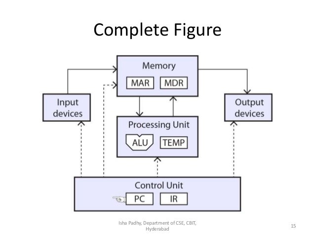
COMPUTER SYSTEM
cocMPUTER SYSTEM
Definition: Is a collection of entities(hardware,software and liveware) that are designed to receive, process, manage and present information in a meaningful format.
COMPONENTS OF COMPUTER SYSTEM
- Computer hardware - Are physical parts/ intangible parts of a computer. eg Input devices, output devices, central processing unit and storage devices
- Computer software - also known as programs or applications. They are classified into two classes namely - sytem software and application software
- Liveware - is the computer user. Also kwon as orgwareor the humanware. The user commands the computer system to execute on instructions.
a) COMPUTER HARDWARE
Hardware refers to the physical, tangible computer equipment and devices, which provide support for major functions such as input, processing (internal storage, computation and control), output, secondary storage (for data and programs), and communication.
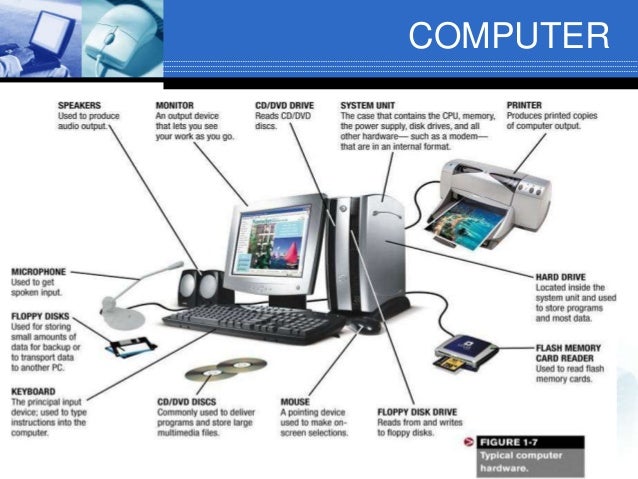
HARDWARE CATEGORIES (Functional Parts)
A computer system is a set of integrated devices that input, output, process, and store data and information. Computer systems are currently built around at least one digital processing device. There are five main hardware components in a computer system: Input, Processing, Storage, Output and Communication devices.

Components of a Computer
The internal architechtural design of computers may differ from one another. But there is a basic organization seen in all computers
The block diagram of basic computer organization is shown below:

The block diagram of basic computer organization is shown below:

The diagram shows that a computer consists of the Central Processing Unit (CPU), memory and input / output unit.
What is Arithmetic Logic Unit (ALU)? - Definition and meaning
Arithmetic Logic Unit (ALU): A subunit within a computer's central processing unit. ALU alu full form is Arithmetic Logic Unit , takes the data from Memory registers; ALU contains the logical circuit to perform mathematical operations like subtraction, addition, multiplication, division, logical operations and logical shifts on the values held in the processors registers or its accumulator.
It is the size of the word that the ALU can handle which, more than any other measure, determines the word-size of a processor: that is, a 32-bit processor is one with a 32-bit ALU.
After processing the instructions the result will store in Accumulator. Control unit generates control signals to ALU to perform specific operations. The accumulator is used as by default register for storing data. It is 16-bit register.
The simplest sort of ALU performs only addition, Boolean logic (including the NOT or complement operation) and shifts a word one bit to the right or left, all other arithmetic operations being synthesized from sequences of these primitive operations. For example, subtraction is performed as complement-add multiplication by a power of two by shifting, division by repeated subtraction. However, there is an increasing tendency in modern processors to implement extra arithmetic functions in hardware, such as dedicated multiplier or divider units.
The ALU might once have been considered the very core of the computer in the sense that it alone actually performed calculations. However, in modern SUPERSCALAR processor architectures this is no longer true, as there are typically several different ALUs in each of several separate integer and floating-point units. An ALU may be required to perform not only those calculations required by a user program but also many internal calculations required by the processor itself, for example to derive addresses for instructions that employ different ADDRESSING MODES, say by adding an offset to a base address. Once again, however, in modern architectures there is a tendency to distribute this work into a separate load/store unit.
The three fundamental attributes of an ALU are its operands and results, functional organization, and algorithms.
Operands and Results
The operands and results of the ALU are machine words of two kinds: arithmetic words, which represent numerical values in digital form, and logic words, which represent arbitrary sets of digitally encoded symbols. Arithmetic words consist of digit vectors (strings of digits).
Operator: Operator is arithmetic or logical operation that is performed on the operand given in instructions.
Flag: ALU uses many types of the flag during processing instructions. All these bits are stored in status or flag registers.
Functional Organization of an ALU
A typical ALU consists of three types of functional parts: storage registers, operations logic, and sequencing logic.
Arithmetic Logical Unit (ALU) Architecture
ALU is formed through the combinational circuit. The combinational circuit used logical gates like AND, OR, NOT, XOR for their construction. The combinational circuit does not have any memory element to store a previous data bit. Adders are the main part of the arithmetic logic unit to perform addition, subtraction by 2’s complement.
Control unit generates the selection signals for selecting the function performed by ALU.
Registers : Registers are a very important component in ALU to store instruction, intermediate data, output, and input.
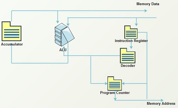
Logic Gates
Logic gates are building a block of ALU. Logic gates are constructed from diode, resistors or transistors. These gates are used in Integrated circuit represent binary input as ‘ON’ and ‘OFF’ state. Binary number 0 is represented by ‘OFF’ and Binary Number ’1’ is represented by ‘ON’ state in an integrated circuit.
OR gate : OR gate can take two or more inputs. The output of OR gate is always 1 if any of the inputs is 1 and 0 if all the inputs are false. OR gate performs an addition operation on all operand given in instructions. It can be expressed as X=A+B or X=A+B+C.
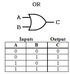
AND gate : AND gate takes two or more inputs. The output of AND gate is 1 if all inputs are 1. AND gate gives 0 results if any one of input in given data is 0. AND gate performs multiplication option on all inputs operands. It is represented by ‘.’ symbol. We can write it as- X=A.B or X=A.B.C.
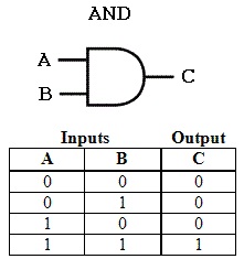
NOT gate : Not gate is used to reverse the result of gates or reverse Boolean state from 0 to 1 and 1 to 0.Not gate is also used with ‘AND’ and ‘OR’ gate. While using with AND or ‘OR’ gate, NOT gate is representing an as small circle in front of both gates. After using NOT gate, AND gates convert into NAND or ‘OR’ gate convert into NOR.
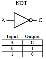
Registers: Registers provide fast memory access as a comparison to cache, RAM, hard disk. They are built on CPU. Register are small in size. Processing Intermediate data stored in registers.A number of registers used for specific purpose. ALU used four general purpose register. All these four registers are 16-bit register is divided into registers. 16-bit register implies that register can store maximum 16 bit of data.
Accumulator : Accumulator is 16 bit by default and general purpose register. By default means that any operand in instruction does not specify a particular register for holding the operand. That time operand will automatically store in AC. AC is used as two separate registers of 7 bit AL and AH. AC located inside the ALU. Intermediate data and result after execution will store in AC.AC used MBR to deal with memory.
Program Counter: PC stands for program counter. It is 16-bit register. It counts the number of instruction left for execution. It acts as a pointer for instructions and also known as Instruction pointer register. PC holds the address of next instruction to be executed. When an instruction is fetched from the register. Register get automatically incremented by one and point to the address of next instruction.
Flag register : it is also known as a Status register or Program Status register. Flag register holds the Boolean value of status word used by the process.
Auxiliary Flag : if two numbers are to be added such that if in the beginning of higher bit there is a carry. This is known as auxiliary bit.
Carry bit : Carry bit is indicate the most significant borrow or carry bit by subtracting a greater number than a smaller number or adding two numbers.
Sign Bit : Sign bit is a most significant bit in 2’s complement to show that result is negative or positive. It is also known as negative bit. If the final carry over here after the sum of last most significant bit is 1, it is dropped and the result is positive.
If there is no carry over here then 2’s complement will negative and negative bit set as 1.
Overflow bit : Overflow bit used to indicate that stack is overflow or not after processing the instruction. It is set to be 1 means that stack is overflow if it is 0 then its reverse to happen.
Parity Bit : Parity bit represent odd or even set of ’1’ bits in given string. It is used as error detecting code. Parity bit has two types: Even parity bit and an Odd parity bit.
In Even parity bit, we count the occurrence of I’s in the string. If a number of 1 bit is odd in counting than we will add even parity bit to make it even or if the number of 1 bit are even then even parity bit is 0.
Data Number of 1 bits even parity bit Data including Even Parity bit
1010111 5 1 11010111
Memory Address Register: Address register holds the address of memory where data is residing. CPU fetches the address from the register and access the location to acquire data. In the same way, MAR is used to write the data into memory.
Data Register: Data registers also Known as Memory Data Register. It holds the content or instruction fetched from memory location for reading and writing purpose. It is 16-bit register means that can store 216bytes of data. From Data, register instruction moves in Instruction register and data content moves to AC for manipulation.
Instruction register: Instruction holds the instruction to be executed .control unit of CPU fetch the instruction, decode it and execute the instruction by accessing appropriate content.IR is 16-bit register. It has two fields – Opcode and operand.
PC holds the address of the instruction to be executed. Once the address is fetched it gets incremented by 1.PC hold the address of next instructions. In this situation, IR holds the address of the current instruction.
Input /output register: Input register holds the input from input devices and output register hold the output that has to give to output devices.
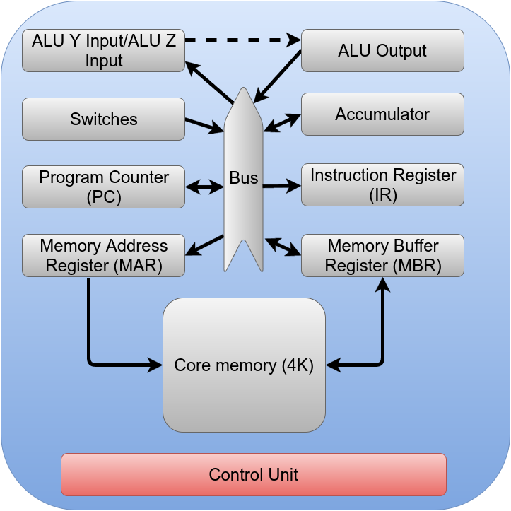
The control unit’s job is to read instructions from memory and then, based on those instructions, move data from one resource (for example, the memory) to another (for example, the accumulator). You’ll notice the dashed line between Y and Z and the ALU. That’s because Y and Z are actually the inputs to the ALU. The outputs include things like the sum of Y and Z, the inverse of Z, and so on.
The basic scheme for fetching instructions is this (Foster numbers from 1, so I will too):
- Fetch 1: Program counter (PC) to bus, load memory address register from bus, load ALU argument Z from bus, do memory read
- Fetch 2: Put constant 1 on the bus, load ALU argument Y from bus
- Fetch 3: Wait for memory access
- Fetch 4: Put Z+Y on the bus, load PC from bus
- Fetch 5: Load memory to memory buffer register
- Fetch 6: Put memory buffer register on bus, load instruction register
- Fetch 7: Available
- Fetch 8: Available
We omitted some details that don’t apply to modern systems. For example, part of the Fetch 5 cycle is to rewrite the data to Blue’s core memory. This is unnecessary for modern memory systems.
The Fetch cycle’s job is to read the instruction at the program counter and increase the program counter by 1. Fetch 1 is a good example of where the control unit does two writes in a single subcycle since the program counter has to go to the memory address register and Z.
For simple instructions, execution can occur in Fetch 7 and 8. Those instructions can fit in a single major cycle and don’t require an execute cycle. For example, a NOT instruction inverts the accumulator, so Fetch 6 for that instruction could put the accumulator on the internal bus and load Z. Then the final Fetch subcycle can move the ALU output to the accumulator. Also, it would have to flag the control unit to start a new Fetch cycle instead of an Execute cycle. In Blue’s original design, the STATE flag controls this and, by default, there is never an Execute cycle. So doing nothing, in the case of the NOT instruction, is sufficient to meet the requirement that the next cycle is a Fetch.
Some instructions need more work, however. In those cases, the Fetch 8 subcycle will set STATE to “E” (for execute). This provides 8 more subcycles for the control unit to manipulate resources in response to the instruction. This is especially important for instructions that access memory since you have to have another memory access cycle that doesn’t fetch an instruction. With modern high-speed memory, you might be able to condense everything into the 8 phases of Fetch, but remember Blue had relatively slow memory that needed a refresh after a read. The final step in any Execute cycle is to reset STATE to “F” so that the next cycle is a Fetch. Blue doesn’t need it, but in theory, STATE could be more than a bit if you had instructions that required multiple cycles (so you could have Execute 0, Execute 1, and so on).
How does the control unit know what to do? Each instruction has a 4-bit opcode (bits 15-12), and the remaining bits specify an address (now you see why Blue can only handle 4K words of memory). Once the instruction is in the instruction register, decoding the top 4 bits determines what happens in the next cycles.
IMPLEMENTATION
implement logic in Verilog or VHDL (although, you could draw gates like Foster did, using a simulation package, or maybe you want to build this in Minecraft). The concepts are the same however you do it.
You’d take all 16 instructions and build Fetch cycles for them (and Execute cycles for the ones you need). Then you can create logic to do each of the actions required. All of these that are the same get merged with an OR gate and fed to the register or other resource to make it do what it is supposed to do.
The resources are simple. You load the bus into a register, or you gate the register out to the bus. The ALU does simple logic internally, but otherwise is just a register that doesn’t just write its input back out. All the “smart” part is in the control unit.
Consider phase 4 of a Fetch cycle. It is supposed to have the ALU gate the sum output to the bus and then also have the PC read from the bus (this is how the CPU sets the next fetch address). In Foster’s design, this is a single AND gate. One input is the F bit (indicating a Fetch cycle), and the other is CP4 (meaning the 4th subcycle). The output fans out to both the ALU’s sum output gate and PC’s load input.
Presumably, other things will want to gate the sum output (the ADD instruction) or load the PC (a JMP instruction) so those outputs will really go to an OR gate that connects to the resource in question (see figure, below). For example, the sum output gate will also connect to an AND gate that merges the AND instruction decode with the inverse of F (indicating an Execute cycle), and CP8. The same output will drive the accumulator to read from the bus (again, through an OR gate that merges all the things that signal an accumulator load).

When you look at it this way, the CPU is simple. Just a bunch of readers and writers on a bus and a state machine that enables different items at different times. The resources are sometimes called the CPU’s datapath, and the resources are functional units.
OUT WITH THE OLD
We already mentioned the core memory features of Blue are hardly necessary today. There are a few other items you may have to (or want to) correct in Blue’s design. Fast memory allows you to optimize some of Blue’s cycles. In particular, you could read or write memory on each phase, if you wanted to. You could make the PC know how to increment itself so that the operation could share a slot with something that used the internal bus.
Probably the biggest change, though, is the clock generation. Foster uses a delay line to make the 8 phase clock. Modern designers don’t like to use delays like this for several reasons. First, component variations make it difficult to equalize short delays, especially across different machines. Second, components change with time and environmental factors, so delays like this would require careful design to be practical.
However, We think even Foster didn’t like that design. One of the exercise questions in the book challenges you to think of different ways to generate the clock. The most obvious, We think, to a modern designer is to make a clock at 8 times the require frequency and drive a 3-bit counter. Then decode the counter to 8 outputs. Alternately, you could use an 8-bit shift register and just cycle it on each clock pulse.
The I/O instructions are a bit dated. The instructions aren’t bad per se, as they just read or write from a device specified in the address field of the instruction (well, part of the field). However, the logic is set up for things like paper tape punches and readers. You’ll want to change that out. In my design, We simplified the I/O structure quite a bit.
Are devices used for entering data or instructions to the central processing unit. Are classifie according to the method they use to enter data.
a) KEYING DEVICES
Are devices used to enter data into the computer using a set of Keys eg Keyboard, key-to- storage and keypad.
i) The keyboard
Are devices used to enter data into the computer using a set of Keys eg Keyboard, key-to- storage and keypad.
i) The keyboard
Keyboard (similar to a typewriter) is the main input device of a computer . It contains three types of keys-- alphanumeric keys, special keys and function keys. Alphanumeric keys are used to type all alphabets, numbers and special symbols like $, %, @, A etc. Special keys such as <Shift>, <Ctrl>, <Alt>, <Home>, <Scroll Lock> etc. are used for special functions. Function keys such as <Fl>, <F2>, <F3> etc. are used to give special commands depending upon the software used e.g.F5 reloads a page of an internet browser. The function of each and every key can be well understood only after working on a PC. When any key is pressed, an electronic signal is produced. This signal is detected by a keyboard encoder that sends a binary code corresponding to the key pressed to the CPU. There are many types of keyboards but 101 keys keyboard is the most popular one.
How the keys are organized
The keys on your keyboard can be divided into several groups based on function:
- Typing (alphanumeric) keys. These keys include the same letter, number, punctuation, and symbol keys found on a traditional typewriter.
- Special (Control) keys. These keys are used alone or in combination with other keys to perform certain actions. The most frequently used control keys are CTRL, ALT, the Windows key, and ESC.
- Function keys. The function keys are used to perform specific tasks. They are labelled as F1, F2, F3, and so on, up to F12. The functionality of these keys differs from program to program.
- Cursor Movement (Navigation) keys. These keys are used for moving around in documents or WebPages and editing text. They include the arrow keys, HOME, END, PAGE UP, PAGE DOWN, DELETE, and INSERT and ARROW KEYS.
- Numeric keypad. The numeric keypad is handy for entering numbers quickly. The keys are grouped together in a block like a conventional calculator or adding machine.

B. POINTING DEVICESAre devices that enter data and instructions into the computer using a pointer that appears on the screen. The items to be entered are selected by either pointing to or clicking on them.e.g mice, joystick, touch sensitive screen, trackballs
i) THE MOUSE
A mouse is a small device used to point to and select items on your computer screen. Although mice come in many shapes, the typical mouse does look a bit like an actual mouse. It's small, oblong, and connected to the system unit by a long wire that resembles a tail and the connector which can either be PS/2 or USB. Some newer mice are wireless.
A mouse usually has two buttons: a primary button (usually the left button) and a secondary button. Many mice also have a wheel between the two buttons, which allows you to scroll smoothly through screens of information.
When you move the mouse with your hand, a pointer on your screen moves in the same direction. (The pointer's appearance might change depending on where it's positioned on your screen.) When you want to select an item, you point to the item and then click (press and release) the primary button. Pointing and clicking with your mouse is the main way to interact with your computer. There are several types of mice: Mechanical mouse, optical mouse, optical-mechanical mouse and laser mouse.
Basic parts
A mouse typically has two buttons: a primary button (usually the left button) and a secondary button (usually the right button). The primary button is the one you will use most often. Most mice also include a scroll wheel between the buttons to help you scroll through documents and WebPages more easily. On some mice, the scroll wheel can be pressed to act as a third button. Advanced mice might have additional buttons that can perform other functions.

Holding and moving the mouse
Holding and moving the mouse
Place your mouse beside your keyboard on a clean, smooth surface, such as a mouse pad. Hold the mouse gently with your index finger resting on the primary button and you thumb resting on the side. To move the mouse, slide it slowly in any direction. Don't twist it—keep the front of the mouse aimed away from you. As you move the mouse, a pointer (see picture) on your screen moves in the same direction. If you run out of room to move your mouse on your desk or mouse pad, just pick up the mouse and bring it back closer to you.
 Pointing to an object often reveals a descriptive message about it.The pointer can change depending on what you're pointing at. For example, when you point to a link in your web browser, the pointer changes from an arrow to a hand with a pointing finger .
Pointing to an object often reveals a descriptive message about it.The pointer can change depending on what you're pointing at. For example, when you point to a link in your web browser, the pointer changes from an arrow to a hand with a pointing finger .
Most mouse actions combine pointing with pressing one of the mouse buttons. There are four basic ways to use your mouse buttons: clicking, double-clicking, right-clicking, and dragging.
Clicking (single-clicking)
To click an item, point to the item on the screen, and then press and release the primary button (usually the left button).
Clicking is most often used to select (mark) an item or open a menu. This is sometimes called single-clicking or left-clicking.
Double-clicking
To double-click an item, point to the item on the screen, and then click twice quickly. If the two clicks are spaced too far apart, they might be interpreted as two individual clicks rather than as one double-click.
Double-clicking is most often used to open items on your desktop. For example, you can start a program or open a folder by double-clicking its icon on the desktop.
Right-clicking
To right-click an item, point to the item on the screen, and then press and release the secondary button (usually the right button).
Right-clicking an item usually displays a list of things you can do with the item. For example, when you right-click the Recycle Bin on your desktop, Windows displays a menu allowing you to open it, empty it, delete it, or see its properties. If you are unsure of what to do with something, right-click it.
C) SCANNING DEVICESAre devices that capture an object or a document directly from the source. They are classifie according to the technology used to capture data e.g. Scanners and Document readers.
i) ScannersUsed to capture a source document and converts it into an electronic form.
Example are - FlatBed and HandHeld scanners.


ii) Document readersAre documents that reads data directly from source document and convey them as input in the form of electronic signal. e
Types of Document Readers
i) Optical Mar Reader (OMR)
ii) Barcode readers

iii) Optical Character Readers
b) Magnetic Readers Reads data using magnetic ink.t uses principle of magnetism to sense data which have been written using magnetised ink.

THE CENTRAL PROCESSING UNIT ( C P U)Is the brain or the heart of a computer. Is also known as processor and consist of three units namely -
i) Control Unit ( C U)
ii) Arithmetic logic Unit ( A L U)
iii) Main Memory unit ( M M U)
 The system unit is the core of a computer system. Usually it's a rectangular box placed on or underneath your desk. Inside this box are many electronic components that process data. The most important of these components is the central processing unit (CPU), or microprocessor, which acts as the "brain" of your computer. Another component is random access memory (RAM), which temporarily stores information that the CPU uses while the computer is on. The information stored in RAM is erased when the computer is turned off.
i) ScannersUsed to capture a source document and converts it into an electronic form.
Example are - FlatBed and HandHeld scanners.
ii) Document readersAre documents that reads data directly from source document and convey them as input in the form of electronic signal. e
Types of Document Readers
i) Optical Mar Reader (OMR)
ii) Barcode readers
iii) Optical Character Readers
b) Magnetic Readers Reads data using magnetic ink.t uses principle of magnetism to sense data which have been written using magnetised ink.
THE CENTRAL PROCESSING UNIT ( C P U)Is the brain or the heart of a computer. Is also known as processor and consist of three units namely -
i) Control Unit ( C U)
ii) Arithmetic logic Unit ( A L U)
iii) Main Memory unit ( M M U)
The system unit is the core of a computer system. Usually it's a rectangular box placed on or underneath your desk. Inside this box are many electronic components that process data. The most important of these components is the central processing unit (CPU), or microprocessor, which acts as the "brain" of your computer. Another component is random access memory (RAM), which temporarily stores information that the CPU uses while the computer is on. The information stored in RAM is erased when the computer is turned off.
Almost every other part of your computer connects to the system unit using cables. The cables plug into specific ports (openings), typically on the back of the system unit. Hardware that is not part of the system unit is sometimes called a peripheral device. Peripheral devices can be external such as a mouse, keyboard, printer, monitor, external Zip drive or scanner or internal, such as a CD-ROM drive, CD-R drive or internal modem. Internal peripheral devices are often referred to as integrated peripherals. There are two types according to shape: tower and desktop.


Tower System Unit Desktop System Unit
Tower System Unit Desktop System Unit
A motherboard (mainboard, system board, planar board or logic board) is the main printed circuit board found in computers and other expandable systems. It holds many of the crucial electronic components of the system, such as the central processing unit (CPU) and memory, and provides connectors for other peripherals.

Motherboard
TYPES OF PROCESSORS
I) Comples Instruction Set Computers (CISC)
ii) Reduced Instruction Set Computers (RISC)
FUNCTIONS OF CENTRAL PROCESSING UNIT
- Process data
- Control sequence of operaions within the computers
- It gives command to all parts of a computer
- It control the use of the main memory in storing of data and instructions
- it provides temporary storage (RAM) and permanent storage(ROM) of data
THE CONTROL UNIT
Is the center of operations for the computer system, it directs the activities of the computer system.
Funlctions of Control Unit
In a computer's central processing unit (CPU), an accumulator is a register in which intermediate arithmetic and logic results are stored.
Without a register like an accumulator, it would be necessary to write the result of each calculation (addition, multiplication, shift, etc.) to main memory, perhaps only to be read right back again for use in the next operation. Access to main memory is slower than access to a register like the accumulator because the technology used for the large main memory is slower (but cheaper) than that used for a register. Early electronic computer systems were often split into two groups, those with accumulators and those without.
Modern computer systems often have multiple general purpose registers that operate as accumulators, and the term is no longer as common as it once was. However, a number of special-purpose processors still use a single accumulator for their work to simplify their design.
A given chip design is used for CPU's of many different speeds. The P2 and Celeron designs are named after Western US rivers: Deschutes, Klamath and Mendocino. More on this later.
In theory, a CPU is tested first at it's maximum speed. The ones that pass the testing process at this speed are marked as such and sold as top-of-the-line CPU's. Those that fail at the fastest speed are tested at successively lower and lower speeds until they run reliably. These slower cores are then marked with the speed at which they passed the testing process and sold as slower processors. At least, that's the theory. No one really knows how Intel decides which cores get marked for a given speed. Several other factors, such as customer demand and production quality, affect how many processors of each speed are produced.
A CPU of any given speed can usually be made to run somewhat faster if one is willing to play around with the motherboard settings. This is the overclocker's bread and butter. Now, through a convenient turn of events, Intel has produced a CPU with an unusually high capacity for overclocking.
Intel has long controlled the high-end CPU market while its competitors, Cyrix and AMD were gaining market share in the low- and mid-price range because of the popularity of lower priced PC's. Intel finally realized what was happening and wanted to recover the low ground while also keeping the high end market (can you say "total market domination"?). When Intel designed the CPU core for their newest line of processors, the P2, they changed the way the CPU was mounted. All P2's are mounted on a circuit board, called an SECC (Single Edge Contact Cartridge), that plugs into a special, patented CPU slot (Slot 1) similar to a PCI slot. [Intel calls the Celeron packaging a SEPP (Single Edge Processor Package) but it's still compatible with the Slot 1 connector, go figure.] AMD and Cyrix do not have a Slot 1 CPU, so if you want high-end speed, you need to buy an Intel processor. Thus the high-end market is preserved for Intel. Now, Intel needed a cheap Slot 1 CPU to corner the low-cost PC market.
Enter the Celeron line. To reduce production costs, Intel left out the expensive Level 2 cache. Also, to eliminate design costs, the original Celerons (C266 and C300) used the same CPU core as the new 350-450 MHz P2's (code name Deschutes). [Remember, design costs account for a huge percentage of the total cost of a CPU. Once in production, it costs exactly the same to manufacture a core destined for use as a 266 MHz processor as it does to use that same core in a 450 MHz processor.] Many media pundits immediately dubbed the Celeron a backward-stepping piece of crap because of the lack of the L2 cache. Later, perhaps due to the poor reviews from hardware critics, Intel released the Celeron 300A and 333 with 128 Kb of built-in cache. Again, they used basically the same core design with some modifications to incorporate the on-die cache. The C300A and the C333 modified Deschutes core carries the code name Mendocino. Since Celerons use a Slot 1 motherboard, you can't upgrade to one of Cyrix's or AMD's fast new CPU's later, when prices come down. They don't have Slot 1 CPU's and Intel has the patent. Now Intel has again regained a foothold in the below-$1000 PC market and insured that the upgrade dollars also come home to Papa Intel too.
Here's where it gets interesting. The fastest P2 CPU's (350 to 450) require a relatively new type of Slot 1 motherboard with the BX chipset. The BX motherboard runs at a bus speed of 100 MHz. They can also run at 66 MHz bus which allows them to accept slower P2 CPU's (233, 266, 300 and 333) and Celerons. The Celerons are supposed to be used on the earlier EX and LX generation of Slot 1 motherboards which run at 66 MHz only. Since the Celerons have the exact same core as the new architecture P2 CPU's, there's nothing to stop you from setting the bus to 100 MHz and running a Celeron at 400 or 450 MHz.
People started buying BX motherboards and Celerons and overclocking the hell out of them by setting the bus speed to 100 MHz. A chip meant to run at 266 running at 400 MHz and more was unheard of previously. It's all because Intel is trying to capture the low-cost CPU market without the R & D costs of a new chip. It's really a marketing stroke of genius when you think about it. Produce one type of CPU. Take the best ones, add 512 kb of fast, expensive cache and sell it as the top-of-the-line CPU for $700+. Take the rejects, leave off the expensive L2 cache and sell them as cheap Celerons. Except they're too smart for their own britches. The production yield of 450 MHz cores is too good and the "rejects" are too few and far between. Because they want to flood the market with $100 CPU's, they have to mark them as 266 to 333 MHz Celerons and sell them cheap anyway. It doesn't cost them any more since both chips came off the same production line. Because the P2-450 market is relatively small compared to the low- and mid priced market, the demand is greater for Celerons.
OPERATING SYSTEMS
- Is a software that acts as an interface between the user, application software and the computer hardware
EXAPMLE OF OPERATING SYSTEM
- Microsoft Disk operating system ( Ms DOS)
- Windows ( 98, 2000, XP, vista)
- Linux
- Unix
PARTS OF OPERATING SYSTEM
- Shell – it is the outer part of an operating system and it is responsible of interacting with the operating system
- Kernel – Responsible for managing and controlling computer resources such as the processor, main memory, storage devices, input devices, output devices and communication devices
RESOURCE UNER THE OPERATING SYSTEM CONTROL
- The processor
- Main memory
- Input/Output Device
- Secondary storage devices
- Communication devices and ports
FUNCTIONS OF OPERATING SYSTEM
- Job scheduling
– it is the process of the operating system to keep list of jobs currently being run by the computer and clocking them in and out of the processor.
- Interrupt handling
- It is a break from the normal sequential processing of instructions in a program
- Resource control and allocation
- It is situation where the processor gives a computer resources a unique number called interrupt number so that it can be able to recognize and prioritize it.
- Memory Management
- It is where the operating system constantly assigns main memory storage partitions to data an instructions
- Error handling
- It is a situation whereby an operating system alerts the user of errors that arises in ease of illegal operations, hardware or software failure.
- Input/output handling
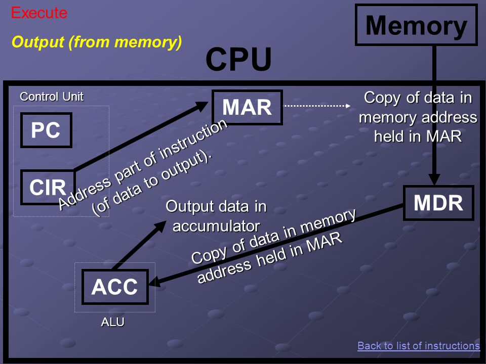
NOTE
What is interrupt request?
- Is a unique number that is given to a resource for identification purposes
What is the importance of interrupt computer
- To enable urgent tasks/ processes to b given the first priority during program execution
What is virtual memory
- Part of the hard disk that acts as maim memory
- Operating system organizes the main memory in blocks called page frames. The processes are divided into partitions that can fit in a page. The operatind system swaps these pages between the main memory and the hard disk. The part of the hard disk where these pages are held in the virtual memory.
What is a deadlock
- Is where a particular task holds a resourcs and refuses to release it for othe tasks to use.
CLASSIFICATION OF OPERATING SYSTEM
They are classified into three ways/types:-
- According to the number of tasks handled concurrently
- Single task – one task is operated at a any given time
- Multi-Task – More than one task is processed apparently simultaneously
- According to the number of users
- Single user – Single (One) user operates a computer at any given time
- Multi user – More than one user can operate the computer at the same time
- Human computer interface / G U I
- Interaction between the computer and the user.
- Command line – The user types the commands at the command prompt to activate them by pressing the enter key
Advantages
- Fast in operation by experienced users
- flexible
- Use Less memory
- Don’t require expensive hardware
Disadvantages
- Hard to learn and understand
- Not user friendly
- If you mistype or forgot the syntax of writing the command, you cannot operate it
- Difficult to learn
- Difficult to move information from one application to another
- Difficult to design and produce printed reports
- Do not support multi-users and multi-task
- Menu driven – The user is provided with a list of menu to choose from
Advantages
- More user friendly than command line
- More easier to learn and understand
- Eliminates the problem of forgetting the syntax of command since commands are provided for you
Disadvantages
- Slow to operate
- Not flexible
- Graphical User Interface(GUI) – The user interacts with the computer using icons and menus and select them using pointer
Advantages
- It is easy to learn and operate
- They make it easy to exchange information between application
- Reduce the user training time and cost due to their inform mode of operation
- It is more user friendly
- Supports multi user and multi task
Disadvantages
- Cost of GUI supporting hardware is higher
- Many objects on the GUI confuse new computer users
- - Require faster processors that are more expensive
WINDOW as used in operating system
Is a rectangular object created on a screen by operating system to contain input or output data for a particular program
PROPERTIES OF A WINDOW
- Title bar
- Display/ working area
- Horizontal and vertical scrolls bars
- Menu bars
- Status bar
- Tool bar
TYPES OF MENUS
- Pop up menu
- Pop down menu
- Sub menu( Cascading/ Side kick menu)
COMPUTER FILES
Are classifies into types :-
- System Files
Are files that contain information that is critical to the operations of the computer
- Application Files
Are files that holds programs or application files
INTERNET AND E-MAIL
THE INTERNET
The Internet links private PCs, public networks and business networks together using telephone lines to form one vast world-wide network.
It allows computer users to share and exchange information with each other wherever they are in the world.
The information on the Internet comes in many different formats.
These range from simple e-mail text files to music, video clips, computer software and even live television pictures.
The simplest way to connect to the Internet is to use a dial-up connection.
This type of connection requires a computer with a modem and access to a telephone line.
A modem converts a digital signal into an equivalent analogue signal that can be sent down a telephone line.
At the destination another modem is needed to convert the analogue signal back into a digital signal, which the receiving computer can understand.
The speed of a modem is measured in kilobits per second (Kbps) – this is a measure of how fast data can be transferred.
Dial-up modem connections offer data transfer speeds of up to 52 Kbps.
ISDN digital telephone lines offer a faster connection to the Internet.
ISDN connections offer data transfer speeds of up to 128 Kbps.
Dialup modems and ISDN lines are gradually being replaced by broadband connections that use a system called ADSL.
Broadband connections allow round-the-clock Internet access without having to dial a special telephone number and wait for a connection to be established.
ASDL is much faster than ISDN typically offering data transfer speeds of between 500 Kbps and 1,000 Kbps.
Some larger organisations use a leased line as their method of connection.
This is a private telephone line which is permanently open 24 hours a day.
An Internet Service Provider is a commercial organisation, which provides a connection to the Internet for other businesses or individuals.
Search engines allow users to surf the Internet for information by entering keywords.
Web addresses give the location of individual sites on the World Wide Web.
A web site can be quickly accessed using its address which is often referred to as a URL or Uniform Resource Locator.
A Uniform Resource Locator or URL gives the location of an individual site on the World Wide Web
Most URLs start with http//:www.
URLs often reveal the country of origin such as .uk for the United Kingdom.
URLs also indicate whether a site is commercial with either .co or .com for a commercial organisation, .gov for a government organisation and .ac for academic organisations.
Many businesses now have websites that allow Internet users to buy their goods or services online at any time of day or night throughout the year.
This type of online shopping also offers the advantages of not needing to travel anywhere or get pushed around in crowded shops.
Some companies do all of their business over the Internet and have no ordinary shops.
Advantages of online shopping:
money doesn’t have to be spent on normal business overheads like renting shops and paying employees;
customers can be offered a much wider choice of goods because they can be ordered from suppliers as required rather than having to be kept available on the shelves all the time;
money is not tied up in unsold stock or wasted on products that aren’t popular;
data about customers and their buying habits can be collected directly and used to offer a much more personalised service tailored to suit the needs of an individual customer.
Disadvantages of online shopping:
debit or credit card numbers can be intercepted by hackers during transmission and used to make unauthorised purchases;
criminals can set up fake web sites offering goods or services often using the name of a genuine company;
it is much easier for a business to gather information about its rivals by simply accessing their web sites — this can make it much harder to remain competitive.
Online booking systems allow Internet users to check the availability of and book things like:
theatre, cinema and concert tickets; seats on coaches, trains and aeroplanes; hotel rooms.
An online booking system is essentially a web site that can be used to access a remote database.

Dangers of the Internet:
hackers;
viruses;
undesirable material.
Hackers can be stopped using firewall software.
Viruses are often spread via e-mail and can be removed using virus checking programs.
Undesirable material can be blocked using special filtering software and adult supervision.

Advantages of the Internet:
easy communication with other people around the world;
valuable learning resource because Internet skills will be needed for jobs in the future;
enables more people to work from home;
a vast amount of information can be accessed;
up-to-date information can be accessed on-line without the need to await publication;
publishing documents on the Internet saves paper;
a valuable resource for companies to advertise and conduct business.
Disadvantages of the Internet:
much of the information isn’t checked and may be incorrect or irrelevant;
a large amount of undesirable material, such as pornography, is readily available;
messages sent across the Internet can be easily intercepted and are open to abuse by others;
large telephone bills can easily be run up;
too much time spent on the Internet could result in a lack of face-to-face interaction with others and a loss of social skills;
going on-line runs the risk of hackers or viruses being able to damage your computer.
WORD PROCESSORS
WORD PROCESSORS
Is an application software that enables the user to create, save, edit,format and print a document.
Example of word processors
- Microsoft Word
- Word star
- Word perfect
- Corel
- Lotus
- Word pro
- K Word
- Abiword
- PC-Write
Advantages of using a word processor over a manual type writer
- A document can be stored in a computer for future reference
- Have special editing tools eg spelling and grammar checkers
- One can easily insert or replace a word or phrase without affecting the neatness of a document
- One can easily produce many copies using a printer without retyping
Features of a word processors
- A word wrap which automatically starts a new line if there is insufficient room at the hand margin
- Availability of different fonts, character sizes and styles
- Text paragraph and page formatting eg text alignment, indenting, page number etc
- Search and replace command which allow replacement of every incidence of a certain combination of characters with a set of characters
- Undo which allows action that have been performed to be reversed
- Printing of documents single or multiple choices
- Mail merging that is very essential while similar letters have to be sent
- Ability to create and import tables, text and graphics from other programs
Factors to consider when selecting a word processor
- The type of operating system installed
- Its user friendliness
- Its formatting and editing features
- Whether it is commercial or open source software
Parts of a Microsoft word window
1. Title bar
It a bar at the top of a the window and it displays the titile currently running application at task
2. Menu Bar
2. Menu Bar
It contains menus that provides lists of commands
3. Status bar
It is an interactive strip at the bottom of the screen that acts as a communication link between the user and the program.

Editing – Its is making necessary changes in a document
TWO TYPING MODES
Insert Mode – When text is typed between the existing words or characters it pushes the existing text forward without replacing them
Type over mode – When text is typed between words or characters the new text automatically replaces the existing text by deleting it.
Formatting - Applying various styles or features in order to enhance the document appearance
Text Formatting Features
- Changing font type, size style
- Changing font colour
- Underlining – Placing a line at the bottom of a text
- Bolding – Making the text appear more darker than the rest
- Italicizing –making the text slant forward
- Superscript and subscript
- Strikethrough
DATA PROCESSING CYCLE
Data procesing refers to the transformating raw data into meaningful output.
Data can be done manually using a pen and paper, mechanically using simple devices eg typewritter or electronically using modern dat processing toolseg computers
Stages of the data processing cycle.
Data can be done manually using a pen and paper, mechanically using simple devices eg typewritter or electronically using modern dat processing toolseg computers
Stages of the data processing cycle.
Data collection involves getting the data/facts needed for processing from the point of its origin to the computer
Data Input- the collected data is converted into machine-readable form by an input device, and send into the machine.
Processing is the transformation of the input data to a more meaningful form (information) in the CPU
Output is the production of the required information, which may be input in future.
The difference between data collection and data capture.
Data capture is the process of obtaining data in a computer-sensible form for at the point of origin (the source document itself is prepared in a machine-sensible form for input)
Data collection involves getting the original data to the ‘processing centre’, transcribing it, converting it from one medium to another, and finally getting it into the computer.
The 5 stages of data collection.
Data creation
Data transmission
Data preparation
Media conversion (i.e, conversion of data from one medium to another
Input validation
Sorting
Relevance of the term garbage in garbage out (GIGO) in reference to errors in data processing.
The accuracy of the data entered in the computer directly determines the accuracy of the information given out.
Give and explain two transcription and two computational errors committed during data processing.
Misreading errors: -they occur when the user reads source document incorrectly, thus entering wrong values, e.g. a user may confuse 5 in the number 586 with S, and type S86 instead.
Transposition errors: - they result from incorrect arrangement of characters (i.e., putting characters in the wrong order especially when keying data onto a diskette), e.g. the user may enter 396 instead of 369 computational errors
Overflow errors: -An overflow occurs if the result from a calculation is too large to fit in the allocated memory space, e.g., if the allocated memory space is able to store an 8-bit character, then an overflow will occur if the result of the calculation gives a 9-bit number.
- Underflow
- Truncation: 0.784969 784
- Rounding error:30.6666 7
- Algorithm or ,logical errors
Data integrity.
Data integrity refers to the dependability, timeliness, availability, relevance, accuracy & completeness of data/information
Ways of minimizing threats to data integrity.
- Backing up the data on external storage media
- Enforcing security measures to control access to data
- Using error detection & correction software when transmitting data
- Designing user interfaces that minimize chances of invalid data being entered.
Briefly explain real-time processing.
- Airline reservation systems
- Theatre (cinema) booking
- Hotel reservations
- Banking systems
- Police enquiry systems
- Chemical processing plants
- Hospitals to monitor the progress of a patient
- Missile control systems
Advantages and disadvantages of
Real-time system.
Advantages
- Provides up-to-date information
- The information is readily available for instant decision-making
- Provides better services to users/customers.
- Fast &reliable
- Reduces circulation of hardcopies.
Disadvantages
- Require complex Os & are very expensive
- Not easy to develop
- Real time systems usually use 2 or more processors to share the workloads, which is expensive.
- Require large communication equipment.
The Differentiate between CPU bound jobs and I/O bound jobs.
CPU bound jobs require more of the CPU time to process these jobs. Most of the work the I/O devices perform is on the Input; and Output; hence, they require very little CPU time.
Most companies are now shifting from the use of geographically distributed personal computers. This method of data processing is known as Distributed Data Processing (DDP)
Three computing resources that can be distributed.
-CPU (Processors) time
-Files
-Application software
-Data/information/messages
-Computer processing power
-Memory (computer storage)
- Input/Output devices, e.g. printers
-communication devices/communication port
Examples of industries and business organizations that extensively use distributed processing systems.
- Banks
- Computerized retails stores, e.g. supermarkets
- Learning institutions with many departmental offices
- Bureaus or communication cyber cafes
- Airline reservation systems
Benefits and three risks that might be associated with the distributed data Processing system.
The load on the host computer is greatly reduced
- The use of low cost minicomputers minimizes the cost in data processing
- Delays in data processing are reduced
- Provides better services to the customers
- There is less risk in case of system breakdown
- The design & implementation of the system is less complex due to decentralization
- The level of expertise required is less.
Risks
- Data duplication is very common
- Programming problems occur with microcomputers & minicomputers
- Security threats, i.e. the data & information sent one the network from one place to
- another can be tapped, or listened to by unauthorized parties
- More training is needed for the users involved
- It is expensive due to the extra cost of communication equipment.
The concept of multi-programming
A Multi-programming system allows the user to run 2 or more programs, all of which are in the computer’s main memory, at the same time.
Benefits that are derived from multi-programming
- It increases productivity of a computer
- Reduces the CPU’s idle time
- Reduces the incidence of peripheral bound operation
Advantages of storing data in computer files over the manual filing system
- Stored information takes up less space
- Easier to update and modify
- Provides faster access and retrieval of data
- Reduces duplication of data or stored records
- Cheaper
- Enhances data integrity (i.e. accuracy and completeness)
The difference between logical and physical computer files.
A logical file is viewed in terms of what data items it contains and what processing operations may be performed on the data
A physical file is viewed in terms of how the data items found in a file are arranged on the storage media and how they can be processed.
Arrange the following components of the information system data hierarchy in ascending order of complexity:
Field, Database, Byte, Record, Bit, and file
Bit Byte Field Record File Database
Types of computer processing files
i) Report file- It contains a set of relatively permanent records extracted from the data in a master file.
They are used to prepare reports, which can ve printed at a later date, e.g. report on student’s class performance in the term, extract of students who have not cleared their school fees, report on absentees
ii) Backup file- Used to backup data or to hold duplicate copies of data/information from the computer’s fixed storage or main file for security purposes e.g. a copy of all the students admitted in a school fees, report on absentees
ii) Backup file- Used to backup data or to hold duplicate copies of data/information from the computer’s fixed storage or main file for security purposes e.g. a copy of all the students admitted in a school fees, report on absentees
iii) Reference file - Used for reference purposes. It contains records that are fairly permanent or semi-permanent, e.g. Deductions in caution money, wage rates, tax deductions, employees address, price lists etc.
iv) Sort file – used to sort/rank data according to a given order, e.g. ranking position in a class of students.v) Transaction file - Is used to hold input data during transaction processing. It is later used to update master files and audits daily, weekly or monthly transaction.
FILE ORGANISATION METHODS
What is file organization?
- It is the way records are arranged (laid out) within a particular file or any secondary storage device in a computer
- Refers to the way data is stored in a file
- File organization is important because it determines the method of access, efficiency, flexibility and storage devices to be used.
Methods of file organizatioSequential and serial
In sequential file organization, records are stored in a sorted order using a
key field, while in serial; the records are stored in the order they come into the file, and are not sorted in any way.
Random and indexed-sequential
Random and indexed-sequential
In random file organization, records are stored in the file randomly and accessed directly, while in indexed –sequential, the records are stored sequentially but accessed directly using an index.
Serial file organization
Records are in a file are stored and accessed one after another on a storage medium
Indexed sequencial file organization method
Indexed sequencial file organization method
Similar to sequential method, only that an index is used to enable the computer to locate individual records on the storage media.
ELECTRONIC DATA PROCESSING MODES
DATA PRESENTATION IN A COMPUTER
Description
Computers are classified according to Functionality, physical size and purpose.
According to functionality, computers can be analog, digital or hybrid.
Digital computers produce data that is in discrete form, analog computers process data in that is in continuous in nature while hybrid computers process both discrete and continuous data.
In digital computers , the user input is first converted and transmitted as eklecrical pulses that can be represented by two distinct states ONE and OFF.
Analog and Digital Signal
Graphically they look different in their appearance, they repeat themselves at equal time interval. The electrical signal or waveform of this nature are said to be periodic. A periodic wave representing a signal is described using THREE PARAMETERS
Amplitude (A)
Frequency (f)
Periodic Time (T)
Amplitudes (A)
This is the maximum displacement that the waveform of electrical signal can attain.
Eg
Frequency (f)
This is the number of circles made by the signal in one second.
It is measures in units called hertz (hz) which is equivalent to 1 cycle / second.
Periodic time (T)
The time taken by the signal to complete one cycle and is given by the formula T = I/F, where f is the frequency of the wave.
When a digital signal is sent over an analog telephone line eg E-mail, it has to be converted to analog signal. This is done by connecting a device called MODEM (Modulator/Demodulator) to the computer.
Role of MODEM
A MODEM converts (modules) data from digital to analogue form to be transmitted
over the telephone ling. At the receiving end, the modem attached to the
receiving computer converts (demodulates)the analogue signal back to the original digital form.
Reasons for using binary in digital technology.
- It is easier to develop devices that understand binary language
- Devices designed using binary logic are simple, more reliable & consume less
energy.
Terminogies as used in data representation.
i) Bit - The smallest binary unit, ‘0’ or ‘1ii) Byte - A group/collection of 8 bits used to represent a character.
iii) Nibble - a group of four binary digits usually representing a numeric
value
iv) word - The total number of bits that a single register of a particular
iv) word - The total number of bits that a single register of a particular
machine can hold
TYPES OF DATA PRESENTATION
Is the better way of handling complex types of data ( long streams of binary digits). Higher number systems are used in computing to reduce the streams of binary into manageable form, thus helps to improve the processing speed and optimize memeory usage.
CATEGORIES OF NUMBERS SYSYTEM
- Decimal Number system
- Binary Number system
- Octal Number system
- Hexadecimal Number system
DECIMAL NUMBER SYSTEM
Decimal ( deci) means ten
Has ten digits ranging from 0 – 9 because the system has ten digit.
Also called base ten or denary number system and written with subscript 10 i.e x 10
BINARY NUMBER SYSTEM
Uses two digits namely 1 and 0
The place values increases by factors of two
Written as base two i.e x 2
Consider a binary number such as 100112, the right most digit has a place value of 2 x 10 while the left most has a place value of 2 x 13
Place Value (2 n)
|
Eights 23 = 8
|
Four 22 = 4
|
Twos 21 = 2
|
Ones 20 = 1
|
Binary digit
|
1
|
0
|
1
|
1
|
OCTAL NUMBER SYSTEM
Uses eight bits running from 0 – 7
The place value go up in factors of eight from right to left
Example. – 72458
Place Value (8 n)
|
83 = 512
|
82 = 64
|
81 = 8
|
80 = 1
|
Binary digit
|
7
|
2
|
4
|
5
|
NB
The decimal equivalent of 72458 is
The decimal equivalent of 72458 is
N10 = (7x83) + (2x82) + (4x81) + (5x80)
= (7x512) + (2x64) + (4x8) + (5x1)
= 3584 + 128 + 32 + 5
= 374910
HEXADECIMAL NUMBER SYSTEM
It is radix of sixteen (16)
Uses 16 digits ranging from 0 – 9 and letters A to F. A is equivalent to 10 while F is equivalent to 15.
The place value goes up in factors of sixteen (16) from right to left
Example 1
Convert 11116 to Decimal equivalent
Solution
162 = 256
|
161 = 16
|
160 = 1
|
1
|
1
|
1
|
Example 2
Convert A916 to its decimal equivalent
Solution
161 = 16
|
160 = 1
|
A
|
9
|
A = 10 - 10 x 161 = 160
1 = 1 - 1 x 160 = 9
Ad the two – 160 + 9 = 169
Therefore A916 = 16910
Uses of hexadecimal notation in a computer.
Helps to manage long binary digit properly
Helps to improve the processing speed and optimize memory usage.
BINARY ARITHMETIC OPERATION
Representation of signed binary numbers
Ways of representing binary number (positive) or (negative)
- Prefixing an extra sign bit to binary
- Using ones complement
- using two complement
Prefixing an extra sign bit to a binary number
A signed number has a prefix + for positive number and represented by prefixing a digit
0 and a negative number represented by prefixing a digit 1
USING COMPLEMENT
One’s compliment to solve the following the following sum: - 510
2
|
5
|
Rem
|
2
|
2
|
1
|
2
|
1
|
0
|
1
|
1
|
Perform the following Binary arithmetic:
11100111 + 00101110
11100111
00101110 +
(1) 00010101 =1000101012
XO___XO ++DW DW SAW A small portion of ADA on individual computer systems before we connect ADA computer network communication to the proxy system and networking firewall

The Microprocessor
The term microprocessor typically refers to the central processing unit (CPU) of a microcomputer, containing the arithmetic logic unit (ALU) and the control units. It is typically implemented on a single LSI chip. This separates the "brains" of the operation from the other units of the computer.

The CPU as a Logisim Circuit
If you now unpack the Zip file at the top of this page, you will find the CPU as a Logisim circuit. When you load it into Logisim, you need to do three things:
- Load the control ROM with an image.
- Load the decision ROM with an image.
- Load the RAM with a program image to run.
The output from my microassembler below is two ROM images, ucontrol.rom and udecision.rom, which you can load into the simulated CPU ROMs in the ucodelogic component. The output from my assembler below is a RAM image (ending with the suffix .ram) which you can load into the simulated CPU RAM in the main circuit.
If you reset the simulation in Logisim, the ROMs are kept intact but the RAM is wiped, so you need to reload it. Of course, if you make any changes to the microcode with the microassembler, you need to reload the ROM images, too.
An example of microprocessor architecture.
The microprocessor contains the arithmetic logic unit (ALU) and the control unit for a microcomputer. It is connected to memory and I/O by buses which carry information between the units.
Microcomputer Example
Typical microcomputers employ a microprocessor unit (MPU), a clock, and interfaces to memory and external input/output devices. The units are connected by buses which transfer information between them.

Buses: The exchange of information.
Information is transferred between units of the microcomputer by collections of conductors called buses.
There will be one conductor for each bit of information to be passed, e.g., 16 lines for a 16 bit address bus. There will be address, control, and data buses.

Arithmetic Logic Unit
All the arithmetic operations of a microprocessor take place in the arithmetic logic unit (ALU). Using a combination of gates and flip-flops, numbers can be added in less than a microsecond, even in small personal computers. The operation to be performed is specified by signals from the control unit. The data upon which operations are performed can come from memory or an external input. The data may be combined in some way with the contents of the accumulator and the results are typically placed in the accumulator. From there they may be transferred to memory or to an output unit.

The Accumulator
The accumulator is the principal register of the arithmetic logic unit of a microprocessor. Registers are sets of flip-flops which can hold data. The accumulator typically holds the first piece of data for a calculation. If a number from memory is added to that date, the sum replaces the original data in the accumulator. It is the repository for successive results of arithmetic operations, which may then be transferred to memory, to an output device, etc.
We describes the components within the architecture of a Central Processing Unit (CPU). We will illustrate the operations performed by the CPU, and examine computer memory, considering the various types of memory found within a computer.
A PC passes data between the CPU, internal memory, and Input/Output controller (I/O) via a data highway called a bus.

Several types of buses transmit power, data, address and control signals. Collectively these are known as system buses.
System buses are classified by their data bandwidth (8 bit, 16 bit, 32 bit...). A higher data width increases the speed transfer of data.
| The Von Neumann architecture is based on a single computing element, the Central Processing Unit (CPU). | |
 The top of a 486 CPU processor chip |  chip showing pins |
| Processor chips vary slightly in look depending on which company has made them. They are all made up from the same elements except some work faster and more efficiently than others. The above examples are Intel® processor chips, a popular brand. | |
The CPU architecture executes instructions one after another. It consists of a single control unit, an arithmetic logic unit (ALU), and registers.
The CPU is responsible for acting as the 'brain' of the computer.
The function of the CPU is to execute programs stored in the main memory by fetching instructions, examining them, and executing them one after the other.

Tasks carried out by a CPU are listed below:
- decoding the instructions within a computer
- sequencing the reading and writing of data within the CPU and externally on the data bus
- controlling the sequence in which instructions are executed
- controlling the operations performed by the ALU

The arithmetic logical unit (ALU) is responsible for performing arithmetic and logical operations and comparisons of data.

The CPU also contains a small high speed memory which is used to store temporary results and control information.
This memory consists of a number of registers, each performing a specific function.

- Accumulators - serve the purpose of holding data used in calculations.
- Address Registers - are used for storing the memory location of data or instructions to be used by a program.
- Stack Pointer - this register is used during sub-routine nesting and stack based arithmetic.
- Status Register - this register provides a service to the CPU by maintaining the status of the last operation carried out by the ALU.
- Instruction Pointer - sometimes referred to as the program counter, the pointer is responsible for retaining the memory address of the next instruction to be executed.
The following pages illustrate the operations performed within a computer during a fetch and execute cycle.
The control bus performs a read operation:

The control unit in the CPU prompts memory to put the instruction onto the data bus enabling the CPU to read the instruction onto its instruction decoder which is part of the control unit:

The next step involves the CPU decoding the instruction.
This instruction is then executed. For example, if the instruction is for the Control Unit to load the contents of the memory location 112 into the accumulator:


The control unit sets the address bus to location 112 and puts the value of the accumulator onto the data bus.
Finally the control bus performs a memory write operation:
Finally the control bus performs a memory write operation:

Control Unit of Microprocessor
The control unit of a microprocessor directs the operation of the other units by providing timing and control signals. It is the function of the microcomputer to execute programs which are stored in memory in the form of instructions and data. The control unit contains the necessary logic to interpret instructions and to generate the signals necessary for the execution of those instructions. The descriptive words "fetch" and "execute" are used to describe the actions of the control unit. It fetches an instruction by sending and address and a read command to the memory unit. The instruction at that memory address is transferred to the control unit for decoding. It then generates the necessary signals to execute the instruction.
Buses
The term bus, in computer language, refers to a system within the computer hardware that moves data. Without buses, the computer may do calculations, but lacks the ability to move the resulting data to any form of output device. Buses fall into several categories and types. The computer bus is sometimes referred to as the address, local, or data bus. The bus is also sometimes called the Peripheral Component Interconnect.

A bus allows the various devices both inside and attached to the system unit to communicate with each other. Word size is the number of bits the processor can interpret and execute at a given time.
Data bus
The data bus acts as a conduit for data from the keyboard, memory and other devices. It passes information at speeds up to billions of characters per second. The central processor reads the data, performs calculations, and moves new data back to memory, the hard drive and other locations. The control bus determines which direction the data is moving.
Address bus
The computer must be able to access every character of memory rapidly, so every character has its own address number. The central processor specifies which addresses it wants to read or write and the address bus carries this information to a memory controller circuit, which locates and fetches the information. Some locations, called random-access memory, hold program instructions and temporary calculation results. Other locations point to the hard drive, mouse and keyboard. The control bus specifies which of these two sets of addresses become active for a particular memory operation.
Internal Computer Bus
Data movement between devices internal to the computer occur through the internal bus. This function includes transferring information between such devices as the video card, the random access memory or the hard disk.
External Computer Bus
Data movement outside the computer occurs through the external bus. This can include devices such as Small Computer System Interfaces (SCSI), printers or even monitors.
The types of expansion buses on a motherboard determine the types of cards you can add to a computer.
Types of expansion buses :
- An ISA (Industry Standard Architecture) bus, the most common and slowest expansion bus, connects to devices such as a mouse, modem card, sound card, and low-speed network card
- A local bus is a high-speed expansion bus used to connect higher speed devices such as hard disks
- An Accelerated Graphics Port (AGP) is a bus designed by Intel to improve the speed with which 3-D graphics and video transmit
- The universal serial bus (USB) and 1394 bus are buses that eliminate the need to install expansion cards into expansion slots
- A PC Card bus is the expansion bus for a PC Card
Cache
A special high-speed storage mechanism. It can be either a reserved section of main memory or an independent high-speed storage device.
Two types of caching are commonly used in personal computers: Memory caching and Disk caching.
Memory cache
Sometimes called a cache store or RAM cache, is a portion of memory made of high-speed static RAM (SRAM) instead of the slower and cheaper dynamic RAM (DRAM) used for main memory.
A memory caching is effective because most programs access the same data or instructions over and over. By keeping as much of this information as possible in SRAM, the computer avoids accessing the slower DRAM.
Disk caching
Disk caching works under the same principle as memory caching, but instead of using high-speed SRAM, a disk cache uses conventional main memory. Disk caching works under the same principle as memory caching, but instead of using high-speed SRAM, a disk cache uses conventional main memory.

Ports
A port is the point at which a peripheral attaches to or communicates with a system unit (sometimes referred to as a jack).
Parallel and Serial Ports
When "computer ports" are discussed, the type most often referred to are hardware ports, which allow information from outside sources to enter the computer. Hardware ports can be parallel or serial, among other varieties. The rarer serial port transmits one bit of data at a time, while the more common parallel port simultaneously transmits multiple bits across multiple wires. Examples of other hardware ports include USB, Ethernet, Firewire and HDMI, all of which are parallel ports.
USB port
USB ports allow connections between USB-powered devices and a computer or another electronic device, such as a printer. USB ports have a data transfer rate of over 400 megabytes per second (Mbps).
Video and Audio Ports
All computers have several different ports on their exterior that export or import video and audio feeds. Your computer's headphone jack is one example of an audio port. You must connect a monitor's display cable to your computer's graphics port to use a laptop with an external monitor. HDMI ports are used to connect high definition (HD) monitors. These ports make it possible for multimedia computers to interact with video and audio equipment.
Bays Citing
Bay is an opening inside the system unit which you can install additional equipment.
Drive bay - refers to a site in personal computers where a hard or floppy disk drive, CD-ROM drive or tape drive can be installed. Plus the number of drive bays in a computer determines how many mass storage devices can be internally installed.

PC Connected

Unbelievable but true, you can connect your old Aquarius to your PC, and send data to the PC.
You will need :-
- 1 x 9 Pin-D Female connector
- 1 x 1/4 Inch stereo audio connector jack.
- 1 piece of 3 conductor wire.
Audio Jack TIP ---> Pin 2 (RxD) of the 9 pin D
Audio Jack RING ---> pin 4 (DTR) of the 9 Pin D
Audio Jack SLEEVE ---> pin 5 (GND) of the 9 pin D
Connect pins 7 (CTS) and 8 (RTS) of the 9 Pin D together.
Connect pins 4 and 6 of the 9 pin D together
Audio Jack RING ---> pin 4 (DTR) of the 9 Pin D
Audio Jack SLEEVE ---> pin 5 (GND) of the 9 pin D
Connect pins 7 (CTS) and 8 (RTS) of the 9 Pin D together.
Connect pins 4 and 6 of the 9 pin D together
Push the audio jack into the PRINTER port of the Aquarius and the 9 Pin D into the serial port of your PC.
Using your favorite comms package such as HyperTerminal or PuTTY, set the comms parameters to 1200 baud, no parity, 8 data bits, 1 stop bit and Hardware Handshaking. You must enable hardware handshaking as this provides the 'printer ready' signal to the Aquarius.
Anything you LPRINT or COPY from the Aquarius will be received by the PC .
The hand controllers
The hand controllers are controlled by the IO-Ports A and B of the AY-3-8910 Programmable Sound Generator (PSG). In order to read the hand controllers you should have some knowledge about how the PSG works. Please make sure you have read the pages about programming the AY-3-8910.
| switch | Data bus grounded | Hex code | Decimal code |  |
|---|---|---|---|---|
| k1 | D6 | BF | 191 | |
| k2 | D7,2 | 7B | 123 | |
| k3 | D7,5 | 5F | 95 | |
| k4 | D5 | DF | 223 | |
| k5 | D7,1 | 7D | 125 | |
| k6 | D7,0 | 7E | 126 | |
| P1 | D1 | FD | 253 | |
| P2 | D1,4 | ED | 237 | |
| P3 | D1,0,4 | EC | 236 | |
| P4 | D1,0 | FC | 252 | |
| P5 | D0 | FE | 254 | |
| P6 | D0,4 | EE | 238 | |
| P7 | D3,0,4 | E6 | 230 | |
| P8 | D3,0 | F6 | 246 | |
| P9 | D3 | F7 | 247 | |
| P10 | D3,4 | E7 | 231 | |
| P11 | D3,2,4 | E3 | 227 | |
| P12 | D3,2 | F3 | 243 | |
| P13 | D2 | FB | 251 | |
| P14 | D2,4 | EB | 235 | |
| P15 | D1,2,4 | E9 | 233 | |
| P16 | D1,2 | F9 | 249 |
Note on double keying
If any two switches (keypad and disc) of the hand controller are pressed at the same time, a unique code will be generated exept the following switch combinations:
If any two switches (keypad and disc) of the hand controller are pressed at the same time, a unique code will be generated exept the following switch combinations:
| Switch combinations generating the same code | Code | Data Bus Grounded | |
|---|---|---|---|
| (I) | P5 K5 | 124 | D0,1,7 |
| P4 K5 | |||
| K6 K5 | |||
| K6 P1 | |||
| K6 P4 | |||
| (II) | P5 K2 | 122 | D0,2,7 |
| K6 K2 | |||
| K6 P13 | |||
| (III) | K5 P16 | 121 | D1,2,7 |
| K5 P13 | |||
| K5 K2 | |||
| P1 K2 | |||
| P16 K2 | |||
| (IV) | K6 P16 | 120 | D0,1,2,7 |
| K2 P4 | |||
| (V) | K3 | 95 | D7,5 |
| K3 K4 | |||
Do not use the above codes whenever possible.
In order to read the hand controller you first have to set bits 6 and 7 of R7 to 0. After you have set the two bits to zero, all you have to do to read the hand controllers is to output the correct value (register) to port 247, and then read the input from port 246.
OUT 247, 14 ; for the right-hand controller
OUT 247, 15 ; for the left-hand controller
A small machine code routine to read the right-hand controller for the Aquarius looks like:
data    label   opcode  operand    comment
 62,  7    start:  LD     A, 7       ; Select register 7
211,247     OUT    (247),A    ; Send to the register pointer
 62, 63     LD     A, 63      ; Value for register
211,246     OUT    (246),A    ; Send to data transfer
 62, 14     LD     A, 14      ; Select register 14
211,247     OUT    (247),A    ; Send to the register pointer
219,246     IN     A, (246)   ; Read the value for R 14
 50,216,57    LD     (14808),A  ; Store value at mem location 14808
201     RET        ; Return to basic
Which results in the following BASIC prog:
5 ?CHR$(11)
10 DATA 62,7,211,247,62,63,211,246,62,14,211,247,219,246,50,216,57,201
20 I=14790:POKE14340,198:POKE14341,57
30 READX:POKEI,X:I=I+1:IFX<>201THEN30
40 X=USR(0)
50 ?PEEK(i)
60 IFINKEY$=""THEN40
You should change the number 14 in the DATA line into 15 to read the left-hand controller.
After the machine code we use the PEEK command to read the value at memory location 14808 and use the print command to show it on screen. The program loops until a key is pressed on the keyboard.
I've choosen memory address 14790 as the start address for the machine code. This is -almost- directly after the BASIC program. The value returned by the hand-controller is stored at memory address 14808 which in turn is directly after the machine code.
If you want to use this routine in your own BASIC program then you'll have to modify the start address of the machine code at a higher memory address and also the value returned by the hand-controller must be stored at a higher location.
The tight numbers have been choosen so the program still works on a standard Mattel Aquarius computer without memory upgrade.

RAM Guide
DRAM chips
Now that we know how to read from and write to a simple SRAM chip, let's look at the more common DRAM chip and see how to use it. DRAM, as I've mentioned earlier, is more complicated than SRAM because the charges placed on its memory cells leak out over time. (One of my EE professors used to say, "the difference between SRAM and DRAM is that SRAM works and DRAM doesn't.") So most of DRAM's peculiar and complicated characteristics arise from the fact we're trying to take memory that actually doesn't work and make it work.
But before we talk more about the "making it actually work" aspects of DRAM, let's look at a simple DRAM chip and discuss the pin-outs.
One of the earliest, simplest, and most important DRAM chips was the 2118, introduced by Intel in 1979. The 2118 was a 16K x 1 DRAM packaged in an 18-pin DIP. That "16K x 1" part means that it had 16384 cells and it read or wrote 1 data bit at a time. (I couldn't find an online datasheet for the 2118, so I did some Paintshop Pro mojo on the above diagram to get the following one, which I based off a printed 2118 pin-out that I have.)

Looking at the above diagram, you'll probably notice a few immediate differences from the earlier SRAM module. The primary difference, and the one from which all the others stem, is that the number of address lines is cut in half. So you're probably wondering, if this 16K DRAM has half the number of address lines as the 16K SRAM, then how does it address all 16K memory cells? The answer is simple, but it makes interfacing with the DRAM more complicated: the address is cut into halves, and the two halves are applied to the address pins on two separate clock cycles. So the 14-bit address would be split into two, 7-bit chunks, and the two chunks would be fed to the DRAM one after the other on two successive clock cycles. This multiplexing of the address pins means that you can cut the number of address pins for a DRAM in half, and is a fundamental feature of DRAMs.
Why is it important to be able to halve the number of address pins? Remember when I said that DRAM cells are about 4 to 6 times smaller than SRAM cells? If you can fit four times the amount of cells on a DRAM chip, this would mean that you'd need more address pins on it. (Not four times the number of address pins, though.) As DRAM cells get smaller and you keep having to add address pins, the size of the package gets bigger and bigger. As the size of the package gets bigger, so do its cost and power consumption. So it's very important to keep the number of pins per chip down, which means that address multiplexing is an essential feature of modern, large capacity DRAMs.
This address multiplexing greatly complicates design, though, because it adds to the number of steps you have to go through to perform a read and a write. This means that not only is the DRAM chip itself more complicated internally, but the DRAM interface has to be more complicated as well. Before we list the actual steps in a DRAM read and write, let's take a look at an internal diagram of a DRAM chip.

In the diagram above, you can see that there are two extra elements with two extra lines attached to them: the Row Address Latch is controlled by the /RAS (or Row Address Strobe) pin, and the Column Address Latch is controlled by the /CAS (or Column Address Strobe) pin. You'll also notice that the address bus is half as big, because row and column addresses are placed onto the bus separately. Now let's go step by step through a DRAM read cycle, with diagrams every few steps to show what's going on.
DRAM Read
1) The row address is placed on the address pins via the address bus.
2) The /RAS pin is activated, which places the row address onto the Row Address Latch.
3) The Row Address Decoder selects the proper row to be sent to the sense amps.

4) The Write Enable (not pictured) is deactivated, so the DRAM knows that it's not being written to.
5) The column address is placed on the address pins via the address bus.
6) The /CAS pin is activated, which places the column address on the Column Address Latch.
7) The /CAS pin also serves as the Output Enable, so once the /CAS signal has stabilized the sense amps place the data from the selected row and column on the Data Out pin so that it can travel the data bus back out into the system.

8) /RAS and /CAS are both deactivated so that the cycle can begin again.
I'll leave outlining the DRAM write cycle as an exercise to the reader. I'm not kidding, actually, because if you truly understand the read cycle, then you should be able to figure out the steps in the write cycle by looking closely at the SRAM write cycle and thinking about which steps in the DRAM read should be modified and which ones should be added to make a DRAM write. I'll give you some hints: you've got to modify step 4, and you've got to insert steps for sending data from the data bus to the sense amps and from the sense amps to the cell.
DRAM refresh: "making it work"
Remember how I said that most of the challenges in using DRAM center around "making it work" when it actually doesn't. Well, this is the point where we'd normally go into all of those techniques that DRAM designers use to turn DRAM into a useful storage medium; specifically, we'd discuss DRAM refresh and then go on to Fast Page Mode, EDO, etc. I've organized this guide a little differently, however, so we're going to save the in-depth discussion of DRAM refresh and its attendant problems (and their attendant work-arounds) for a later part of the guide. Right now, I'll just give you quick rundown on what refresh cycles are, why they're necessary, and what their effects are on performance.
I've mentioned a couple of times that DRAM cells leak their charges out over time, so that charge has to be refreshed if the DRAM is actually going to be useful as a data storage device. Reading from or writing to a DRAM cell refreshes its charge, so the most common way of refreshing a DRAM is to read periodically from each cell. This isn't quite as bad as it sounds for a couple of reasons. First, you can sort of cheat by only activating each row using /RAS, which is how refreshing is normally done. Second, the DRAM controller takes care of scheduling the refreshes and making sure that they don't interfere with regular reads and writes. So to keep the data in DRAM chip from leaking away the DRAM controller periodically sweeps through all of the rows by cycling RAS repeatedly and placing a series of row addresses on the address bus.
Earlier in the article, I noted that a RAM grid is always a rectangle, and not a perfect square. With DRAMs, you want fewer rows and more columns because the fewer rows you have, the less time it takes to refresh all the rows. So DRAM makers design DRAMs with fewer rows than columns, hence the rectangular layout.
Even though the DRAM controller handles all the refreshes and tries to schedule them for maximum performance, having to go through and refresh each row every few milliseconds can seriously get in the way of reads and writes and thus impact the performance of DRAM. EDO, Fast Page, and the various other flavors of DRAM are mainly distinguished by the ways in which they try to get around this potential bottleneck. Again, we'll save the discussion of these technologies for a later edition where we'll talk in more detail about memory timing and refresh cycles. For now, you know the basics of how DRAM and SRAM chips work, and you've been introduced to some of the major challenges and limitations of designing a DRAM-based system.
RAM Module basics
Earlier, I said that each of the cells in an SRAM or DRAM chip traps only a 1 or a 0. Also, the DRAM and SRAM example chips that I used only had one Data In and one Data Out pin apiece. Now, you know that the CPU actually sees main memory as a long row of 1-byte cells, not 1-bit cells, so you've probably been wondering how it is that a whole byte gets stored in RAM.
There are two answers to this, a simple one and a slightly less simple one, both of which are usually combined in modern systems. We'll discuss the less simple one first, because it's the most important for now. (The second one will come up later.) To store a byte (8 bits), you just stack eight, 1-bit RAM chips together, and have each chip store one bit of the final byte. This involves feeding the same address to all eight chips, and having each chip's 1-bit output go to one line of the data bus. The following diagram should help you visualize the layout. (To save space, I used a 4-bit configuration, but it should be easy to see how you can extend this to eight bits by just adding four more chips and four more data bus lines. Just pretend that the picture below is twice as wide, and that there are eight chips on the module instead of four.)

Sticking those eight chips on one printed circuit board (PCB) with a common address and data bus would make an 8-bit RAM module. To the CPU, the above, single-module configuration would look just like one big RAM chip that, instead of holding just one bit in each cell, holds four.
So let's say that in the above picture, the address bus is 22 bits wide and the data bus is 8 bits wide. This means that each single chip in the module holds 2^22 or 4194304 bits. When the eight chips are put together on the module, with each of their 1-bit outputs connected to a single line of the 8-bit data bus, the module appears to the CPU to hold 4194304 cells of 8 bits (1 byte) each (or as a 4MB chip). So the CPU asks the module for data in 1 byte chunks from one of the 4194304 "virtual" 8-bit locations. In RAM notation, we say that this 4MB module is a 4194304 x 8 module (or alternatively, a 4M x 8 module. Note that the "M" in "4M" is not equal to "MB," or megabyte, but to "Mb," or megabit.)
The now-obsolete SIMM on which I've based the 4M x 8 module discussed above is the TM4100GAD8, from Texas Instruments. The TM4100GAD8 is a 4MB, 30-pin SIMM that's organized as eight, 4M x 1 DRAM chips. Here's some info from the datasheet, which I scanned in. (BTW, if anyone knows where you can get online copies of datasheets for obsolete ICs like DRAMs and SRAMs, please let me know.)

So this SIMM can provide the CPU with eight bits of data at a whack...
RAM Banks
...but if you remember what I said in the "Storage Theory" section at the beginning of this article, you know that the CPU likes to fill up its entire 32-bit (i486) or 64-bit (Pentium and up) data bus when it fetches data. So the problem arises of how to fill up that 32-bit or 64-bit data bus. Well, the answer is, unsurprisingly, more of the same. Except this time, instead of stacking the outputs of multiple chips together on one module, we stack the outputs of multiple modules together into one RAM bank. The following picture shows you one bank of four, 8-bit modules. Assume that each chip in each module is a 4194304 x 1 chip, making each module a 4194304 x 8 (4 MB) module. The following bank then, with the 8-bit data buses from each module combined gives a bus width of 32 bits.

The 16MB of memory that the above bank represents is broken up between the modules so that each module stores every fourth byte. So, module 1 stores byte 1, module 2 stores byte 2, module 3 stores byte 3, module 4 stores byte 4, module 1 stores byte 5, module 2 stores byte 6, and so on up to byte 16,777,216.
This is done so that when the CPU needs a particular byte, it can not only grab the byte it needs but it can also put the rest of the adjacent bytes on the data bus, too, and bring them all in at the same time.
To add memory to a system like this, you can do one of two things. The first option would be to increase the size of the bank by increasing the size of each individual module by the same amount. Say you wanted 32MB of memory; you'd increase the amount of storage on each module from 4MB to 8MB. The other option would be to add more banks.
The example above shows what a RAM bank on some i486 systems would actually have looked like, with each of the modules being a 30-pin, single-sided SIMM. Modern, Pentium-class systems are organized a bit differently... which brings me around to the fact that before we can talk about Pentium-class systems, I have a confession to make. Throughout this article I've been speaking as if everything I've said applies to all systems. It doesn't. It really only applies to outdated i486 systems. However, before you accuse me of having wasted your time, you should realize that in order to understand how more advanced Pentium-class systems are laid out, the concepts presented thus far, outdated though they may be, are essential.
The differences between memory organization in Pentium-class vs. 486 systems stems from one important change at the level of the RAM chip itself. This change ripples all the way up through the organizational scheme. In just a moment, I'll tell you what this change is and how it affects things.
RAM module redux: SIMMs and DIMMs
A SIMM (Single In-line Memory Module) is a basic DRAM packaging type that fits most older systems. These SIMMs come in sizes from a few kilobytes (for really ancient SIMMs) to 16MB, and can be either single-sided (with RAM chips on one side only, like the TM4100GAD8) or double-sided (with RAM chips on both sides). A 30-pin SIMM, like our TM4100GAD8, can only spit out 8 bits of data at a time. As you can see from the datasheet for the TM4100GAD8, after you put in those 8 data pins, address pins, and control pins, you just don't have too much room for anything else. (Actually, the TM4100GAD8 had some unconnected pins, which you could convert to address pins if you needed to put more memory on the SIMM. But there still isn't enough room to make the data bus wider.)
The more advanced SIMM flavor is the 72-pin SIMM. These SIMMs not only come in larger sizes, but they have wider data buses as well. A 72-pin SIMM spits out 32 bits of data at a time, which means that a system based on 72-pin SIMMs can use one SIMM per bank, because the output of each SIMM is enough to fill up the entire data bus.
And then there's the DIMM, which has 168 pins and a data bus width of 64 bits. There are some other, more practical differences between SIMMs and DIMMs (i.e. electrical characteristics, certain packaging features, etc.) but they're not really that relevant to the kind of theoretical, generalized discussion we're having here. We'll discuss these differences as they become relevant in other contexts.
RAM chip redux: the rest of the story
At this point, you're probably wondering if having a module that puts out 64 bits of data means that you've got to cram 64 chips onto it. Well, here's the point where I clarify that little white <LIE></LIE> I told earlier and I reveal the difference between older DRAM chips and more the modern ones that find their way onto today's SIMMs and DIMMs: modern high density DRAM chips have more than one Data In or Data Out pin, and can in fact have 4, 8, 16, 32 or even 64 data pins per chip.
When a DRAM chip has 8 Data pins, this means that it has grouped its cells internally into 8-bit chunks and it has interface circuitry that allows you to address its data 8 bits at a time, instead of one bit at a time like with the older TM4100GAD8 SIMM we looked at.
Putting 8 data pins on a single DRAM chip can make your life easier. For instance, if instead of the 4M x 1-bit chips that the TM4100GAD8 uses you used 1M x 8-bit chips, you could create a 4MB, 32-bit wide module with only 4 chips. Reducing the number of chips down to four reduces the power consumption, and makes the module easier to manufacture.
Check out the following 4MB SIMM that's organized as four, 1M x 8-bit DRAM chips. Don't ask me for the part number on this one, because when I wasn't able to find a SIMM to the exact specifications I needed I did a little more Paintshop magic and cooked this one up. I'm sure, though, that TI (or somebody) has made a SIMM that looks like this at some point.

While 8 bits worth of data pins in a DRAM bank actually makes the memory organization of a single SIMM a bit simpler and easier to understand, putting 16 or more bits worth of data pins on a single chip can actually make things more confusing.
The DIMM that I based the above fake off of is the Texas Instruments TM124BBJ32F. The TM124BBJ32F is a 4MB, 32-bit wide DRAM, which has only two RAM chips on it. This means that each chip is 16 bits wide and holds 2 MB. Externally, however, to the system as a whole, the module appears to be made up of four, 1M x 8-bit DRAM chips. Confused yet? Each of those 2M x 16-bit DIMMs is almost like a mini DRAM module, with an upper and lower half of 1M apiece, where each half has its own CAS and RAS signals.
Conclusion
It's hard to believe we've gotten through all of this, and I still haven't explained the difference between CAS-2 and CAS-3, or between EDO and Fast Page, or between SDRAM and asynchronous DRAM. Now that you've got the basics, though, understanding the rest will be a snap.
Multicore, dual-core, and the future of Intel
Intel history as a major shift in strategy for the company. While the rest of the industry, which has been less obsessed than Intel with pushing the MHz envelope, has been openly moving towards parallel computing for some time now, Intel's company-wide turn in that direction has been more sudden and dramatic. Sun and IBM in particular have been beating the parallel computing drum for quite some time now, while Intel has resolutely stuck to its GHz-centric guns. To see what I mean, take a look at the following quote from my PPC 970 coverage two years ago, discussing the difference in approaches between Intel and IBM:
This difference in clock speed... reflects a fundamental difference in the approaches of the PPC 970 and the Pentium 4. As is evidenced by the enormous power requirements that go along with its high clock speed, the P4 is really aimed at single-processor desktop systems. Sure, Intel sells the P4 Xeon for use in 2-way and 4-way server setups, but the price and power consumption of such machines restrict them primarily to the server closet. The PowerPC 970, on the other hand, is designed from the ground up with multiprocessing in mind — IBM intends to see the 970 used in 4-way or higher desktop SMP systems. So instead of increasing the performance of desktop and server systems by using a few narrow, very high clock speed, high power CPUs IBM would rather see multiple, slower but wider, lower power CPUs ganged together via very high-bandwidth connections. (This, incidentally, is the philosophy behind IBM's upcoming Cell processor for the PS3. I'm not suggesting here that the two projects are directly connected, but I would say that they embody some of the same fundamental design values.)
Intel is now taking up the high-bandwidth multiprocessing paradigm with a vengeance, and they expect to move most of their product line to multicore chips in the next few years. What Intel announced at this IDF was no less than a total rethinking of their approach to microprocessors. The news that everything from servers to laptops will eventually go multicore is significant, and it shows just how serious Intel is about this new approach.
Intel presentation presented a coherent message and vision for the company, all built around two primary propositions:
- Moore's-Curves-driven performance scaling will come not from increases not in MHz ratings but in machine width.
- Datasets are growing in size, and so are the network pipes that connect those datasets.
Everything that Intel discussed in the webcast can be seen as a response to one or both of these facts. Let's take a look at each factor individually, before examining how Intel's road map fits them.
Wider, not faster
The opening to my first P4 vs. G4e article was taken up with characterizing the Pentium 4's approach to performance as "fast and narrow", versus the G4e's "slow and wide" approach. The Pentium 4's performance is dependent on its ability to complete a sequence of instructions very, very rapidly, one after the other. So the Pentium 4 pushes the code stream through its narrow execution core, a core that consists of relatively few functional units, in a rapid-fire, serial manner.
The G4e, in contrast, has a wider execution core and runs slower. The G4 spreads the code stream's instructions out as widely as possible and pushes them through a larger number of execution units at a slower rate.
Both approaches have their advantages and disadvantages, and as I noted then and in subsequent articles on the Pentium 4, the "fast and narrow" approach works quite well as long as you can keep the clock speed up there. The main drawback to the Pentium 4's approach is that rising clock speeds translate into rising power consumption, and discussed, power consumption is currently a big problem in the industry. Thus Prescott, and the whole "fast and narrow" approach to performance that it exemplifies, is rapidly reaching its practical performance limits.
There's still plenty of headroom left in the "slow and wide" approach, though, so that's the direction that Intel is now turning its entire product line. Intel explicitly and repeatedly stated in their IDF keynote that the days of MHz as a (flawed) performance metric and marketing tool are at an end, and that the new buzzword is features.
Integration, not acceleration
The history of the past two decades of microprocessor evolution is the history of functionality moving from the motherboard onto the processor die. Memory, floating-point capabilities, SIMD, and now memory controllers are all examples of functionality that was once implemented on a separate IC but that has now made its way onto the CPU die itself. Intel is looking to continue this trend by putting more CPUs on the CPU die.
From what I've heard, Intel's initial multicore designs are very hasty and hackish in nature. Intel was kind of taken by surprise with the Prescott power problems, so they had to turn the whole company on a dime. As a result, the first multicore Prescott implementation isn't as clean as what you get with the Opteron, which was initially designed from the ground up for dual-core. But I'm not going to go into any more detail about Prescott, because we at Ars aren't really in the rumor-reporting business. If and when more information on the nuts and bolts of Intel's multicore implementation becomes available, we'll be on top of it. Until then, you can take my (admittedly vague) word for it, or not.
I think we can also expect to see more integration in the form of on-die memory controllers in the future, and eventually Intel will start cramming as much as they can onto their chips. There are, however, limits to how much you can put on a CPU die. Some types of circuits just don't fit well together, like the kind of analog circuitry that you need to send, receive, and process radio signals (i.e., WiFi and Bluetooth) and digital circuitry. This likely means that higher levels of integration will primarily take the form of more cores and more cache.
XO___XO ++DW DW SAW ADA example of a small-scale shift in ADA on individual computers
A number of basic arithmetic and bitwise logic functions are commonly supported by ALUs. Basic, general purpose ALUs typically include these operations in their repertoires:
Arithmetic operations
- Add: A and B are summed and the sum appears at Y and carry-out.
- Add with carry: A, B and carry-in are summed and the sum appears at Y and carry-out.
- Subtract: B is subtracted from A (or vice versa) and the difference appears at Y and carry-out. For this function, carry-out is effectively a "borrow" indicator. This operation may also be used to compare the magnitudes of A and B; in such cases the Y output may be ignored by the processor, which is only interested in the status bits (particularly zero and negative) that result from the operation.
- Subtract with borrow: B is subtracted from A (or vice versa) with borrow (carry-in) and the difference appears at Y and carry-out (borrow out).
- Two's complement (negate): A (or B) is subtracted from zero and the difference appears at Y.
- Increment: A (or B) is increased by one and the resulting value appears at Y.
- Decrement: A (or B) is decreased by one and the resulting value appears at Y.
- Pass through: all bits of A (or B) appear unmodified at Y. This operation is typically used to determine the parity of the operand or whether it is zero or negative, or to load the operand into a processor register.
Bitwise logical operations
- AND: the bitwise AND of A and B appears at Y.
- OR: the bitwise OR of A and B appears at Y.
- Exclusive-OR: the bitwise XOR of A and B appears at Y.
- Ones' complement: all bits of A (or B) are inverted and appear at Y.
ALU shift operations cause operand A (or B) to shift left or right (depending on the opcode) and the shifted operand appears at Y. Simple ALUs typically can shift the operand by only one bit position, whereas more complex ALUs employ barrel shifters that allow them to shift the operand by an arbitrary number of bits in one operation. In all single-bit shift operations, the bit shifted out of the operand appears on carry-out; the value of the bit shifted into the operand depends on the type of shift.
- Arithmetic shift: the operand is treated as a two's complement integer, meaning that the most significant bit is a "sign" bit and is preserved.
- Logical shift: a logic zero is shifted into the operand. This is used to shift unsigned integers.
- Rotate: the operand is treated as a circular buffer of bits so its least and most significant bits are effectively adjacent.
- Rotate through carry: the carry bit and operand are collectively treated as a circular buffer of bits.
| Type | Left | Right |
|---|---|---|
| Arithmetic shift |  |  |
| Logical shift | |  |
| Rotate |  |  |
| Rotate through carry |  |  |
Complex operations
Although an ALU can be designed to perform complex functions, the resulting higher circuit complexity, cost, power consumption and larger size makes this impractical in many cases. Consequently, ALUs are often limited to simple functions that can be executed at very high speeds (i.e., very short propagation delays), and the external processor circuitry is responsible for performing complex functions by orchestrating a sequence of simpler ALU operations.
For example, computing the square root of a number might be implemented in various ways, depending on ALU complexity:
- Calculation in a single clock: a very complex ALU that calculates a square root in one operation.
- Calculation pipeline: a group of simple ALUs that calculates a square root in stages, with intermediate results passing through ALUs arranged like a factory production line. This circuit can accept new operands before finishing the previous ones and produces results as fast as the very complex ALU, though the results are delayed by the sum of the propagation delays of the ALU stages. For more information, see the article on instruction pipelining.
- Iterative calculation: a simple ALU that calculates the square root through several steps under the direction of a control unit.
The implementations above transition from fastest and most expensive to slowest and least costly. The square root is calculated in all cases, but processors with simple ALUs will take longer to perform the calculation because multiple ALU operations must be performed.

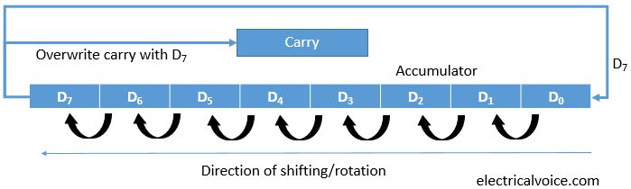

Manual Example of Accumulators

Introduction
These next set of instructions I’m about to show you are very similar; they all deal with what is known as “bit shifting”.
To explain the shifting process, we’ll use d0 as an example and make it contain 0000004C. We’ll take the byte 4C on the end, and look at it in bits:
0100 1100
|
When shifting the bits, there are two directions, left and right. So if we shifted the byte 4C left by 1 bit, we would get:
< 1001 1000 <
|
You can see the 0’s and 1’s have moved over 1 bit to the left. If we shifted 4C right by 1 instead, we would get:
> 0010 0110 >
|
The 0’s and 1’s have moved over 1 bit to the right. This is the standard idea of “bit shifting”.
Logical and Arithmetic shifting
When shifting bits to the left or right, an empty space is opened up, for example:
1100 1100
|
When shifting right by 1 bit, we get:
> ?110 0110 >
|
As the bits were shifted, the space on the far left (marked as ?) has appeared. The question is; is it filled with 0, or 1? This is decided by “logical”/“arithmetic”.
When using logical shifting, the answer is always 0:
> 0110 0110 >
|
When using arithmetic shifting, the answer is decided by the MSB (most significant bit). So, let’s just look at the byte before it was shifted:
1100 1100
|
As you can see, the MSB is 1. After an arithmetic shift:
> 1110 0110 >
|
The MSB stays as 1. If the bit were 0 on the other hand:
0100 1100
|
After an arithmetic shift:
> 0010 0110 >
|
The MSB stays as 0.
Here’s a graphical example of a logical shift “right”:

Here’s a graphical example of an arithmetic shift “right”:
For shifting “left” however, both logical shifting and arithmetic shifting have the same result, the LSB (least significant bit) always changes to 0:
1111 1111
|
After a logical or arithmetic shift left:
< 1111 1110 <
|

The result is always 0 no matter what the LSB was.

The CPU
A CPU is a processing circuit that can calculate, store results and makes algorithmic decisions. It is this latter factor that sets computers apart from calculators.
There are different CPU types, including:
- register machines
- accumulator machines
- stack machines
A very simple processor could be Jorvik-1, an accumulator machine:

The program counter is a register showing the current location in a set of instructions and the accumulator is where values are stored before and after computation.
An example set of instructions for this machine may be:
| Hexadecimal number | Assembler equivalent | Description |
| 31 | ADD A 03h | This is 0011 0001, so add 0011 and incremement the pc by 1 |
| F1 | SUB A 01h | Subtract (this is only possible if the accumulator understands signed numbers) |
| 05 | BRANCH 05h | The accumulator is not affected, but the pc increases by 5 |
| 01 | NOP | No operation, just continue to the next step (this can be useful for timing purposes) |
| 11 | INC A | Increment (really it's just add 1) |
| 00 | HALT | Don't increment the pc, and have no effect on the accumulator. |
However, what is wrong with Jorvik-1?
- The instruction set is very limited
- Is it actually useful?
What features should a CPU have?
- Ability to perform operations
- Add
- Subtract
- Possibly other operations
- Ability to choose what part of program to execute next
- Branch always
- Branch conditional
- Ability to access and alter memory access - with one register, auxilary memory access is essential
Most CPUs have many more features than this.
Jorvik-1 can not conditionally branch, or access memory, so it does not fit into these features.
Let's consider an improved processor - Jorvik-2.

Here, we have changed the format of the opcode, reducing the maximum size of a branch, but allowing conditional branching. When P = 0, the branch is always taken (pc = pc + ppp), however if P = 1, the branch is only taken if the accumulator = 0, otherwise the program counter is just incremented - so we now have a "branch if 0" instruction.
Complexity
Jorvik-2 is more complicated, so requires more hardware. If we consider the propogation delay in the gates, Jorvik-1 takes 25 ns per cycle (which works out as 40 MHz), whereas the same cycle on Jorvik-2 might take 70 or 75 ms, depending on specific implementation details, such as synchronisation between the accumulator and program counter stages. 75 ms is 13 MHz, which is a 3 times decrease in speed compared to Jorvik-1.
What does this tell us about complexity? Complexity is related to speed, therefore simple circuits run fast and complex circuits run slow. Jorvik-1 may be faster, but is not complex enough to be useful.
If a new feature is important and heavily used, the advantages may outweigh the speed cost. If the feature is only rarely useful, it may be a burden and slow down the whole CPU.
Addressing
Data can be held in memory and is normally organised into bytes (8 bits), words (16 bits) or double words (32 bits). Data can also be addressed directly as an operand in an instruction - for example ADD A 03h has an operand of 03h.
Instructions normally operate dyadically (they require two operands), e.g., ADD A 03h has two operands - Aand 03h. Having only one register (A) is not ideal and is not suited to the frequent case of dyadic operations. We should consider whether more registers would be better.
Our Jorvik-2 design is an extreme example of an accumulator machine - all operations use the accumulator (A) and a secondary operand. Having more registers will make our CPU more useful. We have already discussed 0 (stack), 1 (accumulator) 2 and 3 register addressing in operands in ICS, but adding more registers means complex and potentially slower circuitry. Adding fewer registers is normally simple and fast, but it could lead to harder programming, perhaps producing slower circuitry.
A Three Port Register File
Consider a three port register file of four 8-bit registers.

Accessing any three of these 4 registers simultaneously can create design problems. Reducing to two or one register addressing can ease the problem. Instructions must contain both the function code (ADD, SUB, etc) and the register addressed: FFFF XX YY ZZ - FFFF is the function code and XX YY ZZ are the registers (two inputs and an output) (as in the diagram above) - this is 10 bits long.
A One Port Register File

This is the standard accumulator model. It is much simpler, only one register file port is needed. Instructions contain one register address, the second register is always the accumulator. An instruction on this kind of machine looks like: FFFF RR - 6 bits long.
No Registers - The Stack Model
The stack (or zero-operand) model has no addressable registers, and thus no register file in the traditional sense.

Instructions only specify the function code (e.g., ADD, SUB, etc). Registers are always TOP and NEXT by default. An instruction in this model is only 4 bits long: FFFF.
We can implement a stack based on our Jorvik-3 machine, which adds an L (load) bit to the opcode which allows us to load something (a number bbb) onto the stack. However, we have lost a bit from our function code and introduced delays due to new components.

Upon examining Jorvik-3 we start to see some new instructions when we examine the circuitry. We have a new SET instruction which pushes a value onto the stack, and ADD, which adds two values from the stack together. However, our design only has a data adder in the path, so we can no longer do SUB. To get round this, we can SET a negative value onto the stack and then ADD.
Jorvik-3 has new features, however they come at a cost. We could work around this cost in various ways:
- making our instruction set 16 bit rather than 8
- improving the way branches are handled - most CPUs don't combine branches with arithmetic operations, and branch:arithmetic functions are in the ratio of approximately 1:6, meaning we're wasting about 40% of our bits in unused branches.
Having other functions would also be nice - a SUB function in addition to ADD, also AND and OR and the ability to DROP things off the stack would also be useful.
It would be difficult (not to mention slow) to introduce these features to our existing Jorvik-3 architecture, so we need another technology shift to Jorvik-4.

Instructions
Additional information is available on the instruction decoder on the CAR course pages.
The biggest advantage to the Jorvik-4 architecture over our previous architectures is that the opcode is now 8-bits long. We've already discussed what a CPU should have, but what other things are important in an architecture? Common sense and quantative data tells us:
- Speed of execution
- Size of code in memory
- Semantic requirements (what the compiler or programmer needs).
Decoding Instructions
Jorvik-1 through 3 used unencoded instructions - sometimes called external microcode. Each bit of the function maps directly onto internal signals.
The Jorvik-4 architecture uses an encoded instruction format. The 8-bit opcode is just an arbitary binary pattern, of which there are 256 possible permutations to decide which signals are to be applied internally. An internal circuit (the instruction decoder) does this, but wastes time doing it. There are two decoding strategies to use with an instruction decoder, either using internal microcode - a ROM lookup table that outputs signals for each opcode or hardwired - a logic circuit that directly generates the signals from opcode inputs. Microcode is easier to change, but hardwiring is usually faster.
Whether or not we use microcode or hardwiring, there is going to be a decoding delay. Suppose an ALU operates in 20ns, but a decoder takes 10ns, that means each operation takes a total of 30ns, or 33 million operations per second. However, with a clever design, we can overlap instructions, so the decoder can start decoding 10ns before the ALU is due to end the previous operation, meaning that the new instruction will be ready for as soon as the ALU finishes.
An encoded instruction format relies upon an opcode of n-bits, and each permutation is a seperate function. However, it is often useful to sub-divide functions in the opcode. We also need to consider the frequent requirements for data operands. We could assume that any operands will be stored in the memory byte immediately following the opcode. ADD and SUB are 1-byte instructions requiring only one opcode byte, but SETis a 2-byte instruction, requiring opcode and operand.
At the moment, Jorvik-4 is only an architecture - there is no defined instruction set. From our earlier machines, we almost certainly need to include the following instructions:
| Instruction | Description |
| SET nn | Push nn onto the top of the stack |
| ADD | Add the top two values of the stack together |
| SUB | Subtract the top two items together (NEXT - TOP) |
| BRANCH nn | Branch back or forward by nn place unconditionally |
| BRZERO nn | Branch back or forward by nn places if zero is detected |
| NOP | No operation (normally included by convention) |
| STOP | Stop execution |
We can see here which instructions are 2 bits and which aren't.
Delays
In addition to the delay we saw introduced by the instruction decoder, there are also delays introduced by memory latency. These include a delay from fetching an instruction (instruction fetch, or IF), and also a possible additional delay caused by fetching an operand (data fetch, or DF).
Our timing diagram for a SET operation may look like:

However, we can not assume that delays just add up to a final figure. Clocks usually have a uniform clock period, so our operations must be timed with clock ticks.

Here, decode is given 15ns, rather than the 10ns it needs and the operation execution has 30ns, instead of 20, leading to wasted time. A more sensible clock period may be 10ns.
Now that we've taken into account memory latency, we need to reconsider our overlapping time-saving technique. Only one fetch (instruction or data) can happen at once, so we need to wait for one IF to finish before starting the next one, but we can overlap the IF with the decode procedure and then overlap the decode as before. However, if the instruction is a two-byte instruction and requires a DF also, we're in trouble. We can't start the next IF until that DF has finished, and as the IF and decode operations take longer than the execution of operation, we still end up waiting, negating the effects of our overlapping. Therefore, we want to avoid 2-byte operations whenever possible.
SET is a frequent operation, but common sense tells us that frequent operations should be fast and compact, so we should look at ways to improve the performance of this command. Patterson & Hennessey tell us that at least 40% of constants are 4 bits or less, and 0 and 1 are very commonly used. We could improve matters in varying approaches:
- Maybe we could have a special short set instruction (SSET n as well as SET nn)
- A special "Zero" opcode could be used to initialise a zero onto the stack
- We could replace SET 01h, ADD with a special INC function.
- We could also replace SET 01h, SUB with a special DEC function.
If we decide to have a SSET function, we must consider how this would work in practice on an 8-bit instruction set. If we have XXXX dddd, this gives us 4 bits of opcode and 4 bits of data and SSET values 0-15. This is too restrictive, as we would only have 16 instructions available, each with 4 bits of data.
However, we could only have dddd when XXXX = 1111, so opcodes 00h to EFh are unaffected and we still have 240 possible opcodes, and then opcodes F0h to FFh give us SSET 0h to SSET Fh. As F0h is SSET 0h, we don't need a special "initialise 0" function any more.
The Stack
We covered the concepts of stack-based computing in ICS. Let's consider that we want to calculate the average of three numbers, X, Y and Z.
| Instruction | Stack Content |
| SET X | X |
| SET Y | Y X |
| ADD | Sum1 |
| SET Z | Z Sum1 |
| ADD | Sum2 |
| SET 3 | 3 Sum2 |
| DIV | Average |
Here, we've added yet another command - DIV, which divides. However, if DIV does 3 ÷ Sum2 instead of Sum2 ÷ 3, we have a problem.
Stack order affects a computation, so we should add commands that manipulate the stack.
- SWAP - this swaps the top two elements of the stack so X Y Z becomes Y X Z
- ROT - this rotates the top 3 items on the stack so X Y Z becomes Z X Y
- RROT - this rotates the stack in the opposite direction, so X Y Z becomes Y Z X
Re-using Data Operands
Say we have the formula (A - B) ÷ A, we can see that A is used twice, but in our current instruction set, this would require 2 fetches of A into our stack, and as every fetch introduces a delay penalty, this might not be the optimal solution. Using our current instruction set, an implementation of this may use 9 bytes of storage and 3 fetch delays.
We could implement a DUP operator which duplicates the top of the stack.
| Instruction | Stack Contents |
| SET A | A |
| DUP | A A |
| SET B | B A A |
| SUB | Sum1 A |
| DIV | Result |
| STOP |
This requires 8 bytes of storage and only 3 fetch delays.
Another useful command would be the DROP instruction, to throw away the top stack item, so X Y Z becomes Y Z, for example.
Another approach to stacks is orthogonality and scalability, of which more information is available in the original lecture slides.
Branches
All architectures have some form of branches. We could use them for:
- skipping over parts of a program - normally conditional
- jumping back repeatedly to a certain point (i.e., a loop) - normally conditional.
- moving to another part of the program - normally conditional
In cases 1 and 2, the branch will probably be quite short. In case 3, the branch distance could be quite large. According to Patterson and Hennessey, 50% of branches are ≤ 4 bits (based on 3 large test programs). These are almost certainly mostly types 1 and 2.
If all branch operations were 8-bit, we'd need 2 bytes for every branch and 2 fetches. However, if we have short 4-bit operand, then 50% of brances will be 1 bit only.
The most common type of branch is a relative branch - these are normally used within loops. They test a condition and loop back is true. Brances are used to skip over code conditionally.
Long Branches
Long branches are used to jump to another, major part of a program. Normal branches have a limited range, of about 27 (7-bits and a sign bit), so long branches use a fixed (absolute) 2-byte address (16 bits). Long branches get relatively little use, compared to other branching methods. Long branches have been replaced in a lot of cases by procedural code.
Indirect Branch
A memory address is given in the branch opcode. The memory address contains where to jump to, rather than the opcode. e.g., IBranch 06h would jump to the address stored at location 06h.
Such branching schemes are speciallised (sometimes called a jump table), but can speed up cases where there are multiple outcomes to consider (e.g., a 'case' in higher level programming languages). IBranch could also be implicit, using the value on the top of a stack.
ALU
The ALU is the Algorithm and Logic Unit. It is capable of monadic (1 operand) and diadic (2 operand) operations. The ALU requires operands and a function code (to tell it what to do).
The ALU is used for performing calculations (some are floating point, others integer only), manipulating groups of bits (AND, OR, XOR, NOT) and for testing conditions (test-if-equal, test-if-greater, test-if-less,test-if-zero, etc).
The ALU also has a carry flag which occurs when arithmetic takes place if the result is too large to fit in the available bits. The carry flag "catches" the final bit as it falls off the end.
Software vs. Hardware
A hardware multiply instruction may be very fast (1 cycle), but requires complex circuity. It can also be done in software using two methods:
- repeated addition: 10 × 3 = 10 + 10 + 10
- shift and add: 10 × 3 = (3 × 0) + (30 × 1)
Calls, Procedures and Traces
Programs consist of often repeated sequences, or 'routines'. An in-line routine is coded at each point when they are needed - this is inefficient on memory use.
In a real program, a common routine may be done 100s of times, so doing it in-line may result in an increased possibility of bugs. Complicated procedures may takes 10s or even 100s of lines of instructions.
How can we avoid this repetition? One answer is to branch to one part of the program and then branch back when finished. If we store this return value (where to go back to) somewhere, we know where we'll be going back to.
To implement this in our architecture, we need new instructions:
- CALL nnnn - this stores the current pc somewhere and branches to the specified address
- RETURN - this gets the stored pc value and branches back to that address (the stored pc value should really be the instruction after the original CALL, otherwise you would end in an endless loop).
We now have a smaller program with greater consistency in code, however the CALL and RETURN have overhead.
Hardware Considerations
To implement this, we need to consider how we will store the return value. One way is to just have a second pc register, which allows single level depth, but this is limiting. Adding a stack to the pc to allow multiple level calls (nested procedures) is more flexible. This is often called a program stack or return stack.
Now we need to consider how our instructions work. CALL would push pc + i (where i is the instruction length of the call operand - i.e., in a 16-bit address this would be pc + 3. Many architectures automatically increment the program counter after the instruction fetch anyway so often this isn't something to worry about) onto the stack and put the new address (operand of CALL) into the pc register. The machine then automatically goes to and executes the address in the pc.
For the RETURN instruction, the value on the top of the stack is popped onto the pc and the machine automatically follows this new instruction.
Traces
Traces are a useful hand debugging tool, especially for debugging loops. You act as the CPU, listing each instruction in order of execution, alongside the stack contents. From this you can check that the program behaves as expected, and possibly identify bugs in the architecture.
Long vs. Short
Usually CALL instructions have 16-bits (or longer) operands, however important routines - sometimes referred to as 'kernel' or 'core' routines - get called very often. These could be I/O procedures such as reading a byte from the keyboard or updating a display character or low-level routines such as multiply (if it's not implemented in hardware).
We could implement a 'Short Call' instruction, like SSet and SBranch. However, this gives us only 16 possible addresses. Each number should represent a chunk of memory, not a location, however - otherwise each instruction could only be 1 byte long.
Now our instruction set looks like this:
- F0 - FF SSet
- E0 - EF SBZero
- D0 - DF SBranch
- C0 - CF SCall
SCall 01 might call address 010000, SCall 02 100000, etc... - each address is bit-shifted so the instructions can be longer. If these addresses are at the beginning of memory, then SCall 00 is a software reset feature, as it runs the code at the very beginning of memory, rebooting the system.
So, implementing this in our new machine we get the final Jorvik-5, a dual-stack architecture.

However, additional hardware is required in the program counter path to figure out the new program counter value when incrementing in a call.
Addressing Modes and Memory
Addressing Modes were
also covered in ICS.
also covered in ICS.
An addressing mode is a method of addressing an operand. There are many modes, some essential, others specific. We have already used several addressing modes, consider:
- SET nn - the operand is immediately available in the instruction, this is called immediate addressing.
- BrZero nn - the address we want is nn steps away, relative to the present pc value -this is relative addressing.
- LBranch nn - the address we want is nn itself - this is absolute addressing.
- Skip - this is implicit, there are no operands
Implicit
This is typical with accumulator or stack-based machines. The instruction has no operands and always act on specific registers.
Stack processors are highly implicit architectures.
Immediate
Here, the operand is the data, e.g., Set 05 or SSet 6h (here, the operand is part of the opcode format).
The Jorvik-5 could make better use of immediate instructions, e.g., ADD nn adds a value onto the stack, instead of SET nn, ADD. This operation is a common one, so it may be worthwhile to implement this, although it does require hardware changes. We can justify this change if:
- it occurs frequently
- it improves code compactness
- it improves overall performance
In our current Jorvik-5 architecture, an instruction might requires 70 ns to execute. In our new design, each instruction now takes 80 ns to execute, but constants can be added with only one instruction. Taking into accounts fetches, our immediate add is now 30% faster, but we have a 14% slowdown for all other instructions.
We need to consider whether this trade off is worth it. If we plot a graph of speed-up against frequency of immediate add's, we need 30% of instructions to be immediate add's for the trade-off to break even, and 50% to gain even a modest 10% improvement.
Absolute
This form of addressing is very common.
To implement absolute addressing in our architecture, we need some new instructions:
- CALL nn - we've already covered this
- LOAD nn - push item at location nn onto the stack
- STORE nn - pop item off the stack into location nn.
Relative
This is commonly used for branches and speciallised store and load. The operand is added to an implicit register to form a complete address.
This is useful for writing PIC - position independant code. This kind of code can be placed anywhere in memory and will work.
Indirect
This addressing mode is more speciallised and less common. The operand is an address, which contains the address of the data to be accessed (an address pointing to an address). This is sometimes called absolute indirect.
Register Addressing
This is common in register machines. Here, registers are specified in the operands, e.g., ADD A B. Stack machines also have registers, mainly speciallised ones (e.g., the pc or flags such as carry and 0)
Register Indirect
This is a mixture of register and indirect addressing. Here, the register contains the memory location of data and then it works like indirect addressing.
High-Level Languages
High-level languages were developed in response to the increasing power of computers. It was becoming harder to write correct programs as the complexity of the instruction set increases. High-level languages come in two main types:
- Compiled to target - high-level language statements are translated into machine code and the program is executed directly by the hardware. This method can generate large programs.
- Compiled to intermediate form - high-level language instructions are compiled into an intermediate form (bytecode) and these intermediate forms need to be executed by an interpreter. This method tends to product machine-independant compact programs, but the interpreter also needs to be present.
The main requirement for an interpreter to be supported at machine level is the ability to execute one of many routines quickly. Each 'routine' defines a function in the language semantics. Ibranch allows us to branch to one of many subroutines, so we could implement an interpreter control loop with this. Each bytecode represents a location in the jump table, so we can use this to decide where to jump to to implement the instruction.
Typical languages consists of statements which we need to support in our machine architecture such as:
- Variables and assignment
- Conditional statements (if-then-else)
- Case (switch, etc).
Managing Variables
A few values can be kept on the stack or in registers, however most high-level languages have 100s of values to deal with. Registers and stacks are too small to support this, so we have to use main memory. We could store our variables at fixed addresses (e.g., X is 1000, Y is 1001, etc), but this is difficult to manage and wasteful as not all variables are needed at all times. We could store this values on another stack, so when they are created they are pushed onto the stack and when they are finished they can be dropped off. This type of implementation is known as a stack frame.
Stack Frames
Stack frames are needed for variables, as these need to be created and deleted dynamically and we have to keep variables in memory. Arrays are also variables and as such have the same issues, but they can contain many seperate data items. We need to consider how to manage the storage of these items effectively.
We also need to consider the program structure, which might consist of procedures and nested calls, recursion and interrupts. We can also have multiple instances of a procedure as multiple calls to the same procedure can co-exist.
Stack frames help as variables can be added to, or removed from, a stack. The stack resides in memory, but it can be located anywhere. For an array, the stack can hold a few, or many, bytes just as easily. As for the program structure, the stack frame can store the context of each procedure - recursive calls to procedures cause the preservation of the previous state. Multiple instances can also be implemented in the same way, where each call has its own state on the stack.
If we assume that we have a new third 'allocation' stack in Jorvik-5, then when a procedure is called, the first thing that happens is that variables are declared and created on the stack. If we had a procedure with 2 variables, A and B and an array X of length 4, then A, B, X[0], X[1], X[2] and X[3] are pushed onto the stack, on top of any data already on the stack. If our program was recursive, then we could get many stacks on top of each other and each one will maintain the correct state. Nesting is essentially the same principle, but a different procedure is called.
Our stack architecture has to place data on the stack to do computations, but the variables are held in memory - how do we get them onto the stack? A way to accomplish this is using indirect addressing. If we know a 'top-of-frame' address, then we can work out the address of a variable in memory.
We need another register to store a pointer to the top of the stack frame, which can be pushed onto the main stack for computation of indirect addressing. Because of the regularity of this process, we could have an indirect load instruction (LOAD (TOF)+02), if we figure it increases performance, however this is deviating from the stack machine philosophy. This kind of instruction does exist in register-based CPU, such as the 68000.
In high-level languages, there are more to variables than this, however. We have currently implemented local variables, which are created a procedural state and destroyed after the return and can only be accessed by the program that creates them, however we also have to consider global variables, which are usually created before the main procedure and can be accessed by any procedure at any time. So, our frame stack has to be accessible in two parts, one for globals and one for our current procedure (locals).
We can use a stack to store our pointers, so when we return, our stack frame can be restored. With this stack of pointers, we can access variables from higher levels.
Conditional Statements
To deal with conditional statements, we put the values to be compared on the stack, and then use a test operation (which sets the 0 flag is the test is true) and we can then do BrZero
Case Statements
Here, an Ibranch is used with a jump table.
Arrays
Arrays are typically placed in memory (in a stack frame or elsewhere) and access to the array is computed by using indexes to figure the offset from the array start.
Compilers
As we stated earlier, compilers turn high-level language statements into low-level machine code by recognising statements in the high-level language such as if-then and case and then outputting predefined machine code fragments.
Based on the examples given in the lecture slides, we could write a compiler for the Jorvik-5 and with a little work, a program could be written to recognise common statements and output Jorvik-5 machine code. There are various complications and refinements to be made, however, but the basic idea is there.
Interrupts
An interrupt occurs when a device external to the CPU triggers an interrupt request line (IRQ). The CPU responds with an IRQ acknowledge when it has processed the interrupt. An interrupt is a request from a device to the CPU to perform a predefined task, called the Interrupt Service Routine (ISR).
However, if there are several devices, things get more complicated. One option is to have an IRQ line for each device, but this leads to lots of CPU pins. An alternative is to allow all devices to share an IRQ line, but then we have to consider how to safely share one line.
Shared IRQ Approach
We have to somehow combine the IRQs from each device to signal an interrupt request. A tri-state OR gate can be used for this, however if more than one device triggers an interrupt, how does the CPU know which device needs servicing?
We can use the idea of interrupt prioritisation to work round this. A device has the idea of priority, and can only raise an interrupt if there are no more important devices requesting one. A method of implementing this is using daisy chaining, where a more important device in the chain lets the one directly below it know whether or not it (or any devices above it) want to use the interrupt, so the permission is passed down the chain. A single acknowledge line is used, with each device connected in tri-state. Only the device that generated the input pays attention to it.
However, we still have the problem of knowing which device initiated the interrupt, and which service routine to run.
Vectored Interrupts
To implement this, we can use vectored interrupts:
- A device triggers an interrupt
- The CPU acknowledges for more information
- The device issues a byte on the data bus
- The CPU reads the byte
- The byte can be an opcode, or vector address (jump table) - the exact details are architecture specific.
In Jorvik-5, we can use opcode interrupts where the short call uses a subroutine with I/O info. Each device has a different bit pattern for different opcodes. Negotiation is needed to ensure the correct subroutine is called.
Fully-Vectored Interrupts
If a single opcode is > 1 byte, then opcodes are tricky. A vectored address contains part of address with a subroutine in - e.g., an 8-bit vector (the VPN - vector page number) is combined with another 8-bit number (the VBA - vector base address) to give us the full adress. However, to make full use of the 8-bits we can only have 1 location per routine, which is not enough to be useful. Real systems use an interrupt vector table. The CPN is shifted so each location is 2 bits longer, combined with a 7-bits VBA. We can then use indirect addressing for our ISR as the actual instructions are in the 16-bit memory location given.
There are also other considerations we should make. We never know when an interrupt is going to be called, so the present state of the CPU needs to be preserved when the interrupt is called, and the ISR also needs to leave the CPU in the exact state is was before it started, otherwise program crashes may occur.
History of Computing
Ancient History
Abacuses were the most basic form of computing, and were thought to be invented by the Babylonians or the Chinese in 1000-500 BC. Common abacuses use base 5 or 10, and binary did not become the standard until the 1940s. In computing, binary is more stable, and less susceptible to noise (being either on or off, not laying inside certain band limits).
Charles Babbage (1791-1871)
Babbage is widely recognised as the father of computing and is most famous for designing the difference engine and analytical engine.
Difference Engine
The difference engine was commissioned by the British government to provide accurate logarithmic, trigonometric and other tables for their seafaring merchant and naval vessels. It could be considered to be an application specific computer (ASC) (i.e., optimised to provide one specific task). It worked by evaluation polynomials using the method of finite differences.
One of the main aims of the project was to cut out the human computer, thus removing any errors, therefore, the system needed to be able to print out the results to avoid any transcription errors - much like current times with automatic code generation.
The Difference Engine was constructed from a set of mechanical registers (figure wheels) storing differences Δ0 yi, Δ1 yi, ... and adding mechanisms and had eight storage locations with 31 decimal digits.
High levels of accuracy were required to minimise the effect of accumulated errors i.e., 31 decimal digits is equivalent to 103 bit arithmetic. Fractional numbers were multiplied by a constant i.e., scaled to fit within the machine�s integer representation and negative numbers were computed using complement notation.
To save cranking, and to speed up operations, the Difference Engine could be set for parallel "pipelined" operation. The maximum speed of the Difference Engine was 10 calculations a minute, or a result every 6 seconds. An attempt to run the system faster than this the momentum of some parts caused the transmission mechanism to bend, resulting in jamming or broken gear teeth.
In summary, the difference engine had register storage, addition with a ripple carry mechanism, a pipelined architecture and was capable of parallel operations.
Analytical Engine
Charles Babbage designed his analytical engine, which was the first programmable general purpose computer (although not stored program), however he never built it, due to lack of funds. It used microcode for complex operations. It was a lot bigger than the difference engine, and some designs went as far as 50 registers and 40 digit precision.
The main innovations were the seperation of storage and calculation units, giving us the Store (V) and the Mill, containing accumulators (A). Operations were controlled by the programmable card (consisting of operations cards, variable cards and number cards), and was based on the Jacquard loom. Babbage suggested using a printer, punched cards and a curve drawing machine as outputs, giving the machine both inputs and outputs.
The Analytical Engine used look-ahead carry, speeding up addition considerably (into a constant, rather than linear based on the length of the number), but 10 times more machinery was used for the carry than for the addition.
Electromechanical Machines (First generation relay and valve machines)
Konrad Zuse (1910 - 1995)
After Babbage's death, no serious attempts were made to build a general purpose computer until the 1930's. The first examples (the Z1 and Z3) were discovered after WWII and were found to be built in Germany between 1936-1941.
The Z1 machine represented numbers in a 22-bit floating point format and the arithmetic unit was an adder only (therefore subtraction could occur using complement notation) and all operations had to be reduced to addition. However, it was not very reliable, so the Z3 was constructed, which was made entirely out of relays and was programmed using punched tape and a user console.
The Z3 used microcode implemented using a micro sequencer constructed from stepwise relays and instruction overlapping was used (see earlier in notes - an instruction is read whilst result of last one was being written). A look-ahead carry circuit was constructed from relays which allowed fast addition to occur.
Harvard Mk I
The Mk I was developed by Howard Aiken and was built by IBM between 1939 and 1944. It was also known as the IBM Automatic Sequence Control Calculator (ASCC). It was constructed from electromechanical relays, was 55 feet long, 8 feet high, 2 feet deep and weighed 5 tons, making it relatively slow and very noisy. Numbers of up to 23 decimal places could be represented using electromagnetic decimal storage wheels - 3000 of which were present in the machine. The Harvard Mk I was used by the US Navy for gunnery and ballistic calculations until 1959 but it was out of date by the time it was commissioned.
Aiken went on to develop the Harvard Mk II, III and IV using valve technology, and he also developed the concept of the Harvard computer architecture, which uses physically seperate instruction and data memory. This allowed the next instruction to be read whilst the previous data is being written to memory and the width of the address and data bus could be different and optimised to the appropriate size. However, two memory modules were now required and storing programs inside the instruction memory could be difficult.
This is used in modern systems, where it is important to isolate the path between the processor and memory to maximise performance. Nowadays, a dual independent bus (DIB) is used. This replaces the system bus with a frontside bus (FSB), connecting the system memory (via the memory controller) to the CPU, and also to the other buses. The backside bus (BSB) is used to provide a fast direct channel between the CPU and the L2 cache.
ENIAC
ENIAC (Electrical Numerical Integrator and Computer) used valve technology instead of relay technology, and consumed 180 kW of power. It was commissioned by the US Army to calculate firing tables for specific weapons for a range of environmental and weather conditions. It was completed in May 1944, and has a strong claim to be the first ever general purpose electronic computer (although this is a topic of much debate). It was developed by a team lead by JP Eckert and JW Mauchly and was decimal, using over 18,000 valves and weighing 30 tons. It was much faster than anything ever built previously, and multiplication could occur in under 3 ms. It was described as being "faster than thought".
ENIAC was not a stored program computer, and needed rewiring if it was needed to do another job. For each program, someone needed to analyse the arithmetic processing needed and prepared wiring diagrams - a process which was time consuming and prone to error. This led to people such as John von Neumann to develop the idea of storing programs inside the computers memory - von Neumann originally envisioned programs which could modify their own program and rewrite itself. This innovation was a major factor that allowed computers to advance. This architecture was called the von Neumann architecture.
The von Neumann architecture used the same memory for instructions and data. The advantages of this was that a single memory module could be used, minimising the number of programming pins and buses. Instructions and data were treated equally, allowing data to be easily embedded into a program. However, this required the bandwidth of the memory bus to double and optimisations made by having seperate data and address bus sizes were lost.
Manchester Baby
This is sometimes referred to as the Small Scale Experimental Machine and it was the first ever electronic binary computer which executed its first stored program on June 24th 1948. It was created by a team at the University of Manchester between 1947 and 1949 consisting of Turing, Williams, Kilburn and Tootill. It had a 32-bit word length and used serial binary arithmetic using two's complement integers. It had a single address format order code and a random access main store of 32 words - extendable up to 8192 words. The computing speed was about 1.2 ms per instruction. It used Williams' idea of data storage based on cathode ray tubes (a Williams-Kilburn Tube) as the main store. This CRT had a big advantage over existing memory (delay line memory) as it allowed fast, random access to short strings of bits (i.e., 20-bit or 40-bit). The bits were stored as electrical charges on the phosphor of the CRT and had to be refreshed roughly every 0.2 s.
Delay line memory worked by electrical pulses being converted to sound pulses and then being transmitted down a long tube of mercury. A sufficient delay allowed a number of bits of data to be stored before the first bit was received and then re-transmitted. This was slow, serial and didn't allow random access to memory.
The Manchester Mark I had the first hard disk - two magnetic drums used for backing store. It was relatively slow, but had 16 times the storage of the CRT memory. The Manchester Mark I wsa the first to use a paging type memory store, where memory was divided into pages, each one containing 32 40-bit words (the size of a basic Williams-Kilburn tube) and was used as the unit of magnetic drum storage. In the Manchester Mk I, there was 4 pages of RAM main store and 128-page capacity of the drum backing store.
Each 40-bit addressable line could hold either 1 40-bit number, or 2 20-bit instructions.
EDSAC
EDSAC (Electronic Delay Storage Automatic Calculator) was built by Cambridge University in 1949. EDSAC stood out from its contemparies as it added microcode to the architecture, rather than the previous method of hardwiring control methods.
Collectively, these machines are referred to as the first generation computers and they share a similar system architecture. A typical example of the first generation machines was the IAS - a computer designed by von Neumann. The other major architecture of the time was the Harvard architecture.

This generation introduced isolating the processor from the IO with a dual independant bus architecture, replacing a single system bus with a frontside bus (FSB) and backside bus (BSB).
Second Generation Computers (Early Transistor)
The second generation of computing brought a change from valve to transistor and lasted between 1955 and 1964.
William B Shockley has been termed the "father of the transistor". He joined Bell Labs in 1936 in the vacuum tubes department before moving to the semiconductor department. The transistor is equivalent to a three-terminal electrical switch (triode). early transistors - point contact - were difficult to manufacture and were also unreliable. A few months later, work started on the junction transistor. Compared to valves, these were smaller, more reliable, faster and required less power.
The first experimental transistor computer was built in Manchester in 1953. It used 200 point contact transistors, 1300 point diodes and had a power consumption of 150 W. Main memory was implemented using a drum store, meaning that the transistor computer was slower than the mark one. The design was used as the basis of the MV950 in 1956, which was built using the more reliable junction transistors.
The next advance in this generation of computing was the non-volatile ferrite core memory. Each core had a diameter of about 2 mm and two magnetising wires and one sense wire passed through each one. The cores were arranged in a matrix such that each location was addressable.
A current passing through one of the magnetising wires would set a core magnetisation which could then be detected. Passing a current through the other wire would reset the magnetisation, giving either 1 or 0.
Many computers in this generation were transistor/valve hybrids, or just transistor implementations of the older valve computers. Another key part of this generation was the development of index registers and floating point hardware, the use of dedicated IO processors and hardware to supervise input/output operations, high level programming languages such as COBOL, FORTAN and large scale computer manufacturers also supplying compilers, software libraries with their machines.
Third Generation Computers
The IBM System/360 is the system which defines this generation of system - the classic mainframe computer system.
This machine used Solid Logic Technology (SLT), which was a transition between discrete transistors and integrated circuits. The System/360 also introduced an early form of pipelining to increase machine performance.
Concurrency is used to increase the number of operations that are happening simulataneously and there are two major approaches to this, temporal (the overlap of heterogenerous functional units) and spatial (the parallelism of homogenous units). The System/360 used temporal concurrency, known as pipelining for it's main performance increases, however spatial concurrency (parallelism) was used in some areas, such as addition, multiply and divide units. Dependancies could also come into play here, for example, one unit may be waiting on the result on the other, so some kind of mechanism must be used to stop register source/sink problems - the System/360 used highly speciallised dynamic scheduling hardware.
The System/360 used a microprogrammed control unit (from EDSAC), where each processor instruction in interpreted by a sequence of microinstructions called a microprogram.
The success of the transistor and other advances in solid state physics provided the foundation for another new technology - ICs, or integrated circuits. In 1958, Jack St. Clair Kilby whilst working at Texas Instruments succeeded in fabricating multiple components onto a single piece of semiconductor and hence invented the IC. In 1963, Fairchild invented a device called the 907 containing two logic gates constructed with 8 resistors and 8 transistors. SSI was born.
CMOS (Complementary Metal Oxide Semiconductor) logic was the next step. This formed TTL, and with no resistors, a higher density was possible.
The advent of cheap SSI, MSI and eventually LSI components allowed the development of minicomputers, such as the PDP-11, first developed in 1970.
Computers made from ICs could be generallised as the third generation of computers, and dominated from 1965-1971. In addition to the move from discrete transistors, semiconductor memory became to be in common use and microprogrammed CPUs became much more common. Multitasking operating systems were also invented
Fourth Generation Computers
In 1969, Marcian "Ted" Hoff, working for a small company producing memory IC called Intel, put a general purpose processor onto an IC and called it the 4004. It was a 4-bit processor in a 16-ping package (at the time, Intel could only produce 16-pin DIPs). The lower pin count meant a multiplexed address bus had to be used, simplifying the PCB as it required fewer connections, but adding complexity due to the multiplex logic.
Computers designed using this technology are referred to as fourth generation machines, and this became the dominant generation between 1971 and today. Here, circuits changed to VLSI and development became focussed on complicated "system on a chip" architectures.
Processor Design
Design Levels
Processor design requires consideration of all aspects of operation (software and hardware). For example, from a software point of view, we have A + B (High Level Language), which becomes Add A, R1 (Instruction Set Architecture, ISA) and then 01010100 (ISA implementation).
Processor design is based on levels of abstraction. As high level languages hides the details of the ISA from the programmer, the ISA hides the hardware implementation from the compiler.
At the hardware level, we can abstract further to give us three levels, the processor level (CPU, memory, IO and how these relate to each other), the register level (combinatorial logic, registers, sequential circuit) and gate level (logic gates, data buses, flip-flops, etc).
These classifications are hierarchial and lend themselves to a top-down design approach. A typical design process might be:
- Specify the processor level structure of the system that implements the desired ISA
- Specify the register level structure of each distinct component identified in step 1
- Specify the gate level structure of each distinct component identified in step 2
The first thing that needs to be done is to chose an ISA for the desired application (based on operand access):
- Stack based machines might be a Transputer T800
- Accumulator machines might be based on EDSAC or a 6502
- Register-memory machines might be based on the IBM 360 or 68000
- Register-register machines might be based on the MIPS or DLX
- Memory-memory machines might be a DEC Vax.
The key to a good processor design is to optimise performance based on instruction level simulations.
The next step is to define the ISA. This can be done in programs such as CPUsim where the ISA is defined as a sequence of microinstructions defining register level transactions.
A processors performance can then be evaluated in software against benchmarks before a CPU is implemented in hardware, allowing different architectures to be compared.
When top-down designing is used, components should be as independent as possible, allowing components to be designed and tested independently. Interconnection should be minimum where possible. Components that have high cohesion and low coupling will help design and testing. Additionally, component boundaries should correspond to physical boundaries, each design component should be a physically replaceable component, e.g., functional IC or PCB.
The processor level can be represented in a graphical way using a notation called PMS (processor, memory, switches) and block diagrams can be done using seven basic types:
- Processor (P), e.g., CPU, IOP
- Control (K), e.g., program control unit
- Data operation (D), e.g., arithmetic unit
- Memory (M), e.g., main, cache memory, etc
- Transducer (T), e.g., I/O devices
- Links (L), e.g., I/O port
- Switch (S), e.g., multiplexer, crossbar switching network
The symbol could also be qualified by a subscript, e.g., PIO may be a DMA controller.
VHDL
Before VHDL, boolean equations and logic was used to define a processor, similar to IDD/DAD. However, as processors became increasingly complex, schematic captures systems similar to PowerView were used, however as systems became bigger and more complex, this also became unmanagable, so hardware design languages (HDLs) - a textual description of the desired hardware - were used.
VHDL as an acronym is a combination of very high speed integrated circuit (VHSIC) and hardware design language (HDL). It was commisioned by the Department of Defense in America in the early 1980's as an implementation independent method of describing electronic systems. VHDL was based on Ada.
VHDL was primarily designed as a hardware modelling/specification language. It is used in all stages of design, from system level modelling of specification down to modelling the timing characteristics of implemented systems. Automated synthsis tools can be used to change VHDL into IC - i.e., these tools construct and optimise a gate level design into implementation.
As we design on different levels of abstraction, VHDL uses different styles depending on which level we're using. The two main styles are behavioural, which describes the function of the system as a black box where input and output timing relationships can be described in detail but with no indication of internal architecture (the system level), and register transfer level (RTL), where a design that is to be implemented physically on silicon has to be designed as a series of registers and interconnection signals and logic. This level describes the implementation's architecture (register level).
Implementations that are to be physically realised have to be written in the RTL style. Although tools can convert behavioural to RTL, this does not generally produce an optimal design.
Parallelism
To maximise software performance, a hardware architecture should be chosen to allow as many operations as possible to be perfomed in parallel. If the desired functionality can be decomposed into parallel processes, significant performance improvements can be made. However, this is based on the assumption that performing operations in parallel will requite a shorter time than performing the same operations sequentially. Althought this is essentially true, there are two key limiting factors in the performance of parallel architectures:
- The communications overhead, if data needs to be passed between processes. The Minsky conjecture states that the time wasted in synchronising and passing data between processes will reduce the system's performance.
- The parallel nature of the intended function is also a limiting factor (Amdahl's Law)
Amdahl's Law
Amdahl's Law gives us the speedup for p parallel processes, and is Sp = Ts/Tp, where Ts is the execution time of the algorithm on the sequential system and Tp is the execution time of the algorithm on a parallel system using p processors.
However, this is for an ideal algorithm - not all algorithms can be completely parallelised. If α is the fraction of the algorithm that can not be sped up in parallel with other processes, then: Tp = αTs + ((1 - α)Ts)/p, hence Sp = p/(1 + (p - 1)α). By setting the number of processors to infinity, we can calculate the maximum speedup of a system: Sp = lim 1/(1/p + (1 - 1/p)α) = 1/α.
Amdahl's Law states that the maximum potential speedup is limited by the sequential part of the algorithm that can not be parallelised.
Maximum speedup can only be acheived if a truly parallel architecture (a number of parallel processes operating independently of each other, with minimised inter-process communication) is constructed, minimising any sequential elements. The inter-dependencies that exist in the chosen algorithm determine if, and how, it can be partitioned into parallel processes.
Data Dependence
There are three main types of data dependencies that can exist between operations:
- Flow dependence, an operation (A) is dependent on another operation (B) if an execution path exists from B to A and if at least one output variable of A is used by B.
- Anti-dependence, operation B is anti-dependent on A if B follows A in the execution order and the output of B overlaps the input of A
- Output dependence: Two operations have output dependencies if they write data to the same variable.
Resource Dependencies
These dependencies arise from sharing conflicts of limited resources within a system. Typical examples are bus access, memory ports, register ports and functional hardware units. These are naturally sequential units that can not be accessed by more than one process at a time.
This type of dependency can be overcome by additional hardware, which increases complexity and cost.
In general, processes can operate in parallel if they fulfil Bernstein's conditions. For an operation A, with an input set of IA and an output set of OA, to operate in parallel with an operation B and the corresponding sets IBand OB, the following must be true.
- IA ∩ OB = ∅
- IB ∩ OA = ∅
- OA ∩ OB = ∅
The parallel relationship is represented by || and is commutitive and associative, but not transitive.
Concurrency
Concurrency can be implemented using spatial parallelism or temporal parallelism.
Spatial parallelism is when a number of processing modules are available to the controller. These can be internal to the processor (e.g., multiple ALUs) or external (i.e., multiple network cards, dual CPU motherboard).
Temporal parallelism is when the required functionallity can not be divided into totally independent processes, but can be divided into a number of independent processes, with flow dependencies. Each stage is dependent on the previous stage's output.
Pipelining
Pipelining is stealth parallelism - nobody realises it's there, but we use it every day. In unpipelined operation, one operation must complete before the next begins, but in pipelined operation, the next operation can start before the previous one finishes. For example, as soon as the instruction fetch stage has completed, you can start fetching the next instruction, as the memory is now not being accessed, but the decode stage is being used.
This allows for optimal use of the architecture by delaying waiting on something else.
Pipelining is acheived by breaking up the stages of the operation into seperate hardware sections seperated by registers that can keep state. The addition of registers increases the time for an operation to be processed, but as the throughput increases, more operations can be processed at once, increasing speed. The registers pass state up the pipeline.
However, hardware can not always be split up into units taking the same time, one process may take 15 ns for example, whereas another may only take 10. The clock speed is therefore limited by the slowest unit and an attempt must be made to balance the stages. There are two solutions to this, super-pipelining and a super-scalar architecture. Super-pipelining is splitting up a stage into two distinct units. This is not always possible, so super-scalar architectures can be used. Super-scalar architectures are when duplicates of the same hardware unit are used, which allows two operations to be processed at once, therefore stopping a stall for a particular hardware unit and increasing clock speed.
Deep pipelining is super-pipelining taken to the extreme, where the pipelines become very long (e.g., the Pentium 4 with a deep pipeline of 31). This leads to increased latency, and a new limiting factor comes into play - register and routing delays.
The speedup of a pipeline system is dependent on the number of stages within the pipeline, i.e., the number of operations that can be overlapped. In general, speed-up can be given by: time for a non-pipelined system / number of pipeline stages.
Hazards prevent the next operation from executing during its designated clock cycle, and can occur when the results from a previous operation or other result currently in the pipeline is required. This is called a sequential dependency and additional hardware may be needed to handle these situations. There are various different types of pipeline hazards:
- Structural hazards - these arise from resource conflicts when the hardware cannot support all possible combinations of instructions in simultaneous overlapped execution.
- Data hazards - these arise when an instruction depends on the result of a previous instruction in a way that is exposed by the overlapping of instructions in the pipeline
- Control hazards - these arise from the pipelining of branches or other instructions that change the pc.
Hazards have a very dramatic effect on the pipelines performance, reducing or removing any speedup gained by pipelining. Eliminating a hazard often requires that some instructions in the pipeline are allowed to proceed while others are delayed (stalled). A stall causes the pipeline performance to degrade the ideal performance.
A common measure of a processor's performance is the number of clock cycles required to execute an instruction (CPI). On a pipelined machine, the ideal CPI is 1, and the pipelined CPI can be given by 1 + pipelined clock stall cycles per instruction. We can then calculate speedup by the average time for a non-pipelined instruction / average time for a pipelined instruction, or (unpipelined CPI × unpipelined clock cycle time) / (pipelined CPI × pipelined clock cycle time). If we ignore the cycle time overhead of pipelining and assume all the stages are perfectly balanced, the cycle time of the two machines become unpipelined CPI / (1 + pipeline stall cycles per instruction). If all instructions take the same number of cycles equal to the number of pipeline stages (pipeline depth), then the unpipelined CPI is equal to the pipeline depth.
Structural Hazards
When a machine is pipelined, ideally we would want to be able to execute all possible combinations of instructions within the pipeline. The overlapped execution of instructions requires pipelining of the functional units and duplication of resources to allow parallel operations to be performed. If some combination of instructions can not be accommodated due to a resource conflict, the machine is said to have a structural hazard.
An example of this may be a single memory interface, where a LOAD operation may clash with the IF stage of another operation. To resolve this, the pipeline can be stalled for one cycle. The effect of a stall is to effectively occupy the resources for that instruction slot, i.e., a NOOP.
Introducing stalls does, however degrade performance, and for a designer to let structural hazards to occur, there must be a good reason. One is to reduce costs, multiple port memory is more expensive than single port, and other structural hazards may be solved by using more hardware. Another reason is to reduce latency, shorter latency comes from minimising pipeline hardware and registers.
Data Hazards
A side effect of pipelining instructions is that the relative timing between overlapped instructions is changed. Data hazards occur when the pipeline changes the order of read/write accesses to operands so that the order differs from the order seen by sequentially executing instructions on the non-pipelined machines, e.g., accessing data before a previous operation has finished writing it.
To solve this, you can detect when a data dependancy is going to happen (the input of one operation is going to be output by one already in the pipeline) and then stall all future instructions until the data is valid (i.e., revert back to a non-pipelined operation), however this is a massive performance hit. Another method is using a delayed read technique, in this technique, register file read operations are performed in the second half of the cycle and writes in the first half. By then ordering/timing the instructions correctly, writes will have happened before reads.
There are other methods also, forwarding data means extra hardware is used to move the registers contents between stages, for example, from the stage the data is written to the registers to the one where it is needed to be read. Control logic decides where the correct value should be in the chain and then when a read is requested, the value is returned from the correct set of registers, instead of the ones for that stage. This forwarding method requires an additional three results on the ALU multiplexor and the addition of three paths to the new inputs.
Data hazards can be classified into three types. If we consider two operations, i and j, with i occuring before j:
- Read after write (RAW) - j tries to read a source before i writes it, so j incorrectly gets the wrong value. This type of data hazard is the most common and can be solved with forwarding and delayed read techniques.
- Write after write (WAW) - j tries to write to an operand before it is written by i. The writes end up being performed in the wrong order, leaving the value written by i, instead of the value written by j in the destination. This hazard is present only in pipelines that write in more than one pipe stage or allow a n instruction to proceed whilst a previous instruction is stalled.
- Write after read (WAR) - j writes a new value before it is read by i, so i incorrectly gets the new value. This can not happen if reads are early and writes are late in our pipeline and this hazard occurs when there are some instructions that write early in the instruction pipeline and others that write a source late in the pipeline. Because of the natural structure of pipelines (reads occur before writes), such hazards are rare and only happen in pipelines for CISC that support auto-increment addressing and require operands to be read late in the pipeline.
By convention, the hazards are named after the ordering in the pipeline that must be preserved by the pipeline. Additionally, there is technically a fourth hazard, read after read (RAR), but as the state isn't changed here, no hazard occurs.
Another technique to overcome pipeline stalls is to allow the compiler to try to schedule the pipeline to avoid these stalls by rearranging the code sequence to eliminate hazards.
Control Hazards
In general, control hazards cause a greater performance loss for pipelines than data hazards. When a conditional branch is executred, there are two possible outcomes - the branch not being taken and the branch being taken.
The easiest method to deal with a conditional branch is to stall the pipeline as soon as the branch is detected until the new pc is known, however, wasting clock cycles at every branch is a huge loss. With a 30% branch frequency and an ideal CPI of 1, a machine with branch stalls only acheives about half of the ideal speedup from pipelining. The number of lost clock cycles can therefore be reduced by two steps:
- finding out whether the branch is taken or not taken earlier in the pipeline
- compute the target pc, i.e., the address of the branch target earlier
This can be acheived by moving the zero test into the ID stage, it is then possible to know if the branch is taken at the end of certain branches at that poin, or by computing the branch target address during the ID stage. This requires an additional adder because the main ALU, which has been used for this function so far, is not usable until the execution stage. Using the DLX architecture, a clock stall of 1 cycle is then needed. In general, the deeper the pipeline, the worst the branch penalty (stalled clock cycles) owing to the increased time to evaluate the branch condition.
To further minimise pipeline stalls caused by branches, branch prediction can be used. Analysing the execution of a program at run time, a guess can be made for each branch as to whether it will be taken or not. Four simple compile time branch prediction schemes are:
- stall prediction - the simplest scheme to handle branches is to freeze or flush the pipeline, holding or deleting any instructions after the branch until the branch destination is known. This simplifies hardware and compiler at the cost of performance.
- predict taken - as soon as the branch is decoded and the target address is computed, we assume the branch to be taken and begin fetching and executing at the target address. This method only makes sense when you know the target address before the branch output.
- predict not taken - higher performance, and only slightly more complex than stall prediction, you assume that the branch is not taken and simple allow the hardware to continue to execute. Care must be taken to not permenantly change the machines state until the branch outcome is definately known. The complexity arises from having to know when the state may be changed by an instruction and having to know when to back out of a change.
- delayed branch - during the branch delay of n cycles (delay slots) where the branch condition is executed, independent instructions are executed; the compiler inserts instructions into the branch delay slots which are executed whether or not the branch is taken. The job of the compiler (the hard part) is to make successor instructions valid and useful. Three common branch scheduling schemes are:
- from before branch - the delay slot is filled with an independent instruction from before the branch. This is the preferred choice, since this instruction will always be executed
- from target - the branch-delay slot is filled with an instruction from the target of the branch
- from fall through - the branch-delay slot is scheduled from the not taken fall through. For this and the previous optimisation to be legal, it must be okay to execute the instruction when the branch goes in the other direction
All the previous branch prediction schemes are static compiler based approaches to minimising the effect of branches. An alternative approach is to use additional hardware to dynamically predict the outcome of a branch at run time. The aim of this approach is to enable to processor to resolve the outcome of a branch early in the pipeline, therefore removing control dependencies in the program.
One method of doing this is using branch prediction buffers. The simplest example of this is a one bit memory array indexed by the lower order address bits. At each address a prediction based on the previous actions is stored. When an instruction is fetched, its address is looked up in the BPB during the ID stage. This returns a prediction for this branch (address), e.g., 0 means branch not taken and the next sequential address is fetched and 1 means the branch is taken and the branch target address is fetched. The processor assumes that this prediction is correct and acts accordingly. If the prediction is incorrect, the prediction bit is inverted and stored in the BPB and the pipeline is flushed. A two-bit branch prediction scheme is better for handling loops in loops as it requires two wrong guesses to actually change the state. Two bit prediction schemes allow more of the branch history to be remembered and the prediction to be more accurate. The performance of the BPB can be improved if the behaviour of the other previous branch instructions are also considered.
Branch predictors that use the behaviour of other branches are called correlating predictors or two level predictors. This type of predictor tries to identify larger patterns of execution (branch paths) in an attempt to predict the flow of execution.
Another hardware technique is the branch target buffer (BTB). At the end of the IF stage, the processor needs to have calculated the next address to be fetched. Therefore, if we can find out if the currently un-decoded instruction is a branch and can predict the result of that branch, then the branch penalty will be 0. During the IF stage when an instruction is being fetched, the pc address is also looked up in the BTB. If there is a match then this instruction is a branch and the predicted pc is used for the next IF. Unlike the BPB, the BTB must match the complete address, not just the lower order bits. Otherwise non-branch instructions could be misinterpreted as branches. The hardware used in this process is the same as that used for memory caches.
A typical BTB operation may work like this:
- If a match is found in the BTB, this indicates that the current instruction is a branch and is predicted as taken, therefore use the predicted pc for the next IF.
- If no match, but at the end of the ID, the instruction is determined to be a taken branch, then the PC and branch addresses are added to the BTB.
- If a match is found but the branch is determined not taken, then the entry is removed from the BTB, the incorrectly fetched instruction is stopped and then IF restarted at the other target address.
One final improvement that can be made to the BTB is to store one or more target instructions instead of, or in addition to, the predicted target address. This allows branch folding to be used, which allows zero cycle unconditional branches and some conditional branches. If a match is found in the BTB and it is determined that this instruction is an unconditional branch, then the stored instruction can be simply substituted.
Multicycle Operations
Until now, we have only considered a simple integer pipeline. In reality, it is impractical to require floating point operations to complete in one or two clock cycles. This would require the designer to accept a slow clock speed, use a large amount of floating point logic, or both. Instead, the floating point pipeline will allow for a longer latency for operations.
A super scalar architecture is used for floating point operations, however this leaves a longer latency, structural hazards where the floating point hardware can not be fully pipelined, WAW hazards for having pipelines of different lengths and an increase in RAW hazards due to increased latency.
Co-processors
General purpose processors attempt to provide a wide spectrum of support for applications. Inevitably, this will be less suitable for a particular application. This has led to the development of co-processor based architectures.
For each operation, the desired algorithms are divided between the CPU and its co-processors. This process is called hardware/software co-design, and there are four common strategies:
- Un-biased - the system is specified in an implementation independent manner with no presumption as to whether components should be implemented in software or hardware.
- Hardware biased - the system is realised in custom hardware except for those functions which can be executed in software and which still allow the systems to conform to the specified time constraints.
- Software biased - the system is implemented in software, except for those functions that need to be implemented in hardware to achieve the specific time constraints
- Hardware acceleration - The complete system is implemented in hardware as dedicated logic.
Partitioning of a system into its hardware and software components can be performed at a task, function block or statement level.
A CPU can interact with the co-processor using new opcodes - the CPU issues a command plus data sequence on its memory interface. This is identified and decoded by the co-processor. The CPU is either halted whilst this command is processed, or if possible, continues, being re-synchronised when the results are transferred. Additionally, remote procedure calls (RPCs) can be used, where the CPU again issues a command sequence, which is interpreted by the co-processor as an RPC. This is a similar process to the previous method, but with a more complex interface and tighter synchronisation.
Co-processors could also be implemented using the client-server model. The co-processor is configured as a server process, similar to the RPC mechanism. Data can now be processed from any process thread running on the CPU. The co-processor must arbitrate and prioritise between multiple requests. Another alternative is to specify the co-processor as the master, off loading tasks difficult to implement in hardware, or infrequent tasks, to the CPU more suited to dealing with these exceptions.
The final method is by parallel process - the co-processor runs as a top-level parallel process and communication between the two processors is a peer-to-peer arrangement.
The operations performed on the co-processor will normally require it to have access to variables and temporary storage. These can be implemented using various methods, such as:
- Having no external memory - data is either stored in specially constructed memory elements within the FPGA, or is explicitly stored as a result of the functions implementation. This increases the co-processors potential performance since no interface hardware is required to access external memory. This implementation is only possible for relatively small data sets, however.
- Sharing the CPUs memory - if truly parallel operation is not required, then the co-processor can use the CPUs memory, removing the communication delay of passing data. However, extra hardware that can negotiate with the CPU to gain access to this memory is required. This memory will have relatively slow access time, reducing the co-processors performance.
- Dual-port memory - this is based on SRAM memory cells, but with two or more memory interfaces. This allows multiple simultaneous data accesses, fast access times. However, this is very expensive, limiting it to a small size.
- Local memory - this decouples the CPU and the co-processor allowing parallel operation. This does require the co-processor to have additional hardware to interface to the external memory as before, but now fast SRAM can be used to maximise the co-processors performance. However, data must now be copied to this memory before processing can start.
you'll be needing a modem—a device that lets your computer send signals back and forth along a telephone line. You need a different kind of modem to go online with a dialup connection, with broadband, or with a cellphone (mobile broadband). What exactly are modems and how do they work?
What is a modem?
Telephones are amazing: they can carry the sound of your voice from one side of the world to the other in a matter of seconds by making electricity flow down a wire. Telephones are also the power behind the Internet—without them, it would be almost impossible for most of us to go online.
The marriage of the telephone (a 19th-century technology) with the computer (a 20th-century innovation) was something of a shotgun wedding. Computer technology is largely digital: it involves storing, processing, and transmitting information in the form of numbers. But telephone technology is still partly analog: information is transmitted down phone lines as continuously varying electrical signals. How, then, do digital computers communicate across analog telephone lines designed to carry speech? Simple: they use modems, devices that turn digital information into analog sound signals for the telephone journey and then turn it back again at the other end. Think of modems as translators. Computers speak digital, and telephones speak analog, so you need modems to translate between the two.
Photo (above): A state-of-the-art HSDPA broadband wireless modem (sometimes called a "dongle") made by ZTE. You need one of these to surf the Net on a cellphone network.
Suppose you want to connect your computer to an Internet Service Provider (ISP) using an ordinary phone line. The computer at your end needs a modem to modulate its digital signals (add them on top of an analog telephone signal) so they can travel down the phone line just like the sound of your voice. Once the signals have reached the other end, they have to pass through a second modem, which demodulates them (separates them out from the telephone signal and turns them back into digital form) so the ISP computer can understand them. When the ISP computer replies, it sends its signals through a modulator back down the line to you. Then a demodulator at your end turns the signals back into digital form that your computer can understand.
A box that we call a modem thus contains two different kinds of translators. There's a modulator (for transmitting digital signals out down the phone line in analog form) and a demodulator (for receiving analog signals from the phone line and turning them back into digital form)—and that's why it's called a modem.
Modulation is simply a fancy name for transmitting information by changing the shape of a waveform. If you send information by making the peaks of a wave bigger or smaller, that's called amplitude modulation or AM (because the amplitude is the size of the wave peaks); if you send information by changing how often the peaks travel, that's frequency modulation or FM (because the frequency is the number of peaks that travel per second). You may have heard the terms AM and FM before, because they describe how radio signals travel. (You can read a slightly longer explanation of modulation in our article on radio.)
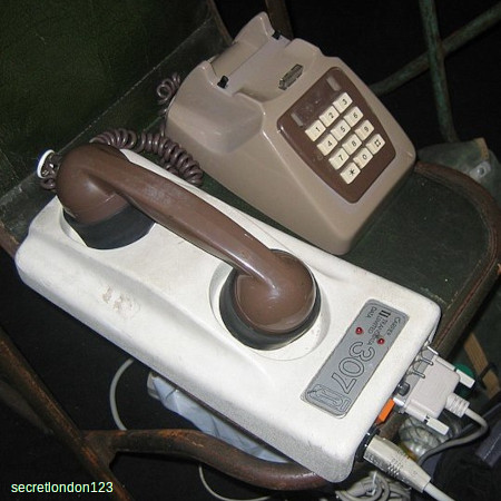
Photo: Modems as they used to look. This contraption is called an acoustic coupler and its built-in modem allows you to connect your computer to a network using an ordinary landline telephone. Devices like this were popular when people had phones that were hard-wired into connection boxes and couldn't be unplugged or switched for modern-style RJ11 phone jacks. In some countries, it was illegal to connect directly to the phone network, so couplers like this acted as handy intermediaries. Unfortunately, you have to dial manually with equipment like this—and in the early days, usually with a rotary dial phone, so making a connection could be a very slow business, especially if you dialled a wrong number. Photo by courtesy of secretlondon123 published on Flickr in 2008 under a Creative Commons (BY-SA) licence.
Controlling modems
Think of how you use the telephone. You don't just pick up the receiver and start talking. You have to go through a series of quite orderly steps: you have to lift the receiver, wait for the dialing tone, dial each number so it's recognized, wait for the sound of the ringing at the other end, listen for the other person's voice, say hello, and then alternate your speech with theirs. If there's no answer, you have to know when to replace the receiver and hang up the call.
Handshaking
Modems have to behave exactly the same way, exchanging information in a very orderly conversation. If you've used a dialup modem, you'll have noticed that your modem opens the line, dials the number, waits for the other modem to reply, and "handshakes", before any real data can be sent or received. If there's no reply, it'll hang up the line and tell you there's a problem. Handshaking is the initial, formal part of the conversation where two modems agree the speed at which they will talk to one another.
Standards and speeds
If you have a very fast modem but your ISP has only a slow one, the two devices will be forced to communicate at the slower speed. Every dialup modem works according to a particular international standard (a number prefaced by a capital letter V)—and this tells you how quickly it sends and receives data in bits (binary digits) per second (usually abbreviated bps). The most common standards are:
| Standard | Speed (bps) |
|---|---|
| V.22 | 1200 |
| V.32 | 9600 |
| V.32bis | 14,400 |
| V.33 | 14,400 |
| V.34 | 28,800 |
| V.34+ | 33,600 |
| V.90 | 56,000 |
| V.92 | 56,000 |
The older standards, such as V.22, assumed the connection between two computers was mostly analog; newer standards like V.90 achieve higher speeds by assuming the connection is at least partly digital.
Chart: Here's the same information from the table shown graphically. You can see that the most recent standards (like V.90) are about 4–5 times faster than the earlier ones.
Command sets
If you use the Windows operating system, you don't normally need to worry about how your modem communicates: it's all done automatically for you. But you can get your modem to send extra control commands, if you're having problems with it making calls. Using what's known as the AT command language (or the Hayes command set, for the company that invented it in 1977), you can change all kinds of other settings, including the maximum and minimum communication speed, how long the modem will wait before hanging up if the call is not answered, and so on. The exact commands you can use vary from manufacturer to manufacturer and from modem to modem, but a few are usually the same on every modem. For example, sending a command AT m0 almost always switches off the modem's loudspeaker so you don't get that irritating, electronic, handshaking chit-chat blasting out at you at the start of every session, while AT m1 keeps the speaker on until the connection is made (so you can check the handshaking sounds okay) and then disconnects it so you can enjoy some peace and quiet once you're online.
Different kinds of modem
Photo: A pair of dialup modems. On the bottom, our typical 56K dialup modem. On top, there's a 56K credit-card-sized PCMCIA modem for use in a laptop. The laptop card modem has no loudspeaker, LED indicator lights, or other advanced features but, in other respects, works the same way. It takes its power from the laptop's PCMCIA connection and needs no external power supply.
Hardware modems
External modems—ones you connect to your computer through a cable or PCMCIA socket—are examples of what we call hardware modems: the modem functions are carried out entirely by chips and other electronic components in hardware.
Dialup modems are probably the most familiar hardware modems, though few us use them these days. A dialup connection to an ISP uses circuit switching, just like an ordinary phone call. But if you're using broadband to get a faster connection, you'll use your phone line in an entirely different way, using a data-handling technique called packet switching—and you'll need an entirely different kind of modem. (Read more about circuit and packet switching in our article about the Internet.) If you want to use broadband (packet switching) on a cellphone network, you'll need yet another kind of modem (known as an HSDPA modem).
If you link to the Internet without using a telephone line, either by using a wired ethernet connection or Wi-Fi (wireless ethernet), you won't need a modem at all: your computer sends and receives all its data to and from the network in digital form, so there's no need to switch back and forth between analog and digital with a modem.
Dialup modems have another handy feature: they can communicate with fax machines at high speed. That's why they're sometimes called fax modems. If you have fax software on your computer, you can use your modem to fax out word-processed documents and receive incoming faxes.
Software modems
As their name suggests, software modems carry out virtually all of a modem's jobs using software. That makes them low-cost, compact, and easy to upgrade, so they're a particularly popular choice in things like laptop and netbook computers where space is at a premium. Software modems rely on the host computer's processor to carry out some of their functions, which means they slow a computer down more than an external hardware modem with its own built-in processor and dedicated chips. At its most extreme, a software modem is just a DAA (data access arrangement): the most basic part of a modem that makes the physical interface between the relatively high voltage analog phone line and public phone network (on one side) and the lower voltage, digital modem circuits (on the other), ensuring the two can safely talk to one another.
What are the parts inside a modem?
In theory
A modem is the "interpreter" between a digital computer and the traditionally analog phone network, which is sometimes (especially in technical books) referred to as the PSTN (public switched telephone network). The main components shown here are:
- Computer or computer network—entirely digital.
- Computer interface.
- Modem controller—essentially the modem's independent, central processor.
- Digital to analog converter (for outgoing, transmitted data)—turns computer data into phone-like analog signals.
- Analog to digital converter (for incoming, received data)—turns phone signals into digital computer data.
- Data access arrangement (DAA) makes modem's circuits compatible with the electrical requirements of the phone network.
- PSTN—the "analog" phone network (these days, it's also substantially digital!).
In practice
Lift the lid on a dialup modem and this is what you'll find inside:
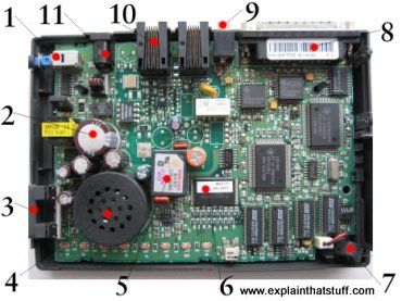
- On/off button: Spring-loaded switch turns the power on and off.
- Capacitors: Have a variety of jobs to do in a modem, including smooth out current peaks. (See our article on capacitors for more on how they work.)
- Volume control: Controls the loudspeaker volume.
- Loudspeaker: Relays what's happening on the phone line as your modem dials. Read more about loudspeakers.
- Modem chip: Modulates (add digital information to the outgoing telephone signal) and demodulates (separate the digital information from the incoming signal).
- Other chips: Control modem chip and other components.
- Microphone: Allows you to send your own voice down the phone line. Discover how microphones work.
- Serial connection: Connects the modem to your computer's serial (RS-232) port. Newer modems connect to the USB port instead.
- Microphone socket: Connects an external microphone so you can record messages in higher quality than if you use the built-in microphone.
- Telephone sockets: Connect your modem to a phone socket with a standard (RJ11) telephone cable. There's a second socket where you can plug a telephone handset into your modem. This lets you to use your phone through the modem when your computer's not already using the line.
- Power input: Connects the modem to an external power supply unit (electricity transformer) to your modem.
AC adapter

Recommended parts
GDT MOV SMD type CDA70-272M 470V Lead type CDA70LE272M , FA55-272 , DA53-272M
| GDT | MOV | |
| SMD type | CDA70-272M | 470V |
| Lead type | CDA70LE272M , FA55-272 , DA53-272M |
Telephone line / ADSL

Recommended parts
| SMD type | Lead type | |||
| GDT1 | CDA70-301L , CSA70-301L | DSS-301L | ||
| GDT2 | AC withstanding:none | CDA70-301L , CSA70-301L | DSS-301L | |
| AC withstanding | ACwithstandingtest AC1,000V×1min, AC1,200V×1min | CDA70-272M CDA70-302M | CDA70LE272M DSS-272M | |
| ACwithstandingtest AC1,500V×1min | CDA70-302M | CDA70LE302M FA55-302 DSS-302M | ||
| GDT3 | CDA70-301L , CSA70-301L | DSS-301L | ||
Sensor and data line

Recommended parts
| GDT | TSS | |
| SMD type | - | Silicon type Absorber:30V |
Ethernet (100BASE-TX / 1000BASE-T)

Recommended parts
| GDT | |
| SMD type | CDA70-301L , CSA70-301L |
| Lead type | DE37-301L , DSS-301L |
Coaxial cable(CCTV)

Recommended parts
| GDT | |
| SMD type | CDA70-301L , CSA70-301L |
| Lead type | DE37-301L , DSS-301L |
USB

Recommended parts
| GDT | |
| SMD type | CSA20-141N , CSA30-141N |
| Lead type | DSP-141N , DSP-201M |
Booster circuit (Satellite broadcasting, Television)

Recommended parts
| GDT | |
| SMD type | CDA70-301L |
| Lead type | DE37-301L , DSS-301L |
TV antenna circuit

Recommended parts
| GDT | MOV | |
| SMD type | CDA70-272M | 220V~270V(φ10) |
| Lead type | CDA70LE272M , DA53-272M FA55-272 , DSS-272M |
Modem: What is a Modem? Types of Modems
Modem is abbreviation for Modulator – Demodulator. Modems are used for data transfer from one computer network to another computer network through telephone lines. The computer network works in digital mode, while analog technology is used for carrying massages across phone lines.
Modulator converts information from digital mode to analog mode at the transmitting end and demodulator converts the same from analog to digital at receiving end. The process of converting analog signals of one computer network into digital signals of another computer network so they can be processed by a receiving computer is referred to as digitizing.
When an analog facility is used for data communication between two digital devices called Data Terminal Equipment (DTE), modems are used at each end. DTE can be a terminal or a computer.
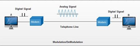
The modem at the transmitting end converts the digital signal generated by DTE into an analog signal by modulating a carrier. This modem at the receiving end demodulates the carrier and hand over the demodulated digital signal to the DTE.
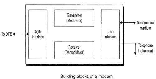
The transmission medium between the two modems can be dedicated circuit or a switched telephone circuit. If a switched telephone circuit is used, then the modems are connected to the local telephone exchanges. Whenever data transmission is required connection between the modems is established through telephone exchanges.
Ready to Send
To begin with the Data Terminal Equipment or DTE (better known as a computer) sends a Ready To Send or RTS signal to the Data Communication Equipment or DCE (better known as a modem). This is sometimes known as a wakeup call and results in the modem sending a Data Carrier Detect or DCD signal to the receiving modem. There then follows a series of signals passed between the two until the communication channel has been established. This process is known as handshaking and helps to explain why, even now, some companies like CompuServe use the symbol of two hands grasping each other to mean being on-line. Of course, after that all it takes is for the second modem to send a Data Set Ready or DSR signal to its computer and wait for the Data Terminal Ready or DTR reply. When that happens the first modem sends a Clear To Send or CTS signal to the computer that started the whole process off and data can then be transmitted. It is as simple as that.
Alternatively, for anyone confused by what the entire Internet industry dubs TLA's which means Three Letter Acronyms, the following diagram should help.
It only looks confusing. Take a second look and everything will soon become obvious.
By way of completeness, these signals are all sent through different pins in the plug which is why the handbooks for all modems and printers carry a pin diagram somewhere in the section on troubleshooting. They are also standardized after the industry leaders met to agree standards for a whole range of peripheral equipment. The Recommended Standard for cable was number 232 which explains that one technical term probably everybody has heard of: RS 232.
Of course, that still leaves the question of exactly how data is transferred from one computer to another; something that is more of a problem than might first appear mainly because the phone lines are analogue while computers are digital. In simple terms this means a telephone signal is constantly changing. To understand that just think of a sine wave as produced on an oscilloscope. The signal might be constant, but it is constantly changing from positive to negative and back again in a series of smooth curves. Computers, on the other hand, can only understand information when it is presented as a string of binary digits so the idea is to map digital output onto an analogue signal.
Without going into technical details this is done by superimposing different frequencies onto the analogue signal (which then becomes known as the carrier wave). Different frequencies can then represent different groups of binary digits in a process which is known as modulation when it is being transmitted and demodulation when it is decoded at the receiving end. Naturally two way communication is achieved by having a single device being capable of both modulation and demodulation, from which the unit takes its name: the modem.
From this it becomes obvious that the more frequencies that can be superimposed on the carrier wave the faster data can be transmitted. Alternatively, to take a different point of view, the more data there is to be transmitted so the more frequencies are needed.
Unfortunately it is only possible to send a limited number of frequencies at the same time, known as the bandwidth, which means communication takes that much longer as the size of the signals steadily increases. Now that pictures, sound and even video sequences are transmitted over the Internet on a regular basis, and as these all call for massive data files, the amount of available bandwidth is likely to be a problem for some time.
Finally, as the whole process comes down to sending binary digits or bits over a phone line the speed of the system is expressed as Bits Per Second or BPS which is a figure quoted by all the modem manufacturers.
Unfortunately when it comes to data communications there is a lot more involved than just how fast bits can be sent down a phone line. There is also the problem of what those bits mean and how they can be assembled into something intelligible at the far end. Here a whole range of issues need to be addressed and so it might be a good idea to briefly look at the first of these which are the transmission protocols.
Types of Modems
• Modems can be of several types and they can be categorized in a number of ways.
• Categorization is usually based on the following basic modem features:
1. Directional capacity: half duplex modem and full duplex modem.
2. Connection to the line: 2-wire modem and 4-wire modem.
3. Transmission mode: asynchronous modem and synchronous modem.
Half duplex and full duplex Modems
Half duplex
1. A half duplex modem permits transmission in one direction at a time.
2. If a carrier is detected on the line by the modem, I gives an indication of the incoming carrier to the DTE through a control signal of its digital interface.
3. As long as they camel' IS being received; the modem does not give permission to the DTE to transmit data.
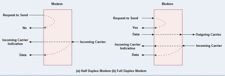
Full duplex
• A full duplex modem allows simultaneous transmission in both directions.
• Therefore, there are two carriers on the line, one outgoing and the other incoming. Wire and 4-wire Modems
• The line interface of the modem can have a 2-wire or a 4-wire connection to transmission medium. 4-wire Modem
• In a 4-wire connection, one pair of wires is used for the outgoing carrier and the other pair is used for incoming carrier.
• Full duplex and half duplex modes of data transmission are possible on a 4- wire connection.
• As the physical transmission path for each direction is separate, the same carrier frequency can be used for both the directions.
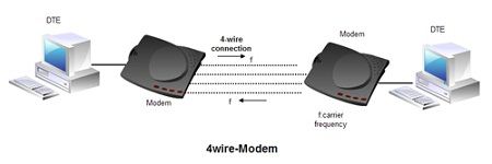
2-wire Modem
• 2-wire modems use the same pair of wires for outgoing and incoming carriers.
• A leased 2-wireconrlection is usually cheaper than a 4-wire connection as only one pair of wires is extended to the subscriber's premises.
• The data connection established through telephone exchange is also a 2-wire connection.
• In 2-wire modems, half duplex mode of transmission that uses the same frequency for the incoming and outgoing carriers can be easily implemented.
• For full duplex mode of operation, it is necessary to have two transmission channels, one for transmit direction and the other for receive direction.
• This is achieved by frequency division multiplexing of two different carrier frequencies. These carriers are placed within the bandwidth of the speech channel.
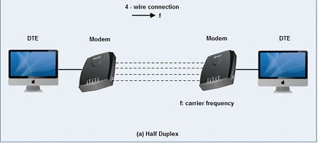
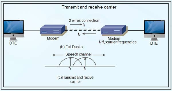
Asynchronous & Synchronous Modems
Asynchronous Modem
• Asynchronous modems can handle data bytes with start and stop bits.
• There is no separate timing signal or clock between the modem and the DTE.
• The internal timing pulses are synchronized repeatedly to the leading edge of the start pulse .
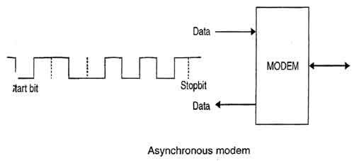
Synchronous Modem
• Synchronous modems can handle a continuous stream of data bits but requires a clock signal.
• The data bits are always synchronized to the clock signal.
• There are separate clocks for the data bits being transmitted and received.
• For synchronous transmission of data bits, the DTE can use its internal clock and supply the same to the modem.
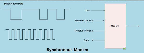
Modulation techniques used for Modem:
The basic modulation techniques used by a modem to convert digital data to analog signals are :
• Amplitude shift keying (ASK).
• Frequency shift keying (FSK).
• Phase shift keying (PSK).
• Differential PSK (DPSK).
These techniques are known as the binary continuous wave (CW) modulation.
• Modems are always used in pairs. Any system whether simplex, half duplex or full duplex requires a modem at the transmitting as well as the receiving end.
• Thus a modem acts as the electronic bridge between two worlds - the world of purely digital signals and the established analog world.
Network Connection Types
There are different types of communications connection in existence between two endpoints., Home networks, and the Internet is the one of the most commonly used examples. Many type of devices are and several different methods are used connecting to these type of network architectures.
There are different advantages and disadvantages to this type of network architectures. Connecting computers to a these type of networks, we requires some networking framework to create the connections. The two different computer network connection types are getting discussed in this page are Point-to-Point Connection and multipoint connection. The main difference between them we can getting discussed with the help of below definition.
Point-to-Point Connection
A point-to-point connection is a direct link between two devices such as a computer and a printer. It uses dedicated link between the devices. The entire capacity of the link is used for the transmission between those two devices. Most of today's point-to-point connections are associated with modems and PSTN (Public Switched Telephone Network) communications. In point to point networks, there exist many connections between individual pairs of machines.
To move from sources to destination, a packet (short message) may follow different routes. In networking, the Point-to-Point Protocol (PPP) is a data link protocol commonly used in establishing a direct connection between two networking nodes. It can provide connection authentication, transmission encryption, and compression PPP is used over many types of physical networks including serial cable, phone line, trunk line, cellular telephone, specialized radio links, and fiber optic links such as SONET. PPP is also used over Internet access connections (now marketed as "broadband").
Internet service providers (ISPs) have used PPP for customer dial-up access to the Internet, since IP packets cannot be transmitted over a modem line on their own, without some data link protocol. Two encapsulated forms of PPP, Point-to-Point Protocol over Ethernet (PPPoE) and Point-to-Point Protocol over ATM (PPPoA), are used most commonly by Internet Service Providers (ISPs) to establish a Digital Subscriber Line (DSL) Internet service connection with customers.
PPP is commonly used as a data link layer protocol for connection over synchronous and asynchronous circuits, where it has largely superseded the older Serial Line Internet Protocol (SLIP) and telephone company mandated standards (such as Link Access Protocol, Balanced (LAPB) in the X.25 protocol suite). PPP was designed to work with numerous network layer protocols, including Internet Protocol (IP), TRILL, Novell's Internetwork Packet Exchange (IPX), NBF and AppleTalk.
PPP is commonly used as a data link layer protocol for connection over synchronous and asynchronous circuits, where it has largely superseded the older Serial Line Internet Protocol (SLIP) and telephone company mandated standards (such as Link Access Protocol, Balanced (LAPB) in the X.25 protocol suite). PPP was designed to work with numerous network layer protocols, including Internet Protocol (IP), TRILL, Novell's Internetwork Packet Exchange (IPX), NBF and AppleTalk.
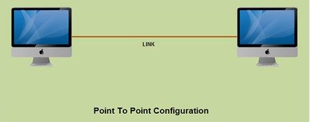
Multipoint Connection
A multipoint connection is a link between three or more devices. It is also known as Multi-drop configuration. The networks havjng multipoint configuration are called Broadcast Networks. In broadcast network, a message or a packet sent by any machine is received by all other machines in a network. The packet contains address field that specifies the receiver. Upon receiving a packet, every machine checks the address field of the packet. If the transmitted packet is for that particular machine, it processes it; otherwise it just ignores the packet.
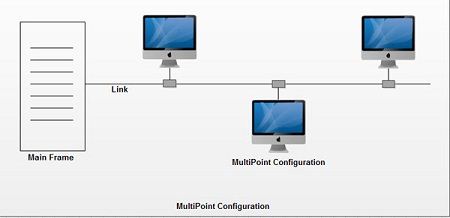
Broadcast network provides the provision for broadcasting & multicasting. Broadcasting is the process in which a single packet is received and processed by all the machines in the network. It is made possible by using a special code in the address field of the packet. When a packet is sent to a subset of the machines i.e. only to few machines in the network it is known as multicasting. Historically, multipoint connections were used to attach central CPs to distributed dumb terminals. In today's LAN environments, multipoint connections link many network devices in various configurations.
What is HTTP (Hypertext Transfer Protocol)?
What is http: HTTP full form HyperText Transfer Protocol used mainly to access data on the World Wide Web. HTTP is a Server and Client communication Protocol, which is primarily set of rules for formating and transferring webpage data (text, images, video and Multimedia files) over the world wide web. This is the Protocol used to create communication between Web Servers and Web Users. HTTP is an application layer Protocol that works on the top of the TCP/IP suite of Protocols.
HTTP protocol basically uses server and client model. It acts as a request-response protocol. For Example, A client which is use web browser and a server is a Web host that hosts the website. Whenever a client transmits a request to the Website server, HTTP protocol proceeds that request and creates a connection between client and server through TCP. After that HTTP sends a request to the server, which picks up the requested data and HTTP sends the response back to the client. Let's look into the depth how these requests work.
 HTTP protocol functions like a combination of FTP and SMTP. It is similar to FTP because it transfers files and uses the services of TCP. However, it is much simpler than FTP because it uses only one TCP connection. There is no separate control connection; only data is transferred between the client and the server.
 HTTP protocol is like SMTP protocol because the data transferred between the client and the server look like SMTP messages. In addition, MIME-like headers control the format of the messages. However, HTTP differs from SMTP in the way the messages are sent from the client to the server and from the server to the client. Unlike SMTP, the HTTP messages are not destined to be read by humans; they are read and interpreted by the HTTP server and HTTP client (browser). SMTP messages are stored and forwarded, but HTTP messages are delivered immediately.
The idea of HTTP protocol is very simple. A client sends a request, which looks like mail, to the server. The server sends the response, which looks like a mail reply, to the client. The request and response messages carry data in the form of a letter with MIME-like format.
The commands from the client to the server are embedded in a letter-like request message. The contents of the requested file or other information are embedded in a letter-like response message.
HTTP Request Methods
Http Protocol can use two case sensitive request-response Methods between client/server such as GET and POST that are used to handle form submissions.
GET Method
A GET Requests data from a specified resource using a given URI to retrieve data.
POST Method
A POST request Submits data to be processed to a specified resource to the server.
NOTE: URLs that start with "http://" are use port 80 by default and URL with "https://" are secure connection use port 443.
NOTE: URLs that start with "http://" are use port 80 by default and URL with "https://" are secure connection use port 443.
Differences between "GET" and "POST" Methods
"GET" is basically appends limited amount of variable and their values to the URL string because data is sent in header. It is non secure connection because variable and their values are exposed in URL.
"POST" appends large amount of data, because of data is sent in the message body.It is secure connection because variable and their values are not exposed in URL.
"POST" appends large amount of data, because of data is sent in the message body.It is secure connection because variable and their values are not exposed in URL.
What is an HTTP request?
A Http request message consists of a request line, headers and sometimes a body.
An HTTP request is a way that web browsers ask for information to load website pages. HTTP request contains HTTP version type, a URL, HTTP request headers and HTTP body.
HTTP request Headers: HTTP request headers include text information saved in key-value pairs and these are contained in every HTTP request.
URL: A client that wants to access a document needs an address. To facilitate the access of documents distributed throughout the world, HTTP protocol uses the concept of locations. The World Wide Web uses a locator called a URL to identify and intertribal data.
URL is called as (Uniform Resource Locator). A URL is an internet address of any website in common format http://ecomputernotes.com, A URL has three parts: Method: //Host/Path. which is used for accessing any file, document or website.
What is an HTTP response?
An HTTP response means when the web client gets the answer back from the web server. It contains the information that was asked for in the HTTP request. HTTP response contains an HTTP status code, HTTP response headers, and HTTP body.
HTTP status codes: Many times when a client sends a request to the server and If the HTTP request is not correct then the error comes. These errors are shown in numeric codes. These are also called as HTTP status codes. These status codes are given by the server to identify the problem. If a client does not know the difference between codes how a client can solve the problem so the client has to know about every code. Some common codes are shown below.
1.401-“Unauthorized”
2.400-“Bad request”
3.404-“File not found”
HTTP is a stateless protocol: HTTP is a stateless protocol and it was likewise necessary. Because it executes every command independently without knowing the other commands those came before it. Otherwise, if a client sends multiple requests to the web server, the web server will handle multiple requests from one connection for a long time. That's why HTTP is a stateless protocol.
What is HTTPS?
HTTPS is a Hyper Text Transfer Protocol Secure. This is the secure version of HTTP Protocol. HTTPS means a secure layer between client and server. HTTPS encrypted our data by Transport Security Layer (TLS). HTTPS is a sign of security most of the websites are secured with HTTPS.
(IP) Internet Protocol - What is Internet Protocol (IP)?
The Internet's basic protocol called IP for Internet Protocol. The objective of starting this protocol is assigned to interconnect networks do not have the same frame-level protocols or package level. The internet acronym comes from inter-networking and corresponds to an interconnection fashion: each independent network must transport in the weft or in the data area of the packet an IP packet, as shown in Figure.
There are two generations of IP packets, called IPv4 (IP version 4) and IPv6 (IP version 6). IPv4 has been dominant so far. The transition to IPv6 could accelerate due to its adoption in many Asian countries. The transition is however difficult and will last many years.
• Internet Protocol (IP) of network layer contains addressing information and some control information that enables the packets to be routed.
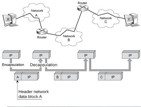
• IP has two primary responsibilities:
1. Providing connectionless, best effort delivery of datagrams through a internetwork. The term best effort delivery means that IP does not provides any error control or flow control. The term connectionless means that each datagram is handled independently, and each datagram can follow different route to the destination. This implies that datagrams sent by the same source to the same destination could arrive out of order.
2. Providing fragmentation and reassembly of datagrams to support data links with different maximum transmission unit (MTU) sizes.
IP packet format
• Packets in the network layer are called datagrams.
A datagram is a variable length packet consisting of two parts: header and data.
• The header is 20 to 60 bytes in length and contains information essential to routing and delivery.
• The various fields in IP header are:
1. Version: It is a 4-bit field that specifies the version of IP currently being used. Two different versions of protocols are IPV4 (Internet Protocol Version 4) and IPV6 (Internet Protocol Version 6).
2. IP Header Length (IHL): This 4-bit field indicates the datagram header length in 32 bit word. The header length i8 not constant in IP. It may vary from 20 to 60 bytes. When there are no options, the header length is 20 bytes, and the value of this field is 5. When the option field is at its maximum size, the value of this field is 15.
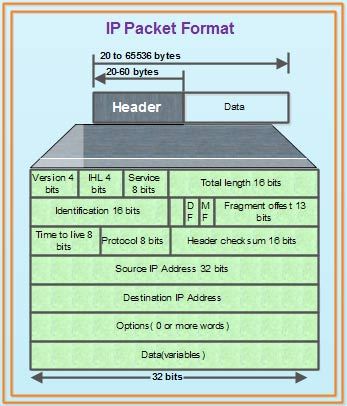
3. Services: This 8 hit field was previously called services type but is now called differentiated services.
The various bits in service type are:
• A 3-bit precedence field that defines the priority of datagram in issues such as congestion. This 3-bit subfield ranges from 0 (000 in binary) to 7 (111 in binary).
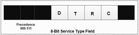
• After 3-bit precedence there are four flag bits. These bits can be either 0 or 1 and only one of the bits can have value of 1 in each datagram.
The various flag bits are:
D : Minimize delay
T : Maximize throughout
R : Maximize reliability
C : Minimize Cost
The various bits in differentiated services are:
• The first 6 bits defined a codepoint and last two bits are not used. If the 3 rightmost bits are 0s, the 3 leftmost bits are interpreted the same as the precedence bits in the service type interpretation.

4. Total length: This 16 bit field specifies the total length of entire IP datagram including data and header in bytes. As there are 16 bits, the total length of IP datagram is limited to 65,535 (216 - 1) bytes.
5. Identification: This 16 bit field is used in fragmentation. A datagram when passing through different networks may be divided into fragments to match the network frame size. Therefore, this field contains an integer that identifies the current datagram. This field is used to help piece together datagram fragments.
6. Flags: Consists' of a 3 bit field of which the two low order bit DF, MF control fragmentation. DF stands for Don't Fragment. DF specifies whether the packet can be fragmented MF stands for more fragments. MF specifies whether the packet is the last fragment in a series of fragmented packets. The third or high order but is not used.
7. Fragment Offset: This 13 bit field indicates the position of the fragment's data relative to the beginning of the data in the original datagram, which allows the destination IP process to properly reconstruct the original datagram.
8. Time to Live: It is 8 bit field that maintain a counter that gradually decrements down to zero, at which point the datagram is discarded. This keeps the packet from looping endlessly.
9. Protocol: This 8 bit field indicates which upper layer protocol receives incoming packets after IP processing is complete.
10. Header Checksum: This 16 bit field contains a checksum that covers only the header and not the data.
11. Source IP address: These 32-bit field contains the IP address of source machine.
12. Destination IP address: This 32-bit field contains the IP address of destination machine.
13. Options: This field allows IP to support various options such as security, routing, timing management and alignment.
14. Data: It contains upper layer information.
Wireless Principles
A cellular mobile communications system consists of a large number of low power wireless transmitters to create cells. These cells cover a certain area and typically called as base station. Depending upon the power level the size of cells can be decided. In this way, the radii of a cell may vary from tens of meters to tens of kilometers in a building to a city respectively.
It will also depend upon the subscriber density and demand within a particular area. The shape of cell may not be a perfect hexagon or circle and depends upon the environment. When a mobile user travels from cell to cell, their conversations are "handed oft'" between cells in order to maintain seamless service. Cells can be added as per the demands based upon the user density or newly created areas. Channels (frequencies) used in one cell can be reused in another cell after some distance and therefore it uses Space Division Multiplexing (SDM).
Frequencies for communication may vary from very high frequency (VHF) to microwave range. Regulation bodies of the concerned countries regulate these. The signal may be analog or digital with amplitude, frequency and phase modulation. The multiplexing and access techniques are space division multiplexing (SDM), frequency division multiplexing (FDM), time division multiplexing (TDM), and code division multiplexing (CDM).
The advantages of mobile communication may be looked into higher capacity, higher number of users, less transmission power needed, more robust, decentralized base station deals with interference transmission area etc. The disadvantages are fixed network needed for the base stations, handover (changing from 'one cell to another) necessary. Interference with other cells such Ii co-channel adjacent-channel.
It is now evident that cellular networks are, essential for wireless transmission. We ought to know about the cellular concept, frequency reuse, channel allocation, call setup, location management, cell handoffs, optimizations in terms of power control and cell capacity and implementations of GSM, GPRS, and 3G etc. The important issues on wireless communication 'are cell sizing, frequency reuse planning and channel allocations strategies.
What is a Distributed Computing System? - Definition
A Distributed computing is a model of computation that is firmly related to Distributed Systems, refers to as multiple computer systems located at different places linked together over a network and use to solve higher level computation without having to use an expensive supercomputer. Distributed system is called, When collection of various computers seems a single coherent system to its client, then it is called distributed system.
According to the definitions; All the computers are tied together in a network either a Local Area Network (LAN) or Wide Area Network (WAN), communicating with each other so that different portions of a Distributed applications run on different computers from any geographical location. Every node on the Distributed computing is autonomous machines (do not physically share memory or processors but thereby sharing resources such as printers and databases).
Distributed Systems have broken down into two parts: the front end and the back end. The front end, the part of the application that the user interacts with to determine what information she wants to examine and how to organise it, runs on the user's computer. The back end, the part of the application that finds and sorts the requested information, runs on a central computer somewhere else. This type of distributed computing also referred to as "client-server architecture," splits up the functioning of applications across some separate computers.
Grid computing is a based on distributed architecture and is the form of "distributed computing" or "peer-to-peer computing"that involving large numbers of computers physically connected to solve a complex problem.
Standalone applications are traditional applications(or 3-tier old systems) that run on a single system; distributed applications run on multiple systems simultaneously. Traditional applications need to be installed on every system and make it hard to maintain. However, In Distributed computing, applications run on both simultaneously. With distributed computing, if a workstation that goes down, another workstation can resume the jobs.
The advantages of distributed computing increased the speed with “absolute performance” and lower cost with more reliability than a non-distributed system. It is currently quite popular, and many businesses are converting to it as we speak.
Extremely well-known example of distributed systems and applications of distributed computing used in SETI@Home project of the University of California Berkley, Telecommunication networks, Telephone networks and cellular networks, Computer networks such as the Internet, Wireless sensor networks, Routing algorithms.
What is Hybrid networks?
• Hybrid networks are the networks that are based on both peer-to-peer & client-server relationship.
• Hybrid networks incorporate the best features of workgroups in peer-to-peer networks with the performance, security and reliability of server-based networks.
• Hybrid networks still provide all of the centralized services of servers, but they also allow users to share and manage their own resources within the workgroup.
Advantages of Hybrid Network
1. Client Server application are still centrally located and managed.
2. Users can assign local access to resources in their computers.
3. Workgroups can manage resources without requiring assistance from network administrator.
Disadvantages of Hybrid Network
1. Users may need to remember multiple passwords.
2. Files can be duplicated and changes overwritten between the computers with the shared folder and the Server.
3. Files saved on the workstation are not backed up.
The Internet of Things is an often discussed topic in magazines, there is no doubt that this market will grow significantly in the next years. Refer to the table below, in 2025 it is estimated that this market is more than three times larger compared to 2018.


+++++++++++++++++++++++++++++++++++++++++++++++++++++++++++++++++++++++++++++++++++++
e- SAW for ADA ( Address --- Data --- Accumulation ) on energy-efficient is cloud computing and Computer networking

+++++++++++++++++++++++++++++++++++++++++++++++++++++++++++++++++++++++++++++++++++++
Tidak ada komentar:
Posting Komentar