
Power electronics
Power electronics is the application of solid-state electronics to the control and conversion of electric power.
The first high power electronic devices were mercury-arc valves. In modern systems the conversion is performed with semiconductor switching devices such as diodes, thyristors and transistors, pioneered by R. D. Middlebrook and others beginning in the 1950s. In contrast to electronic systems concerned with transmission and processing of signals and data, in power electronics substantial amounts of electrical energy are processed. An AC/DC converter (rectifier) is the most typical power electronics device found in many consumer electronic devices, e.g. television sets, personal computers, battery chargers, etc. The power range is typically from tens of watts to several hundred watts. In industry a common application is the variable speed drive (VSD) that is used to control an induction motor. The power range of VSDs start from a few hundred watts and end at tens of megawatts.
The power conversion systems can be classified according to the type of the input and output power
- AC to DC (rectifier)
- DC to AC (inverter)
- DC to DC (DC-to-DC converter)
- AC to AC (AC-to-AC converter)


Power electronics started with the development of the mercury arc rectifier. Invented by Peter Cooper Hewitt in 1902, it was used to convert alternating current (AC) into direct current (DC). From the 1920s on, research continued on applying thyratrons and grid-controlled mercury arc valves to power transmission. Uno Lamm developed a mercury valve with grading electrodes making them suitable for high voltage direct current power transmission. In 1933 selenium rectifiers were invented.[1]
In 1947 the bipolar point-contact transistor was invented by Walter H. Brattain and John Bardeen under the direction of William Shockley at Bell Labs. In 1948 Shockley's invention of the bipolar junction transistor (BJT) improved the stability and performance of transistors, and reduced costs. By the 1950s, higher power semiconductor diodes became available and started replacing vacuum tubes. In 1956 the silicon controlled rectifier (SCR) was introduced by General Electric, greatly increasing the range of power electronics applications.
By the 1960s the improved switching speed of bipolar junction transistors had allowed for high frequency DC/DC converters. In 1976 power MOSFETs became commercially available. In 1982 the Insulated Gate Bipolar Transistor (IGBT) was introduced.
Devices
The capabilities and economy of power electronics system are determined by the active devices that are available. Their characteristics and limitations are a key element in the design of power electronics systems. Formerly, the mercury arc valve, the high-vacuum and gas-filled diode thermionic rectifiers, and triggered devices such as the thyratron and ignitron were widely used in power electronics. As the ratings of solid-state devices improved in both voltage and current-handling capacity, vacuum devices have been nearly entirely replaced by solid-state devices.
Power electronic devices may be used as switches, or as amplifiers.[3] An ideal switch is either open or closed and so dissipates no power; it withstands an applied voltage and passes no current, or passes any amount of current with no voltage drop. Semiconductor devices used as switches can approximate this ideal property and so most power electronic applications rely on switching devices on and off, which makes systems very efficient as very little power is wasted in the switch. By contrast, in the case of the amplifier, the current through the device varies continuously according to a controlled input. The voltage and current at the device terminals follow a load line, and the power dissipation inside the device is large compared with the power delivered to the load.
Several attributes dictate how devices are used. Devices such as diodes conduct when a forward voltage is applied and have no external control of the start of conduction. Power devices such as silicon controlled rectifiers and thyristors (as well as the mercury valve and thyratron) allow control of the start of conduction, but rely on periodic reversal of current flow to turn them off. Devices such as gate turn-off thyristors, BJT and MOSFET transistors provide full switching control and can be turned on or off without regard to the current flow through them. Transistor devices also allow proportional amplification, but this is rarely used for systems rated more than a few hundred watts. The control input characteristics of a device also greatly affect design; sometimes the control input is at a very high voltage with respect to ground and must be driven by an isolated source.
As efficiency is at a premium in a power electronic converter, the losses that a power electronic device generates should be as low as possible.
Devices vary in switching speed. Some diodes and thyristors are suited for relatively slow speed and are useful for power frequency switching and control; certain thyristors are useful at a few kilohertz. Devices such as MOSFETS and BJTs can switch at tens of kilohertz up to a few megahertz in power applications, but with decreasing power levels. Vacuum tube devices dominate high power (hundreds of kilowatts) at very high frequency (hundreds or thousands of megahertz) applications. Faster switching devices minimize energy lost in the transitions from on to off and back, but may create problems with radiated electromagnetic interference. Gate drive (or equivalent) circuits must be designed to supply sufficient drive current to achieve the full switching speed possible with a device. A device without sufficient drive to switch rapidly may be destroyed by excess heating.
Practical devices have non-zero voltage drop and dissipate power when on, and take some time to pass through an active region until they reach the "on" or "off" state. These losses are a significant part of the total lost power in a converter.
Power handling and dissipation of devices is also a critical factor in design. Power electronic devices may have to dissipate tens or hundreds of watts of waste heat, even switching as efficiently as possible between conducting and non-conducting states. In the switching mode, the power controlled is much larger than the power dissipated in the switch. The forward voltage drop in the conducting state translates into heat that must be dissipated. High power semiconductors require specialized heat sinks or active cooling systems to manage their junction temperature; exotic semiconductors such as silicon carbide have an advantage over straight silicon in this respect, and germanium, once the main-stay of solid-state electronics is now little used due to its unfavorable high temperature properties.
Semiconductor devices exist with ratings up to a few kilovolts in a single device. Where very high voltage must be controlled, multiple devices must be used in series, with networks to equalize voltage across all devices. Again, switching speed is a critical factor since the slowest-switching device will have to withstand a disproportionate share of the overall voltage. Mercury valves were once available with ratings to 100 kV in a single unit, simplifying their application in HVDC systems.
The current rating of a semiconductor device is limited by the heat generated within the dies and the heat developed in the resistance of the interconnecting leads. Semiconductor devices must be designed so that current is evenly distributed within the device across its internal junctions (or channels); once a "hot spot" develops, breakdown effects can rapidly destroy the device. Certain SCRs are available with current ratings to 3000 amperes in a single unit.
DC/AC converters (inverters)
DC to AC converters produce an AC output waveform from a DC source. Applications include adjustable speed drives (ASD), uninterruptible power supplies (UPS), Flexible AC transmission systems (FACTS), voltage compensators, and photovoltaic inverters. Topologies for these converters can be separated into two distinct categories: voltage source inverters and current source inverters. Voltage source inverters (VSIs) are named so because the independently controlled output is a voltage waveform. Similarly, current source inverters (CSIs) are distinct in that the controlled AC output is a current waveform.
DC to AC power conversion is the result of power switching devices, which are commonly fully controllable semiconductor power switches. The output waveforms are therefore made up of discrete values, producing fast transitions rather than smooth ones. For some applications, even a rough approximation of the sinusoidal waveform of AC power is adequate. Where a near sinusoidal waveform is required, the switching devices are operated much faster than the desired output frequency, and the time they spend in either state is controlled so the averaged output is nearly sinusoidal. Common modulation techniques include the carrier-based technique, or Pulse-width modulation, space-vector technique, and the selective-harmonic technique.[4]
Voltage source inverters have practical uses in both single-phase and three-phase applications. Single-phase VSIs utilize half-bridge and full-bridge configurations, and are widely used for power supplies, single-phase UPSs, and elaborate high-power topologies when used in multicell configurations. Three-phase VSIs are used in applications that require sinusoidal voltage waveforms, such as ASDs, UPSs, and some types of FACTS devices such as the STATCOM. They are also used in applications where arbitrary voltages are required as in the case of active power filters and voltage compensators.[4]
Current source inverters are used to produce an AC output current from a DC current supply. This type of inverter is practical for three-phase applications in which high-quality voltage waveforms are required.
A relatively new class of inverters, called multilevel inverters, has gained widespread interest. Normal operation of CSIs and VSIs can be classified as two-level inverters, due to the fact that power switches connect to either the positive or to the negative DC bus. If more than two voltage levels were available to the inverter output terminals, the AC output could better approximate a sine wave. It is for this reason that multilevel inverters, although more complex and costly, offer higher performance.[5]
Each inverter type differs in the DC links used, and in whether or not they require freewheeling diodes. Either can be made to operate in square-wave or pulse-width modulation (PWM) mode, depending on its intended usage. Square-wave mode offers simplicity, while PWM can be implemented several different ways and produces higher quality waveforms.
Voltage Source Inverters (VSI) feed the output inverter section from an approximately constant-voltage source.[4]
The desired quality of the current output waveform determines which modulation technique needs to be selected for a given application. The output of a VSI is composed of discrete values. In order to obtain a smooth current waveform, the loads need to be inductive at the select harmonic frequencies. Without some sort of inductive filtering between the source and load, a capacitive load will cause the load to receive a choppy current waveform, with large and frequent current spikes.[4]
There are three main types of VSIs:
- Single-phase half-bridge inverter
- Single-phase full-bridge inverter
- Three-phase voltage source inverter
Single-phase half-bridge inverter


The single-phase voltage source half-bridge inverters, are meant for lower voltage applications and are commonly used in power supplies.[4] Figure 9 shows the circuit schematic of this inverter.
Low-order current harmonics get injected back to the source voltage by the operation of the inverter. This means that two large capacitors are needed for filtering purposes in this design.[4] As Figure 9 illustrates, only one switch can be on at time in each leg of the inverter. If both switches in a leg were on at the same time, the DC source will be shorted out.
Inverters can use several modulation techniques to control their switching schemes. The carrier-based PWM technique compares the AC output waveform, vc, to a carrier voltage signal, vΔ. When vc is greater than vΔ, S+ is on, and when vc is less than vΔ, S- is on. When the AC output is at frequency fc with its amplitude at vc, and the triangular carrier signal is at frequency fΔ with its amplitude at vΔ, the PWM becomes a special sinusoidal case of the carrier based PWM.[4] This case is dubbed sinusoidal pulse-width modulation (SPWM).For this, the modulation index, or amplitude-modulation ratio, is defined as ma = vc/v∆ .
The normalized carrier frequency, or frequency-modulation ratio, is calculated using the equation mf = f∆/fc .
If the over-modulation region, ma, exceeds one, a higher fundamental AC output voltage will be observed, but at the cost of saturation. For SPWM, the harmonics of the output waveform are at well-defined frequencies and amplitudes. This simplifies the design of the filtering components needed for the low-order current harmonic injection from the operation of the inverter. The maximum output amplitude in this mode of operation is half of the source voltage. If the maximum output amplitude, ma, exceeds 3.24, the output waveform of the inverter becomes a square wave.[4]
As was true for PWM, both switches in a leg for square wave modulation cannot be turned on at the same time, as this would cause a short across the voltage source. The switching scheme requires that both S+ and S- be on for a half cycle of the AC output period.[4] The fundamental AC output amplitude is equal to vo1 = vaN = 2vi/π .
Its harmonics have an amplitude of voh = vo1/h.
Therefore, the AC output voltage is not controlled by the inverter, but rather by the magnitude of the DC input voltage of the inverter.[4]
Using selective harmonic elimination (SHE) as a modulation technique allows the switching of the inverter to selectively eliminate intrinsic harmonics. The fundamental component of the AC output voltage can also be adjusted within a desirable range. Since the AC output voltage obtained from this modulation technique has odd half and odd quarter wave symmetry, even harmonics do not exist.[4] Any undesirable odd (N-1) intrinsic harmonics from the output waveform can be eliminated.
Single-phase full-bridge inverter


The full-bridge inverter is similar to the half bridge-inverter, but it has an additional leg to connect the neutral point to the load.[4] Figure 3 shows the circuit schematic of the single-phase voltage source full-bridge inverter.
To avoid shorting out the voltage source, S1+ and S1- cannot be on at the same time, and S2+ and S2- also cannot be on at the same time. Any modulating technique used for the full-bridge configuration should have either the top or the bottom switch of each leg on at any given time. Due to the extra leg, the maximum amplitude of the output waveform is Vi, and is twice as large as the maximum achievable output amplitude for the half-bridge configuration.[4]
States 1 and 2 from Table 2 are used to generate the AC output voltage with bipolar SPWM. The AC output voltage can take on only two values, either Vi or –Vi. To generate these same states using a half-bridge configuration, a carrier based technique can be used. S+ being on for the half-bridge corresponds to S1+ and S2- being on for the full-bridge. Similarly, S- being on for the half-bridge corresponds to S1- and S2+ being on for the full bridge. The output voltage for this modulation technique is more or less sinusoidal, with a fundamental component that has an amplitude in the linear region of less than or equal to one[4] vo1 =vab1= vi • ma.
Unlike the bipolar PWM technique, the unipolar approach uses states 1, 2, 3 and 4 from Table 2 to generate its AC output voltage. Therefore, the AC output voltage can take on the values Vi, 0 or –V [1]i. To generate these states, two sinusoidal modulating signals, Vc and –Vc, are needed, as seen in Figure 4.
Vc is used to generate VaN, while –Vc is used to generate VbN. The following relationship is called unipolar carrier-based SPWM vo1 =2 • vaN1= vi • ma.
The phase voltages VaN and VbN are identical, but 180 degrees out of phase with each other. The output voltage is equal to the difference of the two phase voltages, and do not contain any even harmonics. Therefore, if mf is taken, even the AC output voltage harmonics will appear at normalized odd frequencies, fh. These frequencies are centered on double the value of the normalized carrier frequency. This particular feature allows for smaller filtering components when trying to obtain a higher quality output waveform.[4]
As was the case for the half-bridge SHE, the AC output voltage contains no even harmonics due to its odd half and odd quarter wave symmetry.
Three-phase voltage source inverter

_Switch_State_S1_b)_Switch_State_S3_c)_S1_Output_d)_S3_Output.jpg)
Single-phase VSIs are used primarily for low power range applications, while three-phase VSIs cover both medium and high power range applications.[4] Figure 5 shows the circuit schematic for a three-phase VSI.
Switches in any of the three legs of the inverter cannot be switched off simultaneously due to this resulting in the voltages being dependent on the respective line current's polarity. States 7 and 8 produce zero AC line voltages, which result in AC line currents freewheeling through either the upper or the lower components. However, the line voltages for states 1 through 6 produce an AC line voltage consisting of the discrete values of Vi, 0 or –Vi.[4]
For three-phase SPWM, three modulating signals that are 120 degrees out of phase with one another are used in order to produce out of phase load voltages. In order to preserve the PWM features with a single carrier signal, the normalized carrier frequency, mf, needs to be a multiple of three. This keeps the magnitude of the phase voltages identical, but out of phase with each other by 120 degrees.[4] The maximum achievable phase voltage amplitude in the linear region, ma less than or equal to one, is vphase = vi / 2. The maximum achievable line voltage amplitude is Vab1 = vab • √3 / 2
The only way to control the load voltage is by changing the input DC voltage.
Current source inverters

_Carrier_and_Modulating_Signals_b)_S1_State_c)_S3_State_d)_Output_Current.jpg)

Current source inverters convert DC current into an AC current waveform. In applications requiring sinusoidal AC waveforms, magnitude, frequency, and phase should all be controlled. CSIs have high changes in current overtime, so capacitors are commonly employed on the AC side, while inductors are commonly employed on the DC side.[4] Due to the absence of freewheeling diodes, the power circuit is reduced in size and weight, and tends to be more reliable than VSIs.[5] Although single-phase topologies are possible, three-phase CSIs are more practical.
In its most generalized form, a three-phase CSI employs the same conduction sequence as a six-pulse rectifier. At any time, only one common-cathode switch and one common-anode switch are on.[5]
As a result, line currents take discrete values of –ii, 0 and ii. States are chosen such that a desired waveform is output and only valid states are used. This selection is based on modulating techniques, which include carrier-based PWM, selective harmonic elimination, and space-vector techniques.[4]
Carrier-based techniques used for VSIs can also be implemented for CSIs, resulting in CSI line currents that behave in the same way as VSI line voltages. The digital circuit utilized for modulating signals contains a switching pulse generator, a shorting pulse generator, a shorting pulse distributor, and a switching and shorting pulse combiner. A gating signal is produced based on a carrier current and three modulating signals.[4]
A shorting pulse is added to this signal when no top switches and no bottom switches are gated, causing the RMS currents to be equal in all legs. The same methods are utilized for each phase, however, switching variables are 120 degrees out of phase relative to one another, and the current pulses are shifted by a half-cycle with respect to output currents. If a triangular carrier is used with sinusoidal modulating signals, the CSI is said to be utilizing synchronized-pulse-width-modulation (SPWM). If full over-modulation is used in conjunction with SPWM the inverter is said to be in square-wave operation.[4]
The second CSI modulation category, SHE is also similar to its VSI counterpart. Utilizing the gating signals developed for a VSI and a set of synchronizing sinusoidal current signals, results in symmetrically distributed shorting pulses and, therefore, symmetrical gating patterns. This allows any arbitrary number of harmonics to be eliminated.[4] It also allows control of the fundamental line current through the proper selection of primary switching angles. Optimal switching patterns must have quarter-wave and half-wave symmetry, as well as symmetry about 30 degrees and 150 degrees. Switching patterns are never allowed between 60 degrees and 120 degrees. The current ripple can be further reduced with the use of larger output capacitors, or by increasing the number of switching pulses.[5]
The third category, space-vector-based modulation, generates PWM load line currents that equal load line currents, on average. Valid switching states and time selections are made digitally based on space vector transformation. Modulating signals are represented as a complex vector using a transformation equation. For balanced three-phase sinusoidal signals, this vector becomes a fixed module, which rotates at a frequency, ω. These space vectors are then used to approximate the modulating signal. If the signal is between arbitrary vectors, the vectors are combined with the zero vectors I7, I8, or I9.[4] The following equations are used to ensure that the generated currents and the current vectors are on average equivalent.
Multilevel inverters
A relatively new class called multilevel inverters has gained widespread interest. Normal operation of CSIs and VSIs can be classified as two-level inverters because the power switches connect to either the positive or the negative DC bus.[5] If more than two voltage levels were available to the inverter output terminals, the AC output could better approximate a sine wave.[4] For this reason multilevel inverters, although more complex and costly, offer higher performance.[5] A three-level neutral-clamped inverter is shown in Figure 10.
Control methods for a three-level inverter only allow two switches of the four switches in each leg to simultaneously change conduction states. This allows smooth commutation and avoids shoot through by only selecting valid states.[5] It may also be noted that since the DC bus voltage is shared by at least two power valves, their voltage ratings can be less than a two-level counterpart.
Carrier-based and space-vector modulation techniques are used for multilevel topologies. The methods for these techniques follow those of classic inverters, but with added complexity. Space-vector modulation offers a greater number of fixed voltage vectors to be used in approximating the modulation signal, and therefore allows more effective space vector PWM strategies to be accomplished at the cost of more elaborate algorithms. Due to added complexity and number of semiconductor devices, multilevel inverters are currently more suitable for high-power high-voltage applications.[5] This technology reduces the harmonics hence improves overall efficiency of the scheme.
AC/AC converters
Converting AC power to AC power allows control of the voltage, frequency, and phase of the waveform applied to a load from a supplied AC system .[6] The two main categories that can be used to separate the types of converters are whether the frequency of the waveform is changed.AC/AC converter that don't allow the user to modify the frequencies are known as AC Voltage Controllers, or AC Regulators. AC converters that allow the user to change the frequency are simply referred to as frequency converters for AC to AC conversion. Under frequency converters there are three different types of converters that are typically used: cycloconverter, matrix converter, DC link converter (aka AC/DC/AC converter).
AC voltage controller: The purpose of an AC Voltage Controller, or AC Regulator, is to vary the RMS voltage across the load while at a constant frequency.[6] Three control methods that are generally accepted are ON/OFF Control, Phase-Angle Control, and Pulse Width Modulation AC Chopper Control (PWM AC Chopper Control).[8] All three of these methods can be implemented not only in single-phase circuits, but three-phase circuits as well.
- ON/OFF Control: Typically used for heating loads or speed control of motors, this control method involves turning the switch on for n integral cycles and turning the switch off for m integral cycles. Because turning the switches on and off causes undesirable harmonics to be created, the switches are turned on and off during zero-voltage and zero-current conditions (zero-crossing), effectively reducing the distortion.[8]
- Phase-Angle Control: Various circuits exist to implement a phase-angle control on different waveforms, such as half-wave or full-wave voltage control. The power electronic components that are typically used are diodes, SCRs, and Triacs. With the use of these components, the user can delay the firing angle in a wave which will only cause part of the wave to be in output.
- PWM AC Chopper Control: The other two control methods often have poor harmonics, output current quality, and input power factor. In order to improve these values PWM can be used instead of the other methods. What PWM AC Chopper does is have switches that turn on and off several times within alternate half-cycles of input voltage
Matrix converters and cycloconverters: Cycloconverters are widely used in industry for ac to ac conversion, because they are able to be used in high-power applications. They are commutated direct frequency converters that are synchronised by a supply line. The cycloconverters output voltage waveforms have complex harmonics with the higher order harmonics being filtered by the machine inductance. Causing the machine current to have fewer harmonics, while the remaining harmonics causes losses and torque pulsations. Note that in a cycloconverter, unlike other converters, there are no inductors or capacitors, i.e. no storage devices. For this reason, the instantaneous input power and the output power are equal.
- Single-Phase to Single-Phase Cycloconverters: Single-Phase to Single-Phase Cycloconverters started drawing more interest recently because of the decrease in both size and price of the power electronics switches. The single-phase high frequency ac voltage can be either sinusoidal or trapezoidal. These might be zero voltage intervals for control purpose or zero voltage commutation.
- Three-Phase to Single-Phase Cycloconverters: There are two kinds of three-phase to single-phase cycloconverters: 3φ to 1φ half wave cycloconverters and 3φ to 1φ bridge cycloconverters. Both positive and negative converters can generate voltage at either polarity, resulting in the positive converter only supplying positive current, and the negative converter only supplying negative current.
With recent device advances, newer forms of cycloconverters are being developed, such as matrix converters. The first change that is first noticed is that matrix converters utilize bi-directional, bipolar switches. A single phase to a single phase matrix converter consists of a matrix of 9 switches connecting the three input phases to the tree output phase. Any input phase and output phase can be connected together at any time without connecting any two switches from the same phase at the same time; otherwise this will cause a short circuit of the input phases. Matrix converters are lighter, more compact and versatile than other converter solutions. As a result, they are able to achieve higher levels of integration, higher temperature operation, broad output frequency and natural bi-directional power flow suitable to regenerate energy back to the utility.
The matrix converters are subdivided into two types: direct and indirect converters. A direct matrix converter with three-phase input and three-phase output, the switches in a matrix converter must be bi-directional, that is, they must be able to block voltages of either polarity and to conduct current in either direction. This switching strategy permits the highest possible output voltage and reduces the reactive line-side current. Therefore, the power flow through the converter is reversible. Because of its commutation problem and complex control keep it from being broadly utilized in industry.
Unlike the direct matrix converters, the indirect matrix converters has the same functionality, but uses separate input and output sections that are connected through a dc link without storage elements. The design includes a four-quadrant current source rectifier and a voltage source inverter. The input section consists of bi-directional bipolar switches. The commutation strategy can be applied by changing the switching state of the input section while the output section is in a freewheeling mode. This commutation algorithm is significantly less complexity and higher reliability as compared to a conventional direct matrix converter.[10]
DC link converters: DC Link Converters, also referred to as AC/DC/AC converters, convert an AC input to an AC output with the use of a DC link in the middle. Meaning that the power in the converter is converted to DC from AC with the use of a rectifier, and then it is converted back to AC from DC with the use of an inverter. The end result is an output with a lower voltage and variable (higher or lower) frequency.[8] Due to their wide area of application, the AC/DC/AC converters are the most common contemporary solution. Other advantages to AC/DC/AC converters is that they are stable in overload and no-load conditions, as well as they can be disengaged from a load without damage.[11]
Hybrid matrix converter: Hybrid matrix converters are relatively new for AC/AC converters. These converters combine the AC/DC/AC design with the matrix converter design. Multiple types of hybrid converters have been developed in this new category, an example being a converter that uses uni-directional switches and two converter stages without the dc-link; without the capacitors or inductors needed for a dc-link, the weight and size of the converter is reduced. Two sub-categories exist from the hybrid converters, named hybrid direct matrix converter (HDMC) and hybrid indirect matrix converter (HIMC). HDMC convert the voltage and current in one stage, while the HIMC utilizes separate stages, like the AC/DC/AC converter, but without the use of an intermediate storage element.
Applications: Below is a list of common applications that each converter is used in.
- AC Voltage Controller: Lighting Control; Domestic and Industrial Heating; Speed Control of Fan,Pump or Hoist Drives, Soft Starting of Induction Motors, Static AC Switches[6] (Temperature Control, Transformer Tap Changing, etc.)
- Cycloconverter: High-Power Low-Speed Reversible AC Motor Drives; Constant Frequency Power Supply with Variable Input Frequency; Controllable VAR Generators for Power Factor Correction; AC System Interties Linking Two Independent Power Systems.
- Matrix Converter: Currently the application of matrix converters are limited due to non-availability of bilateral monolithic switches capable of operating at high frequency, complex control law implementation, commutation and other reasons. With these developments, matrix converters could replace cycloconverters in many areas.[6]
- DC Link: Can be used for individual or multiple load applications of machine building and construction.[11]
Simulations of power electronic systems
Power electronic circuits are simulated using computer simulation programs such as PLECS, PSIM and MATLAB/simulink. Circuits are simulated before they are produced to test how the circuits respond under certain conditions. Also, creating a simulation is both cheaper and faster than creating a prototype to use for testing.[14]
Applications
Applications of power electronics range in size from a switched mode power supply in an AC adapter, battery chargers, audio amplifiers, fluorescent lamp ballasts, through variable frequency drives and DC motor drives used to operate pumps, fans, and manufacturing machinery, up to gigawatt-scale high voltage direct current power transmission systems used to interconnect electrical grids. Power electronic systems are found in virtually every electronic device. For example:
- DC/DC converters are used in most mobile devices (mobile phones, PDA etc.) to maintain the voltage at a fixed value whatever the voltage level of the battery is. These converters are also used for electronic isolation and power factor correction. A power optimizer is a type of DC/DC converter developed to maximize the energy harvest from solar photovoltaic or wind turbine systems.
- AC/DC converters (rectifiers) are used every time an electronic device is connected to the mains (computer, television etc.). These may simply change AC to DC or can also change the voltage level as part of their operation.
- AC/AC converters are used to change either the voltage level or the frequency (international power adapters, light dimmer). In power distribution networks AC/AC converters may be used to exchange power between utility frequency 50 Hz and 60 Hz power grids.
- DC/AC converters (inverters) are used primarily in UPS or renewable energy systems or emergency lighting systems. Mains power charges the DC battery. If the mains fails, an inverter produces AC electricity at mains voltage from the DC battery. Solar inverter, both smaller string and larger central inverters, as well as solar micro-inverter are used in photovoltaics as a component of a PV system.
Motor drives are found in pumps, blowers, and mill drives for textile, paper, cement and other such facilities. Drives may be used for power conversion and for motion control.[15] For AC motors, applications include variable-frequency drives, motor soft starters and excitation systems.
In hybrid electric vehicles (HEVs), power electronics are used in two formats: series hybrid and parallel hybrid. The difference between a series hybrid and a parallel hybrid is the relationship of the electric motor to the internal combustion engine (ICE). Devices used in electric vehicles consist mostly of dc/dc converters for battery charging and dc/ac converters to power the propulsion motor. Electric trains use power electronic devices to obtain power, as well as for vector control using pulse width modulation (PWM) rectifiers. The trains obtain their power from power lines. Another new usage for power electronics is in elevator systems. These systems may use thyristors, inverters, permanent magnet motors, or various hybrid systems that incorporate PWM systems and standard motors.
Inverters[
In general, inverters are utilized in applications requiring direct conversion of electrical energy from DC to AC or indirect conversion from AC to AC. DC to AC conversion is useful for many fields, including power conditioning, harmonic compensation, motor drives, and renewable energy grid-integration.
In power systems it is often desired to eliminate harmonic content found in line currents. VSIs can be used as active power filters to provide this compensation. Based on measured line currents and voltages, a control system determines reference current signals for each phase. This is fed back through an outer loop and subtracted from actual current signals to create current signals for an inner loop to the inverter. These signals then cause the inverter to generate output currents that compensate for the harmonic content. This configuration requires no real power consumption, as it is fully fed by the line; the DC link is simply a capacitor that is kept at a constant voltage by the control system.n this configuration, output currents are in phase with line voltages to produce a unity power factor. Conversely, VAR compensation is possible in a similar configuration where output currents lead line voltages to improve the overall power factor.
In facilities that require energy at all times, such as hospitals and airports, UPS systems are utilized. In a standby system, an inverter is brought online when the normally supplying grid is interrupted. Power is instantaneously drawn from onsite batteries and converted into usable AC voltage by the VSI, until grid power is restored, or until backup generators are brought online. In an online UPS system, a rectifier-DC-link-inverter is used to protect the load from transients and harmonic content. A battery in parallel with the DC-link is kept fully charged by the output in case the grid power is interrupted, while the output of the inverter is fed through a low pass filter to the load. High power quality and independence from disturbances is achieved.
Various AC motor drives have been developed for speed, torque, and position control of AC motors. These drives can be categorized as low-performance or as high-performance, based on whether they are scalar-controlled or vector-controlled, respectively. In scalar-controlled drives, fundamental stator current, or voltage frequency and amplitude, are the only controllable quantities. Therefore, these drives are employed in applications where high quality control is not required, such as fans and compressors. On the other hand, vector-controlled drives allow for instantaneous current and voltage values to be controlled continuously. This high performance is necessary for applications such as elevators and electric cars.
Inverters are also vital to many renewable energy applications. In photovoltaic purposes, the inverter, which is usually a PWM VSI, gets fed by the DC electrical energy output of a photovoltaic module or array. The inverter then converts this into an AC voltage to be interfaced with either a load or the utility grid. Inverters may also be employed in other renewable systems, such as wind turbines. In these applications, the turbine speed usually varies causing changes in voltage frequency and sometimes in the magnitude. In this case, the generated voltage can be rectified and then inverted to stabilize frequency and magnitude.
Smart grid
A smart grid is a modernized electrical grid that uses information and communications technology to gather and act on information, such as information about the behaviors of suppliers and consumers, in an automated fashion to improve the efficiency, reliability, economics, and sustainability of the production and distribution of electricity.[18][19]
Electric power generated by wind turbines and hydroelectric turbines by using induction generators can cause variances in the frequency at which power is generated. Power electronic devices are utilized in these systems to convert the generated ac voltages into high-voltage direct current (HVDC). The HVDC power can be more easily converted into three phase power that is coherent with the power associated to the existing power grid. Through these devices, the power delivered by these systems is cleaner and has a higher associated power factor. Wind power systems optimum torque is obtained either through a gearbox or direct drive technologies that can reduce the size of the power electronics device.[20]
Electric power can be generated through photovoltaic cells by using power electronic devices. The produced power is usually then transformed by solar inverters. Inverters are divided into three different types: central, module-integrated and string. Central converters can be connected either in parallel or in series on the DC side of the system. For photovoltaic "farms", a single central converter is used for the entire system. Module-integrated converters are connected in series on either the DC or AC side. Normally several modules are used within a photovoltaic system, since the system requires these converters on both DC and AC terminals. A string converter is used in a system that utilizes photovoltaic cells that are facing different directions. It is used to convert the power generated to each string, or line, in which the photovoltaic cells are interacting.
Power electronics can be used to help utilities adapt to the rapid increase in distributed residential/commercial solar power generation. Germany and parts of Hawaii, California and New Jersey require costly studies to be conducted before approving new solar installations. Relatively small-scale ground- or pole-mounted devices create the potential for a distributed control infrastructure to monitor and manage the flow of power. Traditional electromechanical systems, such as capacitor banks or voltage regulators at substations, can take minutes to adjust voltage and can be distant from the solar installations where the problems originate. If voltage on a neighborhood circuit goes too high, it can endanger utility crews and cause damage to both utility and customer equipment. Further, a grid fault causes photovoltaic generators to shut down immediately, spiking demand for grid power. Smart grid-based regulators are more controllable than far more numerous consumer devices.
In another approach, a group of 16 western utilities called the Western Electric Industry Leaders called for mandatory use of "smart inverters". These devices convert DC to household AC and can also help with power quality. Such devices could eliminate the need for expensive utility equipment upgrades at a much lower total cost.
In the human race, 70 % of energy is devoured by electric motors. This rate may be expanded because of the growth of power electronic devices and the fast advancement of automation technology. Most assembling units overall depend on electric motors for their generation, therefore highlighting the requirement for a viable speed control motors to build creation. It is underlined power electronic devices innovation has encountered a dynamic improvement in the previous four decades. As of late, its applications are quick growing in modern, business, private, transportation, utility, aviation and military situations, principally because of the lessening of expense, size, and performance enhancement. Soft computing techniques, especially the neural systems are having as of late huge effect on electrical drives and power devices. Neural systems have created another new edge and development power devices, that is currently a fancy and multidisciplinary innovation that goes through the dynamic improvement as lately. In this article, the significance of power hardware, the late advances in power semiconductor devices, converters, AC motors with variable frequency, the dawn of microprocessors/micro controllers/microcomputers permitted to actualize and these control methods will be discussed briefly.
Power electronics
the evolution of power electronics over the past 100-plus years. It includes electrical machines, mercury-arc rectifiers, gas tube electronics, MAs, power semiconductor devices, converter circuits, and motor drives. Wherever possible it gives the name of the inventor and the year of invention for important technologies. It is important to note, however, that inventions are generally developed by a number of contributors working over a period of time. The history of power electronics is so vast that it is impossible to review it within a few pages. More information is available in the references.
Power electronics is a technology that deals with the conversion and control of electrical power with high-efficiency switching mode electronic devices for a wide range of applications. These include as dc and ac power supplies, electrochemical processes, heating and lighting control, electronic welding, power line volt–ampere reactive (VAR) and harmonic compensators, high-voltage dc (HVdc) systems, flexible ac transmission systems, photovoltaic and fuel cell power conversion, high-frequency (HF) heating, and motor drives. We can define the 21st century as the golden age of power electronics applications after the technology evolution stabilized in the latter part of the past century with major innovations.
Power electronics is ushering in a new kind of industrial revolution because of its important role in energy conservation, renewable energy systems, bulk utility energy storage, and electric and hybrid vehicles, in addition to its traditional roles in industrial automation and high-efficiency energy systems. It has emerged as the high-tech frontier in power engineering. From current trends, it is evident that power electronics will play a significant role in solving our climate change (or global warming) problems, which are so important.
Power electronics has recently emerged as a complex and multidisciplinary technology after the last several decades of technology evolution made possible by the relentless efforts of so many university scientists and engineers in the industry. The technology embraces the areas of power semiconductor devices, converter circuits, electrical machines, drives, advanced control techniques, computer-aided design and simulation, digital signal processors (DSPs), and field-programmable gate arrays (FPGAs), as well as artificial intelligence (AI) techniques.
The history of power electronics goes back more than 100 years. It began at the dawn of the 20th century with the invention of the mercury-arc rectifier[1] by the American inventor Peter Cooper Hewitt, beginning what is called the “classical era” of power electronics. However, even before the classical era started, many power conversion and control functions were possible using rotating electrical machines, which have a longer history.
Electrical Machines
The advent of electrical machines[2] in the 19th century and the commercial availability of electrical power around the same time began the so-called electrical revolution. This followed the industrial revolution in the 18th century, The commercial wound-rotor induction motor (WRIM) was invented by Nikola Tesla in 1888 using the rotating magnetic field with polyphase stator winding that was invented by Italian scientist Galileo Ferraris in 1885. The cage-type induction motor (IM) was invented by German engineer Mikhail Dolivo-Dobrovolsky in 1889. The history of dc and synchronous machines is older. Although Michael Faraday introduced the dc disk generator (1831), a dc motor was patented by the American inventor Thomas Davenport (1837) and was commercially used from 1892. Polyphase alternators were commercially available around 1891. The concept of a switched reluctance machine (SRM) was known in Europe in the early 1830s, but as it was an electronic machine, the idea did not go far until the advent of self-commutated devices in the 1980s.
The duality of the motoring and generating functions of a machine was well known after its invention. The commercial dc and ac power generation and distribution were promoted after the invention of machines. For example, dc distribution was set up in New York City in 1882 mainly for street car dc motor drives and the incandescent carbon filament lamps (1879) developed by Thomas Edison. However, ac transmission at a higher voltage and longer distance was promoted by Nikola Tesla and was first erected between Buffalo and New York by Westinghouse Electric Corporation (1886). Those were the exciting days in the history of the electrical revolution.
Although rotating machines could be used for power conversion in the pre-power electronics era (the late 19th century), they were heavy, noisy, and the efficiency was poor. A dc generator coupled to a synchronous motor (SM) or an IM could convert ac to dc power, where dc voltage could be varied by controlling the generator field current. Similarly, a dc motor could be coupled to an alternator to convert dc to ac power, where the output frequency and voltage could be varied by motor speed variation with field current and alternator dc excitation, respectively. The ac-ac power conversion at a constant frequency and variable voltage was possible by coupling an alternator with an IM or an SM, where the alternator dc excitation was varied. Generating the variable-frequency supply required for ac motor speed control was not easy in the early days.
How could you control the speed of the dc and ac motors that were so important for the processing industries? Controlling the speed of a dc motor was somewhat straightforward and was done by varying the supply voltage and motor field current. However, ac motors were generally used for constant-speed applications. The historic Ward Leonard method of dc motor speed control was introduced in 1891 for industrial applications. In this scheme, the variable dc voltage for the motor was generated by an IM dc generator set by controlling the generator field current. In the constant-torque region, the dc voltage was controlled at a constant motor field current, whereas the motor field current was weakened at higher speed in the constant-power region. The four-quadrant speed control was easily possible by reversing the dc supply voltage and motor field current. The speed control of the ac motor was more difficult help of power electronics.
For a wound rotor IM (WRIM), the rotor winding terminals could be brought out by the slip rings and brushes, and an external rheostat could control the speed, although efficiency is very poor in such a scheme. Changing the number of stator poles is the simple principle for ac motor speed control, but the complexity and discrete steps of speed control could not favor this scheme. German inventors introduced two methods of WRIM speed control with slip energy recovery by the cascaded connection of machines, which are known as the Kramer drive (1906) and the Scherbius drive (1907). In the former method, the slip energy (at slip frequency) drives a rotary converter that converts ac to dc and drives a dc motor mounted on the WRIM shaft. The feedback of the slip energy on the drive shaft improves the system efficiency. In the Scherbius drive, the slip energy drives an ac commutator motor, and an alternator coupled to its shaft recovers the slip energy and feeds back to the supply mains. Both systems were very expensive. Both the Kramer and Scherbius drives are extensively used today, but the auxiliary machines are replaced by power electronics. For completeness, the Schrage motor drive (1914) invented in Germany, which replaces all the auxiliary machines at the cost of complexity of motor construction, should be mentioned. It is basically an inside-out WRIM with an auxiliary rotor winding with commutators and brushes that inject voltage on the secondary stator winding to control the motor speed.
Power Electronics in the Classical Era: Mercury-Arc Rectifiers
The history of power electronics began with the invention of the glass-bulb pool-cathode mercury-arc rectifier[1] by the American inventor Peter Cooper Hewitt in 1902. While experimenting with the mercury vapor lamp, which he patented in 1901, he found that current flows in one direction only, from anode to cathode, thus giving rectifying action. Multi-anode tubes with a single pool cathode could be built to provide single and multiphase, half-wave, diode rectifier operation with the appropriate connection of transformers on the ac side. The limited amount of dc voltage control was possible by tap-changing transformers. The rectifiers found immediate applications in battery charging and electrochemical processes such as Al reduction, electroplating, and chemical gas production. The first dc distribution line (1905) with the mercury-arc rectifiers was constructed in Schenectady, New York, and used for lighting incandescent lamps. Hewitt later modified glass bulbs with steel tanks (1909) for higher power and improved reliability with water cooling that further promoted the rectifier applications. The introduction of grid control by Irving Langmuir (1914) in mercury-arc rectifiers ushered in a new era that further boosted their applications. The rectifier circuit could also be operated as a line-commutated inverter by retarding the firing angle. Photo of Mercury arc rectifier
Most phase-controlled thyristor converter circuits used today were born in this classical era of power electronics evolution. In 1930 the New York City subway installed a 3,000-kW grid-controlled rectifier for traction dc motor drives. In 1931, German railways introduced mercury-arc cycloconverters (CCVs) that converted three-phase 50 Hz to single-phase 16 2/3 Hz for universal motor traction drives.
Joseph Slepian of Westinghouse invented the ignitron tube in 1933. It is a single-anode, pool-cathode metal-case gas tube, where an igniter with phase control initiates the conduction. The ignitron tube could be designed to handle high power at high voltage. The single-anode structure of the ignitron tube permitted inverse-parallel operation for ac voltage control for applications such as welding and heating control as well as bridge converter configurations popular in railway and steel mill dc drives, and SM speed control, which has used dc-link load-commutated inverters (LCI) late 1930s.
Ignitron converters were also used in HVdc transmission systems in the 1950s until high-power thyristor converters replaced them in the 1970s. The first HVdc transmission system was installed in Gotland, Sweden, in 1954. The diode bridge converter configurations (known as Graetz circuits) were invented much earlier (1897) by the German physicist Leo Graetz using electrolytic rectifiers.
Power Electronics in the Classical Era: Hot-Cathode Gas Tube Rectifiers
The thyratron, or hot-cathode glass bulb gas tube rectifier, was invented by GE (1926) for low-to-medium power applications. Functionally, it is similar to a grid-controlled mercury-arc tube. Instead of a pool cathode, the thyratron tube used a dry cathode thermionic emission heated by a filament similar to a vacuum triode, which was widely used in those days.
The tube was filled with mercury vapor; the ionization of this vapor decreased the anode-to-cathode conduction drop (for higher efficiency), which was lower than that of mercury-arc tube. The grid bias with phase-shift controlled conduction is similar to the pool cathode tube. The modern thyristor or silicon-controlled rectifier (SCR), which is functionally similar, derives its name from the thyratron. The diode version of the thyratron was known as the phanotron. One interesting application of the phanotron was in the Kramer drive, where the phanotron bridge replaced the rotary converter (1938) for slip power rectification. Thyratrons were popular for commercial dc motor drives, where the power requirement was low. Ernst F. W. Alexanderson, the famous engineer at GE Corporate Research and Development (GE-CRD) in Schenectady, installed a thyratron CCV drive in 1934 for a wound-field SM (WFSM) drive (400 hp) for speed control of induced draft fans in the Logan power station. This was the first variable-frequency ac installation in history.
Power Electronics in the Classical Era: Magnetic Amplifiers
Functionally, a magnetic amplifier (MA) is similar to a mercury-arc or thyratron rectifier. Today it uses a high-permeability saturable reactor magnetic core with materials such as Permalloy, Supermalloy, Deltamax, and Supermendur. A control winding with dc current resets the core flux, whereas the power winding sets the core flux to saturate at a “firing angle” and apply power to the load. The phase-controlled ac power could be converted to variable dc with the help of a diode rectifier. In the early days, MAs used copper oxide (1930) and selenium rectifiers (1940) until germanium and silicon rectifiers became available in the 1950s. Copper oxide and selenium rectifiers were bulky leakage current. The traditional MAs used series or parallel circuit configuration. The advantages of MAs are their ruggedness and reliability, but the disadvantages are their increased size and weight. Germany was the leader in MA technology and applied it extensively in military technologies during World War II, such as in naval ship gun control and V-2 rocket control.[3]
Alexanderson was, however, the pioneer in MA applications. He applied MA to radio-frequency telephony (1912), where he designed an HF alternator and used MAs to modulate the power for radio telephony. In 1916, he designed a 70-kW HF alternator (up to 100 kHz) at GE-CRD to establish a radio link with Europe. Even today, MAs are used to control the lights of the GE logo on top of Building 37 in Schenectady, where Alexanderson used to work. The MA dc motor drives were competitors of the thyratron dc drives and popular for use in adverse environments.
Robert Ramey invented the fast half-cycle response MA in 1951, which found extensive applications particularly in low-power dc motor speed control, servo amplifiers, logic and timer circuits, oscillators (such as the Royer oscillator), and telemetry encoding circuits. Copper oxide and selenium applications for signal processing proved extremely important when modern semiconductor-based control electronics was in its infancy.
Power Electronics in the Modern Era: Power Semiconductor Devices
The modern solid-state electronics revolution began with the invention of transistors in 1948 by Bardeen, Brattain, and Shockley of Bell Laboratories. While Bardeen and Brattain invented the point contact transistor, Shockley invented the junction transistor. Although solid-state electronics originally started with Ge, it gradually transformed using with Si as its base. The modern solid-state power electronics revolution[4][5][6][7] (often called the second electronics revolution) started with the invention of the p-n-p-n Si transistor in 1956 by Moll, Tanenbaum, Goldey, and Holonyak at Bell Laboratories, and GE introduced the thyristor (or SCR) to the commercial market in 1958. Thyristors reigned supreme for two decades (1960–1980), even with the present popularity for high-power LCI drive applications.
The word thyristor comes from the word "thyratron" because of the analogy of operation. Power diodes, both germanium and silicon, became available in the mid-1950s. Starting originally with the phase-controlled thyristor, gradually other power devices emerged. The integrated antiparallel thyristor (TRIAC) was invented by GE in 1958 for ac power control. The gate turn-off thyristor (GTO) was invented by GE in 1958, but in the 1980s several Japanese companies introduced high-power GTOs. Bipolar junction transistors (BJTs) and field-effect transistors were known from the beginning of the solid-state era, but power MOSFETs and bipolar junction transistors (BJTs, used as bipolar power transistors, BPTs) appeared on the market in the late 1970s.
Currently, both GTOs and BPTs are obsolete devices, but power MOSFETs have become universally popular for low-voltage HF applications. The invention of the insulated-gate bipolar transistor (IGBT or IGT) in 1983 by GE-CRD and its commercial introduction in 1985 were significant milestones in the history of power semiconductors. Jayant Baliga was the inventor of the IGBT. However, initially, it had a thyristor-like latching problem and, therefore, was defined as an insulated-gate rectifier. Akio Nakagawa solved this latching problem (1984), and this helped the commercialization of the IGBT.
Today, the IGBT is the most important device for medium-to-high power applications. Several other devices, including the static induction transistor, the static induction thyristor, the MOS-controlled thyristor (MCT), the injection-enhanced gate transistor, and the MOS turn-off thyristor, were developed in the laboratory in the 1970s and 1980s but did not ultimately see the daylight. Particularly for MCT development, the U.S. government spent a fortune, but it ultimately went to waste. The high-power, integrated gate-commutated thyristor (IGCT) was introduced by ABB in 1997. Currently, it is a competitor to the high-power IGBT, but it is gradually losing the race. Although silicon has been the basic raw material for current power devices, large-bandgap materials, such as SiC, GaN, and ultimately diamond (in synthetic thin-film form), are showing great promise. SiC devices, such as the Schottky barrier diode (1200 V/50 A), the power MOSFET (1200-V/100-A half-bridge module), and the JBS diode (600 V/20 A), are already on the market, and the p-i-n diode (10 kV) and IGBT (15 kV) will be introduced in the future. There are many challenges in researching large-bandgap power devices.
Fortunately, in parallel with the power semiconductor evolution, microelectronics technology was advancing quickly and the corresponding material processing and fabrication techniques, packaging, device characterization, modeling, and simulation techniques contributed to the successful evolution of so many advanced power devices, their higher voltage and current ratings, and the improvement of their performance characteristics. Gradually, microelectronics-based devices, such as microcomputers/DSPs and application-specified integrated circuit (ASIC)/FPGA chips, became the backbone control.
Power Converters
Most of the thyristor phase-controlled line and load-commutated converters, commonly used today, were introduced in the era of classical power electronics. The disadvantages of line-side phase control are a lagging displacement power factor (DPF) and lower-order line harmonics. The IEEE regulated harmonics with Standard IEEE-519 (1981), whereas Europe adopted the IEC-61000 standard, which was introduced in the 1990s. The current-fed dc link converters became very popular for multi-MW WFSM drives from the 1980s. The initial start-up method of the motor (building sufficient CEMF for load commutation) by the dc-link current interruption method was proposed by Rolf Müller et al. of Papst-Motoren (1979) and is popular even today. For a lagging DPF load (such as IM), the inverter required forced commutation. The auto-sequential current inverter (ASCI) using forced commutation was proposed by Kenneth Phillips of Louis Allis Co. in 1971. This topology became obsolete with the advent of modern self-commutated devices. The thyristor phase-controlled CCVs (with line commutation), were very popular from 1960 until 1995, when multilevel converters made them obsolete. The traditional CCVs used the blocking method, but Toshiba introduced the circulating current method in the 1980s to control the line DPF. The dual converter for a four-quadrant dc motor drive was popular long before that.
The advent of thyristors initiated the evolution of the dc-link voltage-fed class of thyristor inverters for general industrial applications,[8][9][10][11][12][13] particularly for IM drives. The voltage-fed converter topology is the most popular today and will possibly become universal in the future. A diode rectifier (Graetz bridge) usually supplies the dc link, and a force-commutated thyristor bridge inverter was the usual configuration. From the 1960s, the era of the thyristor forced commutation techniques started, and William McMurray of GE-CRD was the pioneer in this area. He invented techniques,[14] known as the McMurray inverter (1961), the McMurray-Bedford inverter (1961), ac switched commutation (1980), and so on, which will remain as the most outstanding contributions in the history of power electronics. Self-commutated devices, such as power MOSFETs, BPTs, GTOs, IGBTs, and IGCTs, began appearing in the 1980s and replaced the majority of thyristor inverters.
The voltage-fed inverters (VFIs) originally introduced with square (or six-stepped) wave output had a rich harmonic content. Therefore, the pulse width modulation (PWM) technique was used to control the harmonics as well as the output voltage. Fred Turnbull of GE-CRD invented the selected harmonic elimination PWM in 1963, which was later generalized by H. S. Patel and Richard Hoft of GE-CRD (1973) and optimized by Giovanni Indri and Giuseppe Buja of the University of Padua (1977). However, the sinusoidal PWM technique, invented by Arnold Schonung and Herbert Stemmler of Brown Boveri (1964), found widespread applications. Since motor drives mostly required current control, Allen Plunkett of GE-CRD developed the hysteresis-band (HB) sinusoidal current control in 1979. This was improved to the adaptive HB method by Bimal Bose (1989) to reduce the harmonic content. The space vector PWM (SVM) technique for isolated neutral load, based on the space vector theory of machines, was invented by Gerhard Pfaff, Alois Weschta, and Albert Wick in 1982. The SVM, although very complex, is now widely used. The front-end diode rectifier was gradually replaced by the PWM rectifier (the same as inverter topology), which allowed for four-quadrant drive capability and sinusoidal line current at any desired DPF. High-power GTO converters could be operated in multistepped mode because of the low switching frequency. The PWM rectifier operation modes allowed for the introduction of the static VAR compensator. Current-fed self-commutated GTO converters for high-power applications that required a capacitor bank on ac side were introduced in the 1980s. The performance of this type of dc-link dual PWM converter system is similar to that of the voltage-fed converter system.
A class of ac-ac converters, called matrix converters or direct PWM frequency converters, was introduced by Marco G. B. Venturini (they are often called Venturini converters) in 1980 using inverse-parallel ac switches. My invention, an inverse-series transistor ac switch (1973), is now universally used in matrix converters. This converter topology has received a lot of attention in the literature, but so far, there have been very few industrial applications. Soft-switched dc-ac power conversion for ac motor drives was proposed by Deepakraj Divan of the University of Wisconsin (1985) and subsequent researchers, but hardly saw any daylight. However, soft-switched, HF link, power conversion has been popular for use in low-power dc-dc converters since the early 1980s.
For high-voltage, high-power voltage-fed converter applications, Akira Nabae et al. at Nagaoka University of Technology invented the neutral-point clamped (NPC) multilevel converter in 1980 that found widespread applications in the 1990s and recently ousted the traditional thyristor CCVs. Gradually, the number of levels of the converter increased, and other types, such as the cascaded H-bridge or half-bridge and flying capacitor types, were introduced. Currently, the NPC topology is the one most commonly used.
Motor Drives
The area of motor drives[15][16][17] is intimately related with power electronics, and it followed the evolution of devices and converters along with the PWM, computer simulation, and DSP techniques. The WRIM slip power control and load-commutated WFSM drives, introduced early in the classical era, have been discussed previously. Historically, however, ac machines were popular in constant-speed applications. During the thyristor age from the 1960s through the 1980s, variable-speed ac drives technology advanced at a rapid rate. Early in the thyristor age, variable-voltage constant-frequency IM drives were introduced using three-phase, anti-parallel thyristor, voltage controllers, and Derek Paice (1964) of Westinghouse was the pioneer in this area.
The so-called Nola speed controller proposed by NASA in the late 1970s is essentially the same type of drive. However, it has the disadvantages of loss of torque at low voltage, poor efficiency, and line and load harmonics. The solid-state IM starter often uses this technique. The introduction of the McMurray inverter and the McMurray-Bedford inverter using thyristors essentially started the revolution for variable-frequency motor drives. With a variable-frequency, variable-voltage, sinusoidal power supply from a dc-link voltage source PWM inverter, rated machine torque was always available and the machine had no harmonic problems. The dc link voltage could be generated from the line either with a diode or a PWM rectifier. This simple open-loop volts/hertz control technique became extremely popular and is commonly used today. To prevent the speed and flux drift of open-loop volts/hertz control and improve the stability problem, closed-loop speed control with slip and flux regulation was used in the 1970s and early 1980s. Current-fed thyristor and GTO converters for IM drives were promoted during the same period. The advent of modern self-commutated devices considerably improved the performance of VFI drives.
The introduction of vector or field-oriented control brought a renaissance in the history of high-performance ac drives. Karl Hasse at the Technical Universit of Darmstadt (1969) introduced the indirect vector control, whereas the direct vector control was introduced by Felix Blaschke of Siemens (1972). The vector control and estimation depended on synchronous reference frame, de – qe, and stationary reference frame, ds – qs, dynamic models of the machine. The de – qe model was originally introduced by Park (1929) for synchronous machines and was later extended to IM by Gabriel Kron of GE-CRD, whereas the ds – qs model of IM was introduced by H. C. Stanley (1938). Because of the control complexity, vector control has been applied in industry since the 1980s in microcomputer/DSP control.
After Intel invented the microcomputer in 1971, the technology started advancing dramatically with the introduction of the TMS320 family in the 1980s by Texas Instruments. Recently, the powerful ASICs/FPGAs along with DSPs are almost universal in the control of power electronics systems. In 1985, Isao Takahashi of Nagaoka University of Technology invented an advanced scalar control technique called direct torque control or direct torque and flux control, which was to some extent close to vector control in performance. Gradually, other advanced control techniques, such as model-referencing adaptive control, sensorless vector control, and model predictive control, emerged. Currently, AI techniques, particularly fuzzy and artificial neural networks, are advancing the frontier of power electronics. Most control techniques developed for IM drives were also applicable to SM drives. However, the interest in SRM drives is fading after the surge of literature during the 1980s and 1990s.

Power Electronics
Power Electronics is the study of switching electronic circuits in order to control the flow of electrical energy. Power Electronics is the technology behind switching power supplies, power converters, power inverters, motor drives, and motor soft starters.
Some discrete components used in power electronics
Diodes
Schottky Diodes
Power Bipolar Junction Transistors
MOSFETs
Thyristors:
Silicon Controlled Rectifier (SCR)
Gate Turn-Off Thyristors
Insulated Gate Bipolar Transistors (IGBT)
Gate-Commutated Thyristors
Heatsink
Motors and most other actuation devices are typically indirectly connected to the power supply through a power transistor which acts as a switch, either allowing energy to flow from the power supply to the motor, or disconnecting the motor from power. (The CPU, also connected to the transistor, chooses exactly when to turn it on or off).
When the switch is turned on, most of the power coming from the power supply goes to the motor. Unfortunately, some of the power is trapped by unwanted parasitic resistance in the power transistors, heating them up. Often a heatsink is necessary to keep the transistor from overheating and self-destructing. Practically all modern desktop or laptop PCs require a heat sink on the CPU and on the graphics chip. (A typical robot requires a heatsink on its power transistors, but not on its small CPU).
"Application note AN533: thermal management precautions for handling and mounting" describes "how to calculate a suitable heatsink for a semiconductor device". It looks like this applies to all power semiconductors -- FET, BJT, Triac, SRC, etc. It gives thermal resistance for DPAK and D2PAK for FR4 alone, FR4 plus heatsink, Insulated Metallic Substrate (IMS), and IMS plus heatsink. heat sinks sometimes.
The principles behind heatsinking these power semiconductors are the same as the principles behind PC CPU heatsinking.
Triacs


Triacs have 3 pins. Triacs look like and are controlled much like PNP power transistors. Triacs can control AC power in a circuit much like a relay -- it's either on (shorted) or off (open).
Turning on a triac is easy: Typically digital logic is connected so its VCC is connected to the triac A1 pin. Some digital logic output pin is connected to a small resistor connected to the triac gate pin. When the digital logic pulls the gate pin low (towards VDD), the triac is triggered and turns all the way on.
As long as the triac is on, the A1 and A2 pins act like they are shorted together. Current can flow in both directions through the triac -- whether A2 is higher or lower than the A1 voltage.
Turning the triac off is a little more difficult. First the digital logic output drives the gate pin high (so it is the same voltage as the common A1 pin). But the triac remains on until the current through the triac drops to less than the holding current. Normally triacs are used with 50 Hz or 60 Hz AC, so the triac may stay on as long as 10 ms after the digital logic tries to turn it off.
After the triac is off, A2 acts like is disconnected and isolated from the rest of the triac (as long as the external circuit doesn't drive it outside its voltage rating, typically plus or minus several hundred volts).
Driving a triac is very similar to driving PNP transistor -- "gate" analogous to "base", "A1" analogous to "emitter", "A2" analogous to "collector".
By far, the most common silicon device to drive AC loads connected to mains voltage is the triac.[1] A triac works better than a BJT or a FET transistor as a switch when controlling AC power. A triac can remain off while A2 can swing up and down hundreds of volts (relative to A1 and the gate). It's difficult to keep a BJT or FET transistor from spontaneously turning on in the "reverse" direction.
PNP transistors work better than triacs as switches when controlling DC power. A PNP transistor can quickly turn off even when full current is flowing through them. A triac will stay on indefinitely when DC current flows through it.
A "snubberless triac" or "logic level triac" will not turn on with positive gate current when the A2 lead is at a negative voltage (relative to A1), but they will turn on with a positive gate current when the A2 lead is at a positive voltage. [2] Some "standard" triacs will turn with a positive gate current (like a power NPN transistor) no matter if A2 is positive or negative, but such "positive gate current triggering" is not recommended. The "negative gate current triggering" is preferred.
Power Electronic Converters
AC-to-DC Converter (Rectifiers)
DC-to-AC Converter (Inverter)
DC-to-DC Converter (Chopper)
AC-to-AC Converter(Cycloconverter)
Soft Starters
Soft Starters
Introduction
In industrial applications, almost everything uses a motor, in fact, motors may account for up to 80% of our country’s energy usage. There are generally three different ways to start a motor: full-voltage, reduced voltage, and inverter. A full voltage, across-the-line, or direct on-line (DOL) start uses a contactor, which is a heavier duty three-phase relay. Reduced voltage starting can be accomplished via several different ways: auto-transformer, wye-delta, primary resistor/reactor, or with a solid state soft starter. Inverters are generally referred to as drives. This paper focuses on solid state soft starters (referred to as soft starter only from here on): what they are, why they are used, their construction, and applications.
What is a soft starter?
A soft starter is a solid state motor starter that is used to start or stop a motor by notching the voltage waveform, thereby, reducing the voltage to each phase of a motor and gradually increasing the voltage until the motor gets up to full voltage/speed all at a fixed frequency. The profile of the increase of voltage depends on the application. The voltage is reduced and controlled by 3 pairs of back-to-back silicon-controlled rectifiers (SCRs) (Fig. 1), which are a type of high speed thyristor. A soft starter takes the place of a contactor and can also take the place of an overload relay in a standard motor starting application. Fig. 1 demonstrates the configuration of a soft starter controlling a line or wye connected motor from a three-phase source.
Figure 1: Standard Soft Starter Topology
Why use a soft starter?
In general, there are two reasons to use a soft starter: the power distribution network may not be able to handle the inrush current of the motor and/or the load cannot handle the high starting torque. As a rule of thumb, a motor utilizes around 600-800% of its full load current (FLA) to start. This current is referred to as inrush current or locked-rotor current. Some systems, when the power is switched on, briefly pull 50 times the normal operating current. If a large motor is on a smaller power distribution network or on a generator system, this inrush current can cause the system voltage to dip or to “brown out.” Brown outs can cause problems with whatever else is connected to the system, such as computers, lights, motors, and other loads. Another problem is that the system may not even be able to start the motor because it cannot source or supply enough current. Most industrial businesses run during the day can be fined or charged extra (Peak Demand charges) during this peak usage time for large transients caused by large horsepower (HP) motor start ups. These Peak Demand charges can add up very quickly, especially if the motor needs to be started multiple times during any given day. The inrush current can be controlled one of two ways with a soft starter: either with a current limit (discussed later) or reduced linearly with the reduced voltage, and follows this approximation:
Applications such as conveyors may not be able to handle a sudden jolt of torque from an across-the-line start. Utilizing soft starters reduces the wear and tear on belts, conveyors, gears, chains, and gearboxes by reducing the torque from the motor. The torque decreases as a square of the reduced voltage, and follows this approximation:
Since soft starters are generally controlled and monitored by a microprocessor, a soft starter can add many features and protections fairly easily. It can offer a choice of the starting time, limited speed control, and energy savings. Power monitoring, such as three-phase current, three-phase voltage, power, power usage, power factor, and motor thermal capacity usage, can be implemented with current transformers, a voltage meter, and an internal clock. With the above implementations, protection, for the motor or the soft starter, from the items listed below (Table 1) can also be offered by stopping the firing of the SCRs, dropping out the bypass contactor (a contactor that carries the motor load after the motor is up-to-speed), and/or alerting a user via some form of communications with the microprocessor and another computer.
Possible protections that can be offered by a soft starter
- SCR Open Gate
- Phase Unbalance
- Power Loss
- Undervoltage
- Overtemperature
- Jam
- Underload
- Phase Reversal
- Overload
- Overvoltage
- Stall
- Excessive Starts/Hr
- Line Loss
- Ground Fault
- Bypass Failure
Construction
Generally, a soft starter is constructed with three pairs of SCRs reverse parallel connected to allow the current to flow to or from the motor. Soft starters can be made by controlling just one or two phases, but this paper will focus on the most prevalent implementation, three-phase control. Each phase of a soft starter can be controlled with an SCR pair reverse parallel connected (Fig. 2), an SCR/diode pair reverse parallel connected (Fig. 3), or a triac (Fig. 4), depending on cost and/or quality. The most prevalent switch in industry is probably the SCR pair and will also be the focus of this paper. Soft starters are used almost exclusively for starting and stopping and not during the run time because of the heat loss through the SCRs from the voltage drop across them.
Figure 2: SCR Pair
Figure 3: SCR/Diode Pair
Figure 4: Triac
A standard assembly of a soft starter uses one SCR pair per phase and once the voltage gets to within approximately 1.1V of full voltage (depending on the voltage drop across the SCR) a bypass contactor (internal or external to the soft starter), running parallel to the SCR pairs, pulls in (Fig. 5). Once pulled in the SCRs stop firing. Typically, the bypass contactor is much smaller than compared to what is needed for a full voltage start as the contacts only need to be able to handle the full load current of the motor. Since the mechanical contacts cannot handle the inrush current, the SCRs must be sized correctly to handle the motor’s locked-rotor current.
Figure 5: Standard Soft Starter Topology With Bypass
The transition from SCRs to bypass should also be near full speed to minimize the jump in current (Fig. 6). Fig. 7 shows a transition at slow speed; the transition has a jump in current near the locked-rotor or starting current, defeating the purpose of a soft starter.
Figure 6: Near Full Speed Transition
Figure 7: Low Speed Transition
Control
A soft starter reduces the voltage by “notching” the applied sinusoidal waveform, simulations of which can be seen in Figures 8-13. A notch is a non-technical term for the zero voltage area in the middle waveform seen in Fig. 9. Fig. 9 also shows the forward firing SCR pulses in green and the reverse firing pulses in blue to notch the output voltage. Fig. 10-13 show a progression from a 90º firing angle to 30º. As the notch decreases in size, the Vrms increases along with Irms. An initial voltage, determined by the user, is ramped up to full voltage by varying the firing angle depending on the preset profile of the soft starter. Soft starters can be controlled via open-loop or closed-loop control.
Figure 8: Single Phase Simulation
Figure 9: Single Phase Simulation (90º Firing Angles, Voltage, and Current)
Figure 10: 90º ~ 341Vrms
Figure 11: 70º ~ 405Vrms
Figure 12: 50º ~ 452Vrms
Figure 13: 30º ~ 469Vrms
Open-Loop and Closed-Loop
An example of open loop control is the voltage ramp (Fig. 14), the voltage ramps from an initial voltage to full voltage in a linear fashion without regards to the load. Pump start is another form of open-loop control. The pump starter’s firing circuit ramps up the voltage with a profile that allows the speed/torque to ramp (Fig. 15) in a more efficient manner and helps protect against water hammering, a common problem in pump applications. Fig. 14-15 also show examples of soft stopping. Applications such as current limit (Fig. 16) use feedback from the motor or the line current/voltage to change the firing angle of the SCRs as necessary, hence closed-loop. All control schemes listed monitor back EMF of the motor as to not become unstable.
Figure 14: Voltage Ramp
Figure 15: Pump Start
Figure 16: Current Limit
Application
Soft starters can be made for a reversing application by adding two extra SCR pairs that switch two phases. For example, line phase “b” is connected to load phase “c” and vice versa. L2 (“b”) is connected to T3 (“c”) and L3 (“c”) is connected to T2 (“b”) in Fig. 17. A delta configuration motor can also be controlled with a soft starter (Fig. 18), but it will see more current than a line connected motor. As a way to get around the larger current switching, a soft starter can be wired “inside the delta,” as can be seen in Fig. 19. Wiring in this configuration will allow the soft starter to control a larger motor than even line connected by a √3 advantage. For instance, an “inside the delta” soft starter can switch a 277A load versus a line connected soft starter needs to be able to switch 480A to control the same rated motor load. A disadvantage of “inside the delta” is that it requires six leads coming from the motor which can be an added expense with larger HP motors.
Figure 17: Reversing Soft Starter Topology
Figure 18: Delta Soft Starter Topology
Figure 19: "Inside the Delta" Topology
Above are some physical variations of soft starter applications. In contrast, kick starting and low speed ramps are some other applications that can be implemented via different programming of SCR firing angles.
High Inertia Load Characteristics
Below are some calculated simulations of different applications of soft starters with high inertia loads. Table 2 holds the properties the motor simulated. Fig. 20-21 shows a general full voltage start for comparison with a motor that has a locked-rotor current LRA that is 600% of the FLA and a locked-rotor torque LRT or starting torque that is 180% of the full load torque. See Appendix Fig. 35 for an explanation of the %Current & % Torque vs. Speed curves. Table 2: Simulated Motor Motor Information Load Information Motor Type NEMA B Load Type High Inertia Rated HP 200 Load Inertia 36000 Rated Speed 1750 Load Speed 605 Frequency 60 %Load Factor 80%
- of Poles 4 Motor Inertia 100
LRA % 600% %Inefficiency 30% LRT% 180%
Motors must be sized appropriately to have enough torque with respect to its load or the motor will not be able to start, irregardless of starter type.
Figure 20: Full Voltage Starting
Figure 21: Full Voltage Starting
As you can see in Fig. 22, the starting current is reduced from 600% to roughly 400% and the initial starting torque is set to 50%. The initial torque for this motor application cannot be any less than the load torque, or a stall condition may occur (discussed later).
Figure 22: Soft Start Motor Starting Characteristics
In a current limit start (Fig. 23), the current is limited to a specified value, in this instance 450% of the FLA. The lowest level to which the current can be limited depends on the motor torque. Again, caution needs to taken in setting the current limit to make sure the motor torque does not dip below the load torque to avoid stall conditions.
Figure 23: Current Limit Motor Starting Characteristics High Inertia Load Speed Characteristics Fig. 24-25 are for comparison to an across-the-line start.
Figure 24: Soft Start
Figure 25: Current Limit Start
High Inertia Stall Conditions
A stall occurs when the motor torque cannot overtake the load torque and the motor cannot rotate. When this happens, the motor will draw more current than the FLA to try to turn the load, again, defeating the purpose of the soft starter. Motor stalls are possible if the motor torque dips below the load torque; for a high inertia load, the starting load torque is quite high and stays relatively high. Fig. 26-27 show possible stall conditions (highlighted by arrows) for a soft start or a current limit start. Fig. 26-27 and 32 may be slightly misleading because once the motor stalls the speed will not increase.
Soft Starter Settings Starting Type Soft Start Initial Torque % 40%
Figure 26: Soft Start Stall [8] Soft Starter Settings Starting Type Current Limit Initial Current% 300%
Figure 27: Current Limit Stall [8]
Pump Application Load Characteristics
The pump application simulation uses the same motor characteristics as the previous high inertia application but is connected to a pump. A pump load starts with almost no load torque and it increases with speed. The red line in Fig. 28 shows the load torque. Motor Information Load Information Motor Type NEMA B Load Type Pump Rated HP 200 Load Inertia 36000 Rated Speed 1500 Load Speed 605 Frequency 60 %Load Factor 80%
- of Poles 4 Motor Inertia 100
LRA % 600% %Inefficiency 30% LRT% 180%
The closer the motor torque can get to the pumps torque with out dipping below it, the more potential for energy savings. With almost no starting load torque a soft start can be set much lower than in a high inertia load. Fig. 28 is set to 2% of locked-rotor torque.
Figure 28: Pump Soft Start
Using a current limit start with this application, the motor torque is kept closer to the load torque (highlighted by arrows) than with the soft start above (highlighted by arrows), allowing even more energy savings. Fig. 29 is set to 225% of the locked-rotor torque.
Figure 29: Pump Current Limit
Pump Application Speed Characteristics Fig. 30-31 are speed vs. time curves for comparison to the across-the-line start.
Figure 30: Soft Start
Figure 31: Current Limit
Pump Application Stall Conditions
With a pump application there is almost no starting torque, and the soft start option almost cannot fault. However, the current limit has an inherent dip in its starting profile, and again, caution must be taken to avoid stall conditions. Fig. 32 has a current limit set to 200% of the FLA and the motor starts to stall at around 50% of its full speed (highlighted by arrow).
Figure 32: Pump Stall
Conclusion
A soft starter is a versatile starter that can take many forms and be used to start many different applications. Along with protecting applications such as belt conveyors and saw mills, it can help save a great deal of energy by reducing the starting current and starting torque and help stop numerous conditions that are damaging to motors. Appendix
Figure 33: Kickstart Profile
Figure 34: Low Speed and Low Speed Revering Profile
Figure 35: Speed/Current vs. Torque Curve Explanation
other soft starters
Soft start circuits are useful in many applications, even ones that don't use motors.
For example, when a simple switching regulator is first connected to a simple solar array, the array voltage drops, causing the regulator to pull more current, causing the array voltage to drop further, causing the regulator to pull even more current, and so on. The result is "voltage collapse" with the system locking up in an undesirable state.
Soft-start circuits are one solution to this latchup problem.
XXX . XXX Power Semiconductor Devices
The Structures, Electronic Symbols, Basic Operations and Several Characteristics Representations of Power Semiconductor Devices
Introduction
This technical article is dedicated to the review of the following power electronics devices which act as solid-state switches in the circuits. They act as a switch without any mechanical movement.
- Power Diodes
- Metal-Oxide-Semiconductor Field-Effect Transistor (MOSFET)
- Bipolar -Junction Transistor (BJT)
- Insulated-Gate Bipolar Transistor (IGBT)
- Thyristors (SCR, GTO, MCT)
Solid-state devices are completely made from a solid material and their flow of charges is confined within this solid material. This name “solid state” is often used to show a difference with the earlier technologies of vacuum and gas-discharge tube devices; and also to exclude the conventional electro-mechanical devices (relays, switches, hard drives and other devices with moving parts).
The transistor by Bell Labs in 1947 was the first solid-state device to come into commercial use later in the 1960s. In this article, similar solid-state devices such as power diode, power transistor, MOSFET, thyristor and its two-transistor model, triac, gate turn-off thyristor (GTO), insulated-gate bipolar transistor (IGBT) and their characteristics (such as i-v characteristics and turn-off characteristics) is also presented. In power electronics circuitry, these switches act in saturation region and work in linear region in the analog circuitry such as in power amplifiers and linear regulators. This makes these switches highly efficient since there are lesser losses during the power processing.
A. Power Diode
A power diode has a P-I-N structure as compared to the signal diode having a P-N structure. Here, I (in P-I-N) stands for intrinsic semiconductor layer to bear the high-level reverse voltage as compared to the signal diode (n- , drift region layer shown in Fig. 2). However, the drawback of this intrinsic layer is that it adds noticeable resistance during forward-biased condition. Thus, power diode requires a proper cooling arrangement for handling large power dissipation. Power diodes are used in numerous applications including rectifier, voltage clamper, voltage multiplier and etc. Power diode symbol is the same as of the signal diode as shown in Fig.1.
.png)
Figure 1. Symbol for Power Diode
.png)
Figure 2. Structure of Power Diode
Other features that are incorporated in the power diode letting it handle larger power are:
(a) Use of guard rings
(b) Coating of Silicon Dioxide layer
Guard rings are of p-type that prevents their depletion layer merge with the depletion layer of the reverse-biased p-n junction. The guard rings prevent the radius of the curvature of the depletion layer boundary to become too narrow which increases the breakdown strength. Coating of SiO2 layer helps in limiting the electric field at the surface of the power diode.
If thickness of lightly doped I layer (n- layer) > depletion layer width at breakdown ⇒ Non-punch through power diode.
(This means depletion layer has not punched through the lightly-doped n-layer.)
If thickness of I layer < depletion layer width at breakdown ⇒ Punch through power diode.
Characteristics of Power Diode
The two types of characteristics of a power diode are shown in Fig. 3 and Fig. 4 named as follows:
(i) Amp-volt characteristics (i-v characteristics)
(ii) Turn-off characteristics (or reverse-recovery characteristics)
_2.png)
Figure 3. Amp-Volt Characteristics of Power Diode
Cut-in voltage is the value of the minimum voltage for VA (anode voltage) to make the diode works in forward conducting mode. Cut-in voltage of signal diode is 0.7 V while in power diode it is 1 V. So, its typical forward conduction drop is larger. Under forward-bias condition, signal diode current increases exponentially and then increases linearly. In the case of the power diode, it almost increases linearly with the applied voltage as all the layers of P-I-N remain saturated with minority carriers under forward bias. Thus, a high value of current produces results in voltage drop which mask the exponential part of the curve. In reverse-bias condition, small leakage current flows due to minority carriers until the avalanche breakdown appears as shown in Fig. 3.
.png)
Figure 4. Turn-Off Characteristics of Power Diode: a) Variation of Forward Current if ; b) Variation of Forward Voltage Drop vf ; c) Variation of Power Loss
After the forward diode comes to null, the diode continues to conduct in the opposite direction because of the presence of stored charges in the depletion layer and the p or n-layer. The diode current flows for a reverse-recovery time trr. It is the time between the instant forward diode current becomes zero and the instant reverse-recovery current decays to 25 % of its reverse maximum value.
Time Ta : Charges stored in the depletion layer removed.
Time Tb : Charges from the semiconductor layer is removed.
Shaded area in Fig 4.a represents stored charges QR which must be removed during reverse-recovery time trr.
Power loss across diode = vf * if (shown in Fig. 4.c)
As shown, major power loss in the diode occurs during the period tb.
Recovery can be abrupt or smooth as shown in Fig. 5. To know it quantitatively, we can use the S – factor.
Ratio Tb/Ta : Softness factor or S-factor.
S-factor: measure of the voltage transient that occurs during the time the diode recovers.
S-factor = 1 ⇒ low oscillatory reverse-recovery process. (Soft –recovery diode)
S-factor <1 ⇒ large oscillatory over voltage (snappy-recovery diode or fast-recovery diode).
Power diodes now exist with forward current rating of 1A to several thousand amperes with reverse-recovery voltage ratings of 50V to 5000V or more.
.png)
Figure 5. Reverse-Recovery Characteristics for Power Diode
Schottky Diode: It has an aluminum-silicon junction where the silicon is an n-type. As the metal has no holes, there is no stored charge and no reverse-recovery time. Therefore, there is only the movement of the majority carriers (electrons) and the turn-off delay caused by recombination process is avoided. It can also switch off much faster than a p-n junction diode. As compared to the p-n junction diode it has:
(a) Lower cut-in voltage
(b) Higher reverse leakage current
(c) Higher operating frequency
Application: high-frequency instrumentation and switching power supplies.
.png)
Figure 6. Schottky Diode Symbol and Current-Voltage Characteristics Curve
B. Metal-Oxide Semiconductor Field-Effect Transistor (Power)
MOSFET is a voltage-controlled majority carrier (or unipolar) three-terminal device. Its symbols are shown in Fig. 7 and Fig. 8. As compared to the simple lateral channel MOSFET for low-power signals, power MOSFET has different structure. It has a vertical channel structure where the source and the drain are on the opposite side of the silicon wafer as shown in Fig. 10. This opposite placement of the source and the drain increases the capability of the power MOSFET to handle larger power.
.png)
Figure 7. MOSFET Symbol
.png)
Figure 8. MOSFET Symbols for Different Modes
In all of these connections, substrates are internally connected. But in cases where it is connected externally, the symbol will change as shown in the n-channel enhancement type MOSFET in Fig. 9. N-channel enhancement type MOSFET is more common due to high mobility of electrons.
.png)
Figure 9. N-channel Enhancement-Type MOSFET with Substrate Connected Externally
.png)
Figure 10. Cross-Sectional View of the Power MOSFET
Basic circuit diagram and output characteristics of an n-channel enhancement power MOSFET with load connected are in Fig. 11 and Fig. 12 respectively.
.png)
Figure 11. Power MOSFET Structural View with Connections
Drift region shown in Fig. 11 determines the voltage-blocking capability of the MOSFET.
When VGS = 0,
⇒ VDD makes it reverse biased and no current flows from drain to source.
When VGS > 0,
⇒ Electrons form the current path as shown in Fig. 11. Thus, current from the drain to the source flows. Now, if we will increase the gate-to-source voltage, drain current will also increase.
.png)
Figure 12. Drain Current (ID) vs Drain-to-Source Voltage (VDS) Characteristics Curves
For lower value of VDS, MOSFET works in a linear region where it has a constant resistance equal to VDS / ID. For a fixed value of VGS and greater than threshold voltage VTH, MOSFET enters a saturation region where the value of the drain current has a fixed value.
.png)
Figure 13. Output Characteristics with Load Line
If XY represents the load line, then the X-point represents the turn-off point and Y-point is the turn-on point where VDS = 0 (as voltage across the closed switch is zero). The direction of turning on and turning off process is also shown in Fig. 13.
Besides the output characteristics curves, transfer characteristics of power MOSFET is also shown in Fig. 14.
.png)
Figure 14. Gate-to-Source Voltage vs. Drain Current Characteristics for Power MOSFET
Here, VTH is the minimum positive voltage between gate and the source above which MOSFET comes in on-state from the off-state. This is called threshold voltage. It is also shown in the output characteristics curve in Fig. 12.
Close view of the structural diagram given in Fig. 11 reveals that there exists a fictitious BJT and a fictitious diode structure embedded in the power MOSFET as shown in Fig. 15.
As source is connected to both base and emitter of this parasitic BJT, emitter and base of the BJT are short circuited. That means this BJT acts in cut-off state.
.png)
Figure 15. Fictitious BJT and Fictitious Diode in the Power MOSFET
Fictitious diode anode is connected to the source and its cathode is connected to the drain. So, if we apply the negative voltage VDD across the drain and source, it will be forward biased. That means, the reverse-blocking capability of the MOSFET breaks. Thus, this can be used in inverter circuit for reactive loads without the need of excessive diode across a switch. Symbolically, it is represented in Fig. 16.
.png)
Figure 16. MOSFET Representation with Internal Body Diode
Although MOSFET internal body diode has sufficient current and switching speed for most of the applications, there may be some applications where the use of ultra-fast diodes is required. In such cases, an external fast-recovery diode is connected in an antiparallel manner. But a slow-recovery diode is also required to block the body diode action as given in Fig. 17.
.png)
Figure 17. Implementation of Fast-Recovery Diode for Power MOSFET
One of the important parameters that affects the switching characteristics is the body capacitances existing between its three terminals i.e. drain, source and gate. Its representation is shown in Fig. 18.
.png)
Figure 18. MOSFET Representation Showing Junction Capacitances
Parameters CGS, CGD and CDS are all non-linear in nature and given in the device’s data sheet of a particular MOSFET. They also depend on the DC bias voltage and the device’s structure or geometry. They must be charged through gate during turn-on process to actually turn on the MOSFET. The drive must be capable of charging and discharging these capacitances to switch on or switch off the MOSFET.
Thus, the switching characteristics of a power MOSFET depend on these internal capacitances and the internal impedance of the gate drive circuits. Also, it depends on the delay due to the carrier transport through the drift region. Switching characteristics of power MOSFET are shown in Fig. 19 and Fig. 20.
.png)
Figure 19. Turn-on Characteristics of Power MOSFET
There is a delay from t0 to t1 due to charging of input capacitance up to its threshold voltage VTH. Drain current in this duration remains at zero value. This is called a delay time. There is a further delay from t1 to t2 during which the gate voltage rises to VGS, a voltage required to drive the MOSFET into on-state. This is called the rise time. This total delay can be reduced by using a low-impedance drive circuit. The gate current during this duration decreases exponentially as shown. For the time greater than t2, the drain current ID has reached its maximum constant value I. As drain current has reached the constant value, the gate-to-source voltage is also constant as shown in the transfer characteristics of MOSFET in Fig. 20.
.png)
Figure 20. Transfer Characteristics of Power MOSFET with Operating Point
For turn-off characteristics, assume that the MOSFET is already in the switched-on situation with steady state. As t = t0, gate voltage is reduced to zero value; CGS and CGD start to discharge through gate resistance RG. This causes a turn-off delay time up to t1 from t0 as shown in Fig. 21. Assuming the drain-to-source voltage remains fixed. During this duration, both VGS and IG decreases in magnitude, drain current remains at a fixed value drawing current from CGD and CGS.
.png)
Figure 21. Turn-Off Characteristics of Power MOSFET
For the time where t2 > t > t1, gate-to-source voltage is constant. Thus, the entire current is now being drawn from CGD. Up to time t3, the drain current will almost reach zero value; which turns off the MOSFET. This time is known as the fall time, this is when the input capacitance discharges up to the threshold value. Beyond t3, gate voltage decreases exponentially to zero until the gate current becomes zero.
C. Power Bipolar Junction Transistor (BJT)
Power BJT is used traditionally for many applications. However, IGBT (Insulated-Gate Bipolar Transistor) and MOSFET (Metal-Oxide-Semiconductor Field-Effect Transistor) have replaced it for most of the applications but still they are used in some areas due to its lower saturation voltage over the operating temperature range. IGBT and MOSFET have higher input capacitance as compared to BJT. Thus, in case of IGBT and MOSFET, drive circuit must be capable to charge and discharge the internal capacitances.
.png)
Figure 22. (a) NPN BJT (b) PNP BJT
The BJT is a three-layer and two-junction npn or pnp semiconductor device as given in Fig. 22. (a) and (b).
Although BJTs have lower input capacitance as compared to MOSFET or IGBT, BJTs are considerably slower in response due to low input impedance. BJTs use more silicon for the same drive performance.
In the case of MOSFET studied earlier, power BJT is different in configuration as compared to simple planar BJT. In planar BJT, collector and emitter is on the same side of the wafer while in power BJT it is on the opposite edges as shown in Fig. 23. This is done to increase the power-handling capability of BJT.
.png)
Figure 23. Power BJT PNP Structure
Power n-p-n transistors are widely used in high-voltage and high-current applications which will be discussed later.
Input and output characteristics of planar BJT for common-emitter configuration are shown in Fig. 24. These are current-voltage characteristics curves.
.png)
Figure 24. Input Characteristics and Output Characteristics for the Common-Emitter Configuration of Planar BJT respectively
Characteristic curves for power BJT is just the same except for the little difference in its saturation region. It has additional region of operation known as quasi-saturation as shown in Fig. 25.
.png)
Figure 25. Power BJT Output Characteristics Curve
This region appears due to the insertion of lightly-doped collector drift region where the collector base junction has a low reverse bias. The resistivity of this drift region is dependent on the value of the base current. In the quasi-saturation region, the value of ß decreases significantly. This is due to the increased value of the collector current with increased temperature. But the base current still has the control over the collector current due to the resistance offered by the drift region. If the transistor enters in hard saturation region, base current has no control over the collector current due to the absence of the drift region and mainly depends on the load and the value of VCC.
A forward-biased p-n junction has two capacitances named depletion layer capacitance and diffused capacitance. While a reverse bias junction has only a depletion capacitance in action. Value of these capacitances depends on the junction voltage and construction of the transistor. These capacitances come into role during the transient operation i.e. switching operations. Due to these capacitances, transistor does not turn on or turn off instantly.
Switching characteristics of power BJT is shown in Fig.26. As the positive base voltage is applied, base current starts to flow but there is no collector current for some time. This time is known as the delay time (td) required to charge the junction capacitance of the base to emitter to 0.7 V approx. (known as forward-bias voltage). For t > td, collector current starts rising and VCE starts to drop with the magnitude of 9/10th of its peak value. This time is called rise time, required to turn on the transistor. The transistor remains on so long as the collector current is at least of this value.
For turning off the BJT, polarity of the base voltage is reversed and thus the base current polarity will also be changed as shown in Fig. 26. The base current required during the steady-state operation is more than that required to saturate the transistor. Thus, excess minority carrier charges are stored in the base region which needs to be removed during the turn-off process. The time required to nullify this charge is the storage time, ts. Collector current remains at the same value for this time. After this, collector current starts decreasing and base-to-emitter junction charges to the negative polarity; base current also get reduced.
.png)
Figure 26. Turn-On and Turn-Off Characteristics of BJT
D. Insulated-Gate Bipolar Transistor (IGBT)
IGBT combines the physics of both BJT and power MOSFET to gain the advantages of both worlds. It is controlled by the gate voltage. It has the high input impedance like a power MOSFET and has low on-state power loss as in case of BJT. There is no even secondary breakdown and not have long switching time as in case of BJT. It has better conduction characteristics as compared to MOSFET due to bipolar nature. It has no body diode as in case of MOSFET but this can be seen as an advantage to use external fast recovery diode for specific applications. They are replacing the MOSFET for most of the high voltage applications with less conduction losses. Its physical cross-sectional structural diagram and equivalent circuit diagram is presented in Fig. 27 to Fig. 29. It has three terminals called collector, emitter and gate.
.png)
Figure 27. IGBT Structure View
There is a p+ substrate which is not present in the MOSFET and responsible for the minority carrier injection into the n-region. Gain of NPN terminal is reduced due to wide epitaxial base and n+ buffer layer.
There are two structures of IGBTs based on doping of buffer layer:
a) Punch-through IGBT: Heavily doped n buffer layer ➔ less switching time
b) Non-Punch-through IGBT: Lightly doped n buffer layer ➔ greater carrier lifetime ➔ increased conductivity of drift region ➔ reduced on-state voltage drop
(Note: ➔ means implies)
.png)
Figure 28. Equivalent Circuit for IGBT
.png)
Figure 29. Simplified Equivalent Circuit for IGBT
.png)
Figure 30. Circuit Diagram for IGBT
Based on this circuit diagram given in Fig.30, forward characteristics and transfer characteristics are obtained which are given in Fig.31 and Fig.32. Its switching characteristic is also shown in Fig. 33.
.png)
Figure 31. Forward Characteristics for IGBT
.png)
Figure 32. Transfer Characteristics of IGBT
.png)
Figure 33. Turn-On and Turn-Off Characteristics of IGBT
(Note: Tdn : delay time ; Tr: rise time ; Tdf : delay time ; Tf1: initial fall time ; Tf2: final fall time)
E. Thyristors (SCR, GTO, MCT)
Thyristors are the family of solid-state devices extensively used in power electronics circuitry such as SCR (silicon-controlled rectifier), DIAC (diode on AC), TRIAC (triode on AC), GTO (gate turn-off thyristors), MCT (MOS-controlled thyristor), RCT, PUT, UJT, LASCR, LASCS, SIT, SITh, SIS, SBS, SUS, SBS and etc. SCR is the oldest member and the head of this family; and usually referred with the name “thyristor”.
They are operated as bistable switches that are either working in non-conducting or conducting state. Traditional thyristors are designed without gate-controlled turn-off capability in which the thyristor can come from conducting state to non-conducting state when only anode current falls below the holding current. While GTO is a type of thyristor that has a gate-controlled turn-off capability.
SCR
SCR usually has three terminals and four layers of alternating p and n-type materials as shown in Fig. 34. The structure of the thyristor can be split into two sections: npn and pnp transistors for simple analysis purposes as shown in Fig. 36. It has three terminals named as cathode, anode and gate.
.png)
Figure 34. Structural View of Thyristor
N-base is a high-resistivity region and its thickness is directly dependent on the forward blocking rating of the thyristor. But more width of the n-base indicates a slow response time for switching. Symbol of thyristor is given in Fig. 35.
_2.png)
Figure 35. Schematic Symbol of Thyristor
.png)
Figure 36. Two-Transistor Model of a Thyristor (A-Anode, G-Gate and K-Cathode)
Planar construction is used for low-power SCRs. In this type of construction, all the junctions are diffused. For high power, mesa construction is used where the inner layer is diffused and the two outer layers are alloyed on it.
The static characteristic obtained from the circuit given in Fig. 37 is drawn in Fig. 38. It works under three modes: forward conducting mode, forward blocking mode and reverse blocking mode.
The minimum anode current that causes the device to stay at forward conduction mode as it switch from forward blocking mode is called the latching current. If the SCR is already conducting and the anode current is reduced from forward conducting mode to forward blocking mode, the minimum value of anode current to remain at the forward conducting mode is known as the holding current.
.png)
Figure 37. Basic Circuit for Getting Voltage and Current Characteristics of Thyristor
.png)
Figure 38. Static Characteristics Curve of SCR
Switching characteristics of SCR are shown in Fig. 39. Note that it can’t be turned off with the gate. This is due to positive feedback or a regenerative feedback effect.
.png)
Figure 39. Turn-On and Turn-Off Characteristics of SCR
GTO (Gate Turn-off Thyristor)
GTO can be turned on with the positive gate current pulse and turned off with the negative gate current pulse. Its capability to turn off is due to the diversion of PNP collector current by the gate and thus breaking the regenerative feedback effect.
Actually the design of GTO is made in such a way that the pnp current gain of GTO is reduced. Highly doped n spots in the anode p layer form a shorted emitter effect and ultimately decreases the current gain of GTO for lower current regeneration and also the reverse voltage blocking capability. This reduction in reverse blocking capability can be improved by diffusing gold but this reduces the carrier lifetime. Moreover, it requires a special protection as shown in Fig. 43.
Fig. 40 shows the four Si layers and the three junctions of GTO and Fig. 41 shows its practical form. The symbol for GTO is shown in Fig.42.
.png)
Figure 40. Four Layers and Three Junctions of GTO
.png)
Figure 41. Practical Form of GTO
.png)
Figure 42. Symbol of GTO
Overall switching speed of GTO is faster than thyristor (SCR) but voltage drop of GTO is larger. The power range of GTO is better than BJT, IGBT or SCR.
The static voltage current characteristics of GTO are similar to SCR except that the latching current of GTO is larger (about 2 A) as compared to SCR (around 100-500 mA).
The gate drive circuitry with switching characteristics is given in Fig. 43 and Fig. 44.
.png)
Figure 43. Gate Drive Circuit for GTO
.png)
Figure 44. Turn-On and Turn-Off Characteristics of GTO
MCT (MOS-Controlled Thyristor)
IGBT is an improvement over a BJT using a MOSFET to switch on or switch off the anode current. Similarly, MCT is an improvement over a thyristor with a pair of MOSFETs to switch the current. There are several devices in the MCT’s family but the p-channel is commonly discussed. Its schematic diagram and equivalent circuit is given in Fig. 45 and Fig. 46. Its symbol is given in Fig. 47.
.png)
Figure 45. Schematic Diagram of P-Type MCT
.png)
Figure 46. Equivalent Circuit for P-Type MCT
.png)
Figure 47. Symbol of P-Type MCT
Due to NPNP structure instead of PNPN, anode acts as a reference for gate. NPNP structure is represented by NPN transistor Q1 and a PNP transistor Q2 in the equivalent circuit.
The power required to switch it on or off is small with low switching losses due to its distributed structure across the entire surface of the device. Delay time due to charge storage is also small. It also has a low on-state voltage drop.
When a p-type MCT is in the forward-blocking state, it can be switched on by applying a negative pulse to its gate (with respect to anode). While when an n-channel MCT is in the forward-blocking mode, it can be switched on with the positive gate pulse (with respect to cathode). It will remain on until the device current is reversed or a turn-off pulse is applied to the gate i.e. applying a positive gate pulse for p-type MCT with respect to anode.
This device can bear a high current and high
An Op-Amp Limiter: How to Limit the Amplitude of Amplified Signals
part of AAC’s Analog Circuit Collection, explores the design and functionality of an op-amp-based limiter.
Two types of amplification are very easy to implement. The first is unity-gain amplification, which requires either a voltage follower or, if no buffering is required, a PCB trace; this approach works wonders when the amplitude of the input signal is more or less within the functional range of the device’s other signal-processing circuitry. The second is fixed-gain amplification, which requires an op-amp and two resistors. If the input signal’s amplitude is fairly constant, or if the downstream circuitry has good dynamic range, the fixed-gain approach might be more than adequate.
There are some situations, however, in which the design requires an amplifier that imposes limitations on the output signal. What I mean is the following: For small input signals, the gain is a certain value. This gain remains more or less unchanged as the input amplitude increases, which is fine—perhaps the downstream circuitry can tolerate a fairly wide range of input amplitudes. But at some point, the amplifier needs to stop amplifying, because the downstream components will perform poorly (or maybe not at all) if the input amplitude exceeds a certain threshold. An amplifier that behaves in this way is called a limiter, because it also limits the output amplitude by incorporating a nonlinear response into its transfer function.
Applications
The previous paragraph explains the generic application of a limiter. It is basically a more straightforward way of implementing automatic gain control (AGC), though a limiter is not called an AGC circuit and for good reason—AGC uses feedback to ensure that the output signal always has a certain amplitude, whereas a limiter merely ensures that the output doesn’t exceed a certain amplitude. Nonetheless, the general idea is similar: provide an amplified output that, for the entire range of possible input amplitudes, stays within the dynamic range of the downstream circuit. A specific example of this type of application is an RF receiver circuit in which a limiter is used to protect a sensitive low-noise amplifier from unexpected high-amplitude signals.
A less obvious, though still important, application of limiters is found in analog oscillator circuits. If you have read the Negative Feedback series, you know that negative feedback can cause a circuit to become unstable. In other words, with an improperly designed feedback network, a change in the input can lead to output oscillations that increase in magnitude until the amplifier saturates.
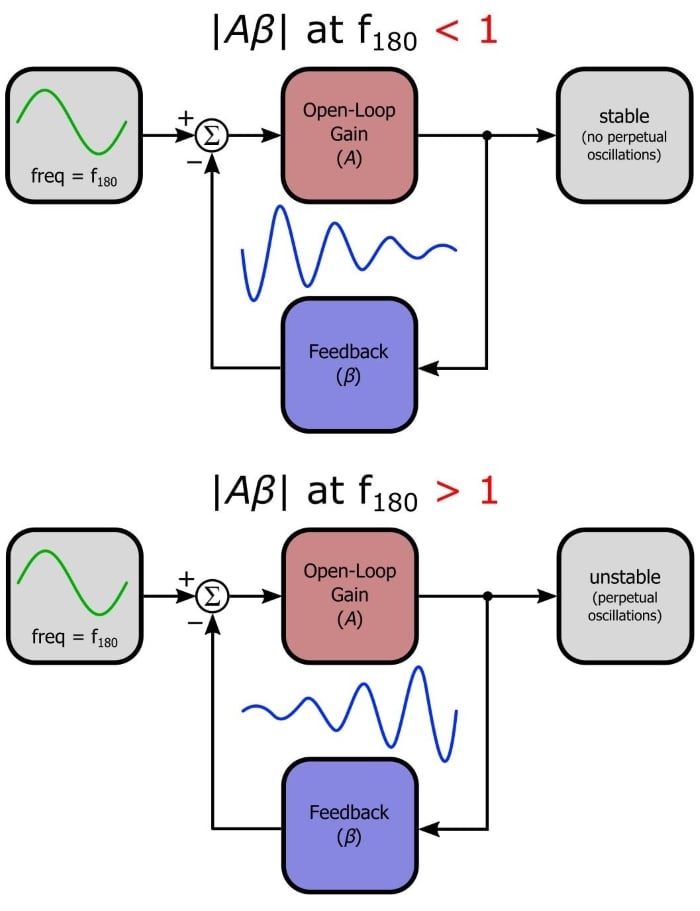
But what if we want an oscillator rather than an amplifier? Well, it is theoretically possible to create an amplifier that has perfectly marginal stability, such that the output will exhibit sustained oscillations. But this can’t work in real life, because something in the circuit or the external environment will change slightly and “tip the balance,” resulting in oscillations that either diminish toward zero or increase toward saturation. A limiter can be used to overcome this serious impediment to designing a reliable oscillator: the initial balance is intentionally tipped in favor of the increase-toward-saturation scenario, but the limiter reduces the loop gain as amplitude increases, resulting in stable oscillation.
The Circuit
Here it is:
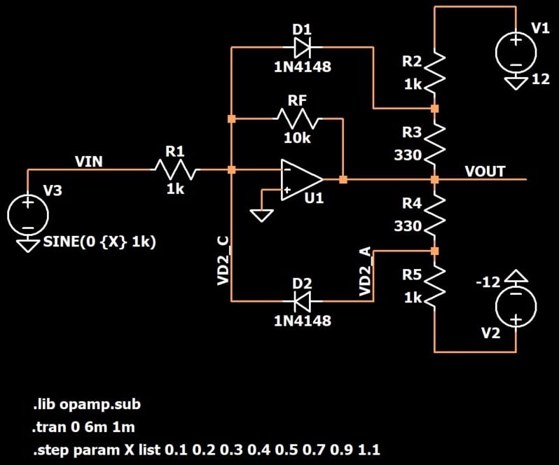
First let’s look at how the circuit works. We’ll just cover the basic concepts here; you can explore the functionality in greater detail via simulations. The nonlinear amplitude control is achieved (not surprisingly) by incorporating the nonlinear current–voltage characteristics of a diode. When the output voltage is low, both diodes are reverse-biased. This means that we can analyze the circuit as if they aren’t even there, and when we do that, we see that the limiter is just a typical inverting op-amp with some resistors connected between the output and the supply voltages. As expected, then, the limiter is just a normal amplifier as long as the output is not high or low enough to provoke its limiting functionality.
As the output increases, though, the voltage at the anode of D2 starts to increase relative to the voltage at the op-amp’s inverting input terminal. Eventually the voltage across the diode will reach ~0.6 V, and the diode will begin to conduct. With D2 conducting, RF is bypassed and the op-amp becomes a voltage follower—in other words, the gain is reduced and the output amplitude is limited. This behavior is shown in the following plot.
The input voltage is decreasing, and consequently the output voltage is increasing. The voltage at the anode of D2 is also increasing, and when the input voltage reaches about –0.4 V, the voltage across D2 is high enough to make the diode start conducting. The voltage across D2 then levels out, as we would expect from a forward-biased diode. The next plot confirms that the output voltage also levels out.
An analogous process occurs with diode D1.
Design Details
The non-limiting gain is set using RF and R1; as you can see in the schematic above, my circuit is set for a non-limiting gain of 10. The next task is establishing the positive and negative voltage limits. If you ponder the circuit for a few minutes you will see that R4 and R5 form a voltage divider, such that the D2 anode voltage (and by extension the positive limit voltage) will depend on the ratio of R4 to R5. Similarly, the D1 cathode voltage (and by extension the negative limit voltage) depends on the ratio of R3 to R2. The full equations (courtesy of Microelectronic Circuits) are as follows:
I calculated resistor values for limits of +5 V and –5 V. The following plot shows that the circuit works as expected; the different traces are the output signals for input-signal amplitudes ranging from 0.1 V to 1.1 V. I really appreciate those smooth transitions from the linear behavior to the limiting behavior.
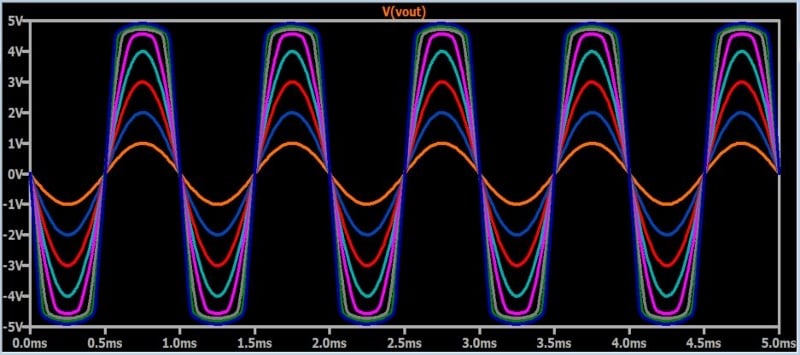
Conclusion
We discussed the applications and functionality of a straightforward op-amp-based limiter, and we looked at a simple design example. If you want to explore this circuit further or experiment with your own design,
Smaller, Self-Healing Transistors Being Developed for Chip-Sized Spacecraft
Spacecraft the size of chips may be the future of space exploration.
Famous cosmologist Stephen Hawking, and physicist/venture capitalist Yuri Milner, announced earlier this year plans to send a fleet of chip-sized spacecraft to Alpha Centauri—our nearest star system neighbor. Currently, the Korea Institute of Science and Technology (KAIST) is exploring methods to overcome some of the impending challenges the harsh interstellar environment will pose to spacecraft on their journey.
Spacecraft the Size of Chips
Breakthrough Starshot is an ambitious project proposing an unusual mode of travel. It is theorized that a chip-sized spacecraft fleet will be capable of travelling up to one-fifth the speed of light, making the 4.37 light-year journey within 30 years.
It is proposed that this fleet will be deployed from space, with ground-based lasers locking onto the individual spacecraft to give them an initial acceleration boost. This light-based propulsion is similar to how solar sails operate; momentum from photons are used to transfer energy, gradually generating speed.

Concept image of the Breakthrough Starshot project. Image courtesy of Breakthrough Initiatives.
Equipped with various sensors, the chips will be able to collect and send data back to Earth. A fly-by of Proxima Centauri b, an exoplanet roughly the same size as Earth and within the habitable zone of its host-star, will provide unprecedented data about our celestial neighbor.
On-Chip Healing
There's obviously no room for maintenance workers on chip-sized spacecraft. Thus, on-chip healing is imperative. The concept of on-chip healing has been around since the 90s, first explored by a microelectronics group in Ireland. KAIST, in particular, is exploring the application of a “gate-all-around” transistor in lieu of the common “fin” transistor layout currently used.
The gate-all-around transistor uses nanoscale wires as channels for the transistor, with the gate surrounding the wire. This wire-gate contact enables current to be passed through, generating heat that would “self-heal” any defects.
Gate-All-Around Transistor. Image courtesy of ExtremeTech.
This gate-all-around layout has the additional benefit of being considerably smaller and lighter than traditional transistors, perfect for chip-sized spacecraft. It is expected that gate-all-around transistors will be able to accommodate gate lengths as small as 5nm by 2020.
It has been reported that KAIST has successfully used gate-all-around transistors to create a microprocessor, DRAM, and flash memory. In their experiments, recovery from damage has been successful up to 10,000 in the flash memory, and 10^12 times in the DRAM. With such results, it is suggested that the chips could regularly self-heal by shutting down and heating its components before powering back up to continue its operations.

A chip with self-healing transistors. Image courtesy of Yang-Kyu Choi of KAIST's Nano-Oriented Bio-Electronics Lab.
In addition to the gate-all-around transistors, KAIST is also researching the application of junction less transistors, similarly using heat to self heal its channels.
NASA is also exploring on-chip self-healing using micro heaters.
While research on self-healing transistors is currently targeting electronics making long-haul space journeys, the results will have positive impacts on everyday electronics too. The chip sized platform challenges engineers and researchers to continue to find ways to miniaturize transistors, which is a fantastic spin-off benefit. As well, self-healing electronics will benefit more local space missions.
One-Nanometer Transistor Keeps Moore’s Law Relevant Another Year
Researchers at the Department of Energy's Lawrence Berkeley National Laboratory have created the world's first one-nanometer transistor gate.
It's no secret that modern research has been vested into reducing the size of electronic components. But how small these new transistors are may even shock industry researchers.
Our modern world of electronics has been achieved due to one remarkable trend: the constant quest to reduce the size of metal oxide semiconductor field effect transistors—MOSFETs.
This component is what is used to amplify and switch electronic signals and is essentially the foundation of most integrated circuits. In the last fifty years, MOSFETs have shrunk down from a few micrometers in size to just 20 nanometers, nearly a thousand-fold smaller.
Unfortunately, conventional silicon electronics have been approaching a fundamental limit to their size. This is due to quantum effects that occur as silicon approaches a gate length of five nanometers, causing unpredictable behavior that significantly inhibits their ability to function reliably. This effect is known as quantum tunneling, where an electron is capable of passing through barriers and is increasingly likely to do so as the barrier size gets smaller.
Companies such as Intel have announced that their intention to research alternative materials to replace silicon once 7nm-length gates were achieved last year. They've now been succeeded by DOE researchers.

A visualization of quantum tunneling. Image courtesy of IEEE Spectrum.
Developing the World's Smallest Transistor Gate
Earlier this month, a research team led by Ali Javey at Lawrence Berkeley National Laboratory created the first working transistor with a one-nanometer gate. The breakthrough was accomplished when the team created a two-dimensional MOSFET using a material called molybdenum disulfide (an alternative to silicon) and a single-walled carbon nanotube as a gate instead of assorted metals. Carbon nanotubes have been the subject of intensive research for years now and recently outperformed silicon in transistors.
The material, MoS2—which has found use in multiple applications across the industry—has quite handily offered a solution to the problem that silicon has with its fundamental limitations. Electrons in MoS2 molecules will act as if they are heavier than those in silicon molecules. This causes the electrons to move more slowly which, in turn, makes them much easier to control.
A representation of the molybdenum disulfide channel and 1-nanometer carbon nanotube gate. Image credit: Sujay Desai/UC Berkeley
Silicon is actually preferable to MoS2 as a channel material in most cases where the electrons will encounter less resistance as they pass through the material. But miniaturizing past the 5nm point with silicon inhibits the gate from preventing electrons that will pass through to the drain, preventing the transistor from switching to off.
The gate was reconstructed using carbon nanotubes due to a reevaluation of materials. Knowing that traditional lithography approaches were not applicable at this scale, the research team instead looked to use carbon nanotubes.
The team was able to measure a device and showed that the new 1nm-thick transistor was capable of controlling electron flow. Including the wiring, the entire device is larger than 1nm and the circuit is altogether functional.
A Realistic View of Nano-Sized Transistors
Amidst the hype of creating the world’s first functioning 1nm gate, the researchers have advised people not to get overly eager to see the new transistor anytime soon.
The paper's lead author, Ali Javey, describes this 1nm gate as "a proof of concept." The process of creating the gate will need to be repeated many, many times before it can even be truly optimized for efficiency. After that point, it will need to be developed further and attached to chips. All of this will likely take years.
In the meantime, however, this step is extraordinarily important because it breaks the five-nanometer limit that silicon places upon transistors.
example power electronics component :
It's been a busy year for mergers and acquisitions in the semiconductor industry. In a market that changes so quickly, companies have realized that the only way to stay afloat is to combine forces. Evolution, it seems, is survival. Here's a look back at some of the largest mergers and acquisitions that have happened so far in 2015:
January
Vishay Intertechnology Inc completes acquisition of Capella Microsystems - Vishay, one of the world's largest manufacturers of discrete semiconductors and passive electronic components, completed its acquisition of Taiwan-based Capella Microsystems Inc., for $205 million. Capella is a fabless IC design company specializing in optoelectronic products.
February
Avago Technologies begins to acquire Emulex Corporation - The $606 million deal will bring a combination of Emulex's connectivity solutions with Avago's Server Storage Connectivity and Fiber Optic products, creating one of the industry's broadest portfolios for Enterprise Storage. "Emulex's connectivity business fits very well with Avago's existing portfolio serving the enterprise storage end market," stated Hock Tan, President and Chief Executive Officer of Avago.
NXP Semiconductors NV completes Quintic acquisition - The industry giant NXP--which posted a revenue of $4.82 billion in 2013--acquired Quintic's assets and IP related to its Wearable and Bluetooth Low Energy business. "With NXP’s strength in ultra-low power microcontrollers and security, broad IoT application solutions offering, and global sales and distribution reach, the acquired Quintic business should become a true leader in its market," said Mark Hamersma, General Manager and SVP Emerging Businesses at NXP.
Arrow Electronics acquires ATM Electronic Corp - Arrow Electronics, a global provider of products, services, and solutions to industrial and commercial users of electronic components and enterprise computing solutions, bought ATM, a leading electronic component distributor based in Taiwan with substantial operations in China. The acquisition will bolster Arrow’s embedded processor, power management, and passive, electromechanical, and connector (PEMCO) product offerings in Asia.
Silicon Laboratories Inc Acquires Bluegiga - Based out of Espoo, Finland, Bluegiga is one of the fastest growing independent providers of short-range wireless connectivity solutions and software for the IoT, so it would make sense for Silicon Laboratories--provider of microcontroller, wireless connectivity, analog and sensor solutions--to incorporate it as part of their IoT strategy. Tyson Tuttle, CEO of Silicon Labs said, “Bluegiga’s wireless modules and software stacks round out our wireless portfolio and complement our IoT solutions. The addition of Bluegiga wireless modules gives us new ways to deliver simplicity to our customers, enabling developers to easily add wireless connectivity to their designs.”
March
NXP acquires Freescale - It what may be the most talked-about acquisition of the year, NXP announced a $40 billion merger to help secure NXP's mission to be the leader in “Secure Connections for a Smarter World.” The merger made NXP the top automotive semiconductor supplier and general-purpose MCU supplier in the world. It also created a high performance mixed signal semiconductor industry leader, with combined revenue of greater than $10 billion. "The combination of NXP and Freescale creates an industry powerhouse focused on the high growth opportunities in the Smarter World. We fully expect to continue to significantly out-grow the overall market, drive world-class profitability and generate even more cash, which taken together will maximize value for both Freescale and NXP shareholders,” said Richard Clemmer, NXP Chief Executive Officer.
Consortium acquires Integrated Silicon Solution, Inc - ISSI is a fabless semiconductor company that designs and markets high performance integrated circuits for the automotive, industrial, medical, networking, mobile communications, and digital consumer electronics markets.
NXP Semiconductors NV acquires Athena SCS - In another move to establish itself securely in the IoT movement, NXP acquired Athena SCS, a provider of solutions securing the rapidly expanding connected world. Athena SCS Ltd. is an independent UK-based developer of state-of-the-art smart card solutions for access, enterprise, eGovernment, transportation, payment and mobile solutions
Lattice Semiconductor closes acquisition of Silicon Image - Lattice Semiconductor, a leading provider of programmable connectivity solutions, closed its acquisition of Silicon Image, Inc., a leading provider of wired and wireless connectivity solutions. Of the merger, Darin G. Billerbeck, Lattice Semiconductor’s President and Chief Executive Officer, said, "...We have significantly expanded our Company’s capabilities, with the addition of MHL, HDMI and 60 GHz Intellectual Property, enhanced our business prospects and financial profile, and further diversified our global customer base."
April
Microsemi completes acquisition of Vitesse - Microsemi, a leading provider of semiconductor solutions differentiated by power, security, reliability and performance, made the move to acquire Vitesse, which designs a diverse portfolio of high-performance semiconductors, application software, and integrated turnkey systems solutions for carrier, enterprise and Internet of Things (IoT) networks worldwide. "This acquisition is further evidence of Microsemi's continuing commitment to grow as a communications semiconductor company," stated James J. Peterson, Microsemi chairman and CEO.
Silicon Motion acquires Shannon Systems - The $57.5 million acquisition joins Silicon Motion, a global leader in NAND flash controllers for solid state storage devices, with a leading supplier of enterprise-class PCIe SSD and storage array solutions to China's internet and other industries. In 2014, Shannon launched the industry's first 6.4TB PCIe SSD with ultra-low access latency and a power envelope of less than 25 watts. More recently, Shannon introduced PCIe-RAIDTM technology, an innovative flash array solution that offers enterprise customers uncompromised performance and high availability.
Nova completes the acquisition of ReVera - Nova, a leading innovator and a key provider of optical metrology solutions for advanced process control used in semiconductor manufacturing, bought ReVera, a leading provider of materials metrology solutions for advanced semiconductor manufacturing for $46.5 million.
May
Avago acquires Broadcom - In another massive acquisition, the chip manufacturer Avago acquired Broadcom, an American fabless semiconductor company in the wireless and broadband communication business, for $37 billion. This puts Avago in the top ranks of semiconductor makers, though still behind Intel and Qualcomm. Avago has been aggressively acquiring companies since it went public in 2009.
Microchip acquires Micrel - The $839 million marries Arizona-based Microchip with the analog semiconductor company Micrel. "Micrel's portfolio of linear and power management products, LAN solutions and timing and communications products, as well as their strong position in the industrial, automotive and communications markets, complement many of Microchip's initiatives in these areas," said Steve Sanghi, president and CEO of Microchip Technology.
June
Intel buys Altera - Altera, a maker of programmable logic semiconductors, was bought by the industry giant for $16.7 billion. In their statement to the public, Intel said, “The acquisition will couple Intel’s leading-edge products and manufacturing process with Altera’s leading field-programmable gate array (FPGA) technology. The combination is expected to enable new classes of products that meet customer needs in the data center and Internet of Things market segments.”
August
Qualcomm acquires Cambridge Silicon Radio Limited - The San Diego-based semiconductor and wireless solutions company Qualcomm completed its acquisition of CSR, a British company specializing in end-to-end semiconductor and software solutions for the Internet of Everything (IoE) and automotive segments.
Power electronics such as voltage regulators, converters and voltage transformers to adapt voltage and current in line with the requirements of your vehicles and systems.

Power electronics, such as transformers and converters, adapt electrical current or electrical voltage from different sources in line with specific consumers, for example to supply power to on-board systems and electronic systems or to operate electric motors and drives.
Opt for transformers and converters either as subsystems or as stand-alone components: We offer both adjustable, standardized units as well as individual systems tailored to meet your requirements. Our transformers and converters operate with a high level of efficiency and reliability.
Our voltage regulators can be used to stabilize an operating voltage to a predefined setpoint value. The various types of bidirectional converters convert direct current into alternating current, and vice versa, while unidirectional inverters generate AC voltage from DC voltage. Voltage transformers vary the voltage level of direct current.
it is a voltage regulator, converter, inverter or voltage transformer, you can rely on our expertise in the field of power electronics.
XXX . XXX 4 zero Switching Regulator Basics: PWM & PFM
As fundamentals of switching regulators, in this section, we describe the voltage control methods. The function of a voltage regulator, irrespective of the type of switching regulator employed, is to generate regulated output voltages. To this end, loop control is performed by feeding the output voltage back to the control circuit, as was explained in the section on “Feedback Control Method”. The subject of this section is voltage control methods, describing what controls are performed in order to adjust the input voltage to, say, 5V.
The switching regulator, as the name implies, converts an input voltage to a desired output voltage by switching the input voltage, that is, by turning it on and off. As was explained in the section on “Operating Principles,” in simple terms this method involves chopping the input voltage and smoothing it out to match the required output voltage. There are two principal methods by which the input voltage is chopped, as described below.
・PWM control (Pulse Width Modulation)
PWM represents the most commonly employed voltage control method. In this method, at fixed cycles the amount of power corresponding to the power that needs to be output is switched on to extract it from the input. Consequently, the ratio between on and off, that is, the duty cycle, changes as a function of the required output electric power.
An advantage of PWM control is that because the frequency is fixed, any switching noise that arises can be predicted, thus facilitating the filtering process. A drawback of the method is that also due to constant frequency, the number of switching operations remains the same whether the load is high or low, and consequently, the self-consuming current does not change. As a result, at times of light loads the switching loss becomes predominant, which reduces the efficiency significantly.

● The frequency is constant, and output voltage is adjusted with duty cycle
- The fixed frequency facilitates the noise filtering
- Because the frequency remains fixed even during light-load operations, switching loss reduces the efficiency
・PFM control (Pulse Frequency Modulation)
PFM is of two types: the fixed-on time type and the fixed-off time type. In the case of the fixed-on time type as an example (see the figure below), on-time is fixed with variable off-time. In other words, the length of time it takes for the power to turn on next time varies. When the load increases, the number of on-times in a given length of time is increased to keep pace with the load. Thus, under a heavy load, the frequency increases, and under a light load it diminishes.
PFM is of two types: the fixed-on time type and the fixed-off time type. In the case of the fixed-on time type as an example (see the figure below), on-time is fixed with variable off-time. In other words, the length of time it takes for the power to turn on next time varies. When the load increases, the number of on-times in a given length of time is increased to keep pace with the load. Thus, under a heavy load, the frequency increases, and under a light load it diminishes.
On the positive side, because not a great deal of power needs to be added during a light-load operation, the switching frequency is reduced, and the number of required switching operations decreases, with reduces switching losses. As a consequence, the PFM method ensures that high efficiency is maintained even at a light load. On the negative side, because the frequency varies, the noise associated with the switching remains indefinite, making the filtering process difficult to control and the noise difficult to remove. Also, if noise enters below 20 kHz, which is an audible band, the problem of ringing can occur, which produces an adverse impact on S/N in audio devices. As far as noise is concerned, PWM may be preferable in many respects.

● On- (or off-) time is fixed, and off- (or on-) time is adjusted
- Reduced-frequency operations at a light load cut switching loss and maintain efficiency.
- The unknown frequency makes noise-filtering difficult, with the result that some noise ends up in an audible band
The question of which method, PWM vs. PFM, is to be adopted requires a good understanding of the properties of the two methods, and involves trade-offs. To achieve the best of the two worlds and maintain high efficiency, there are ICs that operate in PWM during steady-state operations and that switch to PFM to handle light loads.

● Efficiency characteristics of PWM and PFM illustrated
- PWM, switching at fixed cycles even during a light load, can be low in efficiency.
- PFM, which operates by reducing the frequency under a light load, cuts switching losses and maintain a high efficiency.
- There are types of ICs that act in PWM during steady-state operations and that switch to PFM during a light-load, for reduced noise and improved efficiency during a light-load.
Key Points:
・In pulse-width modulation (PWM), the frequency is constant, and duty cycle is used to control the voltage.
・ PFM (pulse frequency modulation) operates with a fixed pulse on-time (or off-time) and performs control by varying the off-time (or on-time).
・ These methods should be used with a good understanding of their positive and negative aspects.
・ There has been a slew of ICs that are designed to switch between the two types of controls and incorporate even finer control modes.
The Advantages of Pulse Frequency Modulation for DC/DC Switching Voltage Converters
The popularity of DC/DC switching voltage converters primarily derives from their efficient regulation over a wide range of voltage inputs and output current compared with linear regulators. However, at lower loads, efficiency tails off as the quiescent current of the converter IC itself becomes the significant contributor to system losses.
Leading power component manufacturers now offer a range of “dual-mode” switching converters that automatically shift from the popular pulse width modulation (PWM) regulation method to a pulse frequency modulation (PFM) technique at a preset current threshold in order to improve efficiency under low loads.
This article describes how PFM works, explains its benefits and some of its disadvantages, and then considers how some silicon vendors implement the technique in their integrated power chips.
PWM vs. PFM
PWM is not the only technique for regulating the output of a switching converter. Instead of modifying the duty cycle of a fixed-frequency square wave to regulate the output of a power supply, it is also possible to use a constant duty cycle and then modulate the square wave’s frequency (PFM) to achieve regulation. DC/DC voltage converters equipped with constant-on-time or constant-off-time control are typical examples of PFM architecture.
A second example of a PFM architecture is a so-called hysteretic voltage converter that uses a simple method for regulation whereby the MOSFET is turned on and off based on the output-voltage changes sensed by the converter. This architecture is sometimes referred to as a “ripple regulator” or “bang-bang controller” because it continuously shuttles the output voltage back and forth to just above or below the set point. Hysteresis is used to maintain predictable operation and to avoid switch chatter. Because the hysteretic architecture varies the drive signal to the MOSFETs based on the operating conditions of the circuit, the switching frequency varies.
PFM architectures do offer some advantages for DC/DC conversion, including better low-power conversion efficiency, lower total solution cost, and simple converter topologies that do not require control-loop-compensation networks, but are less popular than PWM devices due to some notable drawbacks.
The first is the control of EMI. Filtering circuits for a fixed-frequency switching converter are much easier to design than those for a device that operates across a wide range of frequencies. Second, PFM architectures tend to lead to greater voltage ripple at the output that can cause problems for the sensitive silicon being supplied. Third, PFM operation at low (or even zero) frequency increases the transient response time of the switching converter that could lead to slow response and consumer disappointment in some portable applications.
However, by combining the merits of a PWM architecture with those of a PFM device in a monolithic “dual-mode” switching converter, manufacturers can offer a solution with high efficiency across its entire operating range. The EMI concerns associated with PFM are mitigated to a great extent because the root cause of such interference is fast switching at high currents and high voltages, whereas in dual-mode chips, variable-frequency operation is only used during low-current and low-voltage operation.
Energy losses in a switching voltage regulator
The most common technique for regulating the voltage of a switching device is to use an oscillator and PWM controller to produce a rectangular pulse wave that toggles the unit’s internal MOSFET (or MOSFETs in a synchronous device) at a set frequency typically in the hundreds of megahertz range. (Higher frequencies allow smaller magnetic components at the expense of greater electromagnetic interference [EMI] challenges.) The output voltage of the regulator is proportional to the duty cycle of the PWM waveform.
Generally the technique works well, but at low loads efficiency is compromised. To understand why, it pays to consider where losses, energy drawn at the voltage regulator’s input that is not transferred to the output load, occur.
There are four main sources of loss in a switching regulator. The first is the dynamic loss due to the energy used to charge and discharge the MOSFET gate capacitance, and is highest when the transistor(s) operate at high frequency. These switching losses occur when current flows through the drain-source channel while there is significant differential voltage across it. Other MOSFET losses occur when passing high currents through the nonzero channel resistance of the power-switching elements. (This is why power component manufacturers work so hard to reduce the “on-resistance” of their products.)
In addition to the switching components, the passive devices in the switching regulator’s circuitry are also prone to inefficiencies. For the inductor, the losses result from conduction (in the windings) and magnetic core. For capacitors, the losses are typically associated with the equivalent series resistance (ESR) of the component and are determined by the capacitance of the device, its operating frequency, and its load current.
There are two ways to implement a switching regulator. An engineer can either construct a device from scratch using discrete components or they can base the power supply on one of many converter ICs available from major semiconductor vendors such as Texas Instruments, Linear Technology, and Fairchild Semiconductor. The advantage of a module is that the design process is simplified. (See the TechZone article “DC/DC Voltage Regulators: How to Choose Between Discrete and Modular Design.”)
However, the converter IC itself contributes to the overall loss of the switching regulator. For example, some energy is needed to provide internal bias currents for amplifiers, comparators, and references, but the dominant losses for the IC are associated with the internal oscillator and drive circuits for the PWM controller. Such losses are relatively insignificant when the switching regulator is subject to high load, but as the load decreases, the losses associated with switching and external passive devices decrease while those associated with the converter IC remain constant.
That presents something of a dilemma for the designer of a portable product. The engineer is under pressure to manage the battery budget, so the choice of an efficient switching regulator (compared to, for example, a linear regulator) seems the obvious choice. (See the TechZone article “Design Techniques for Extending Li-Ion Battery Life.”) However, portable products spend considerable periods under low-power “standby” or “sleep” modes, where the demand on the switching converter is modest and it is operating relatively inefficiently.
A typical handheld device may draw around an amp when fully operational but demand less than one milliamp when in standby or sleep mode. Considering that the converter IC itself can consume up to a few milliamps simply to preserve its operational status, it is little surprise that the conversion efficiency is poor under low-load conditions because the regulator’s quiescent current represents a significant fraction of the total load.
Improving efficiency
To address the dominant losses (that is, those associated with the internal oscillator and drive circuits for the PWM controller) a designer can select one of many dual-mode switching converters on the market. The devices combine normal PWM operation with a PFM technique (that typically features variable frequencies typically much lower than the normal fixed frequency when operating under PWM).
When a dual-mode switching converter operates at moderate to high currents, it runs in continuous-conduction mode (whereby the current in the inductor never falls to zero). As the load current decreases, the converter may switch to discontinuous mode (when the current in the inductor does fall to zero due to the light load). At very light loads, the converter goes into PFM (sometimes referred to as “Power Saving Mode” [PSM] by manufacturers). Other vendors take variable-frequency operation to an extreme by stopping the oscillator altogether (often referred to as “pulse skipping”).
It should be noted that the use of PFM at low loads does not mean the switching converter uses a PFM architecture, rather, it employs an PWM architecture that is able to utilize PFM operation as required.
Under light-load conditions, a switching converter’s output capacitor can maintain the output voltage for some period of time between switching pulses. In the ideal case, the oscillator could be turned completely off at a no-load condition and the output voltage would remain constant due to the charged state of the output capacitor. However, parasitic losses drain the capacitor and the circuit requires at least occasional pulsing of the power switches to maintain the regulated output voltage in regulation.
During PFM operation the output power is proportional to the average frequency of the pulse train, and the converter operates when the output voltage drops below the set output voltage as measured by the feedback control loop. The frequency of converter switching is then increased until the output voltage reaches a typical value between the set output voltage and 0.8 to 1.5 percent above the set output voltage (Figure 1 illustrates the technique).

Figure 1: PFM varies the frequency of a rectangular pulse train of fixed duty cycle to meet load demand.
Side effects of PFM operation
An increase in voltage output ripple is often observed when the switching converter flips to PFM mode because of the need for a tolerance band (rather than a fixed point) to sense when the power switches need to be turned on again. If a narrower tolerance band is used, the converter switches more frequently, which reduces the power saving. The engineer must decide on the best trade-off between improved low-load efficiency and increased voltage output ripple. Figures 2a and 2b illustrate the difference in voltage ripple for a switching converter operating in PWM and PFM modes, respectively.

Figure 2: Voltage ripple for PWM mode (a) and PFM operation (b) (Courtesy of Analog Devices).
During load transients, any switching converter will exhibit some amount of overshoot during a high-to-low-load transient or undershoot during a low-to-high-load transient. In the case of a converter that is operating in a PSM, the load level is already low, so the next transient will be from low-to-high current (which typically corresponds to transitioning from sleep to active mode). The increased load on the regulator output often results in “output-voltage sag” until the converter loop has time to respond.
Some switching converters include provision to minimize this voltage sag. TI’s TPS62400 employs “dynamic voltage positioning”. During PSM operation, the output-voltage set point is increased slightly (for example, by 1 percent) to anticipate the instantaneous voltage-sagging transient that occurs when the load is suddenly stepped higher. This prevents the output voltage from falling below its desired window of regulation during the initial load transient.
Some devices also offer an enhancement that can be used to balance the compromise between good transient response (best in PWM mode) and low power consumption (best in PSM). The enhancement is an intermediate mode that the engineer can implement using I²C commands to the converter IC that offers better transient response than PSM, but is more efficient than PWM. The intermediate mode is a good option for a system that goes from a high load to a very light load (for example, sleep mode).
PFM in commercial chips
PFM operation at low loads can reduce the quiescent current of the IC from several mA down to a few μA. Figure 3 shows the power-conversion efficiency of the TPS62400 switching converter when it is operating in PWM mode compared to PSM at light-load levels.

Figure 3: Efficiency improvements when implementing PSM for TI TPS62400.
From Figure 3 it can be seen that while PWM mode maintains good efficiency above 100 mA, the use of PSM boosts efficiency to between 80 and 90 percent even at load currents below 1 mA. If the converter operated in PWM mode during such light loads, its operating current would be significantly higher than the load current, resulting in very-poor conversion efficiency (well under 30 percent).
Analog Devices offers several switching converters with PSM. When this mode is entered, an offset induced in the PWM regulation level causes the output voltage to rise, until it reaches approximately 1.5 percent above the PWM regulation level, at which point PWM operation turns off: both power switches are off, and idle mode is entered. The output capacitor is allowed to discharge until VOUT falls to the PWM regulation voltage. The device then drives the inductor, causing VOUT to again rise to the upper threshold. This process is repeated as long as the load current is below the PSM current threshold.
The company’s ADP2108 voltage regulator employs PSM to improve efficiency from 40 to 75 percent with an input voltage of 2.3 V and an output current of 10 mA. The chip is a 3 MHz step-down (‘buck’) converter offering 3.3 V output from 2.3 to 5.5 V input at up to 600 mA. Figure 4 shows the point at which the PWM to PSM transition occurs.

Figure 4: PWM to PSM threshold for Analog Devices’ ADP2108.
Other power component manufacturers also offer dual-mode switching converters. Linear Technology supplies the LTC3412A, which features both “Burst Mode” and pulse-skipping operation to improve efficiency at low loads. The chip is a buck converter that can operate across an input range of 2.25 to 5.5 V providing an output of 0.8 to 5 V at up to 3 A.
Burst Mode is an example of the intermediate PFM technique described above that improves efficiency while maintaining reasonable transient response. For example, by implementing Burst Mode, the efficiency at 10 mA output current (VIN 3.3 V, VOUT 2.5 V) is improved from 30 to 90 percent. The LTC3412A also includes a conventional pulse-skipping operational mode that further reduces switching losses at low loads.
Extending battery life
PWM-controlled switching converters are the popular choice when a design engineer needs to extend battery life in a portable product. However, it’s important to remember that many portable products spend a lot of time in low-power sleep modes just at the point of operation where the converter is at its least efficient. Although the demand on the battery is modest, over the long term the current adds up and battery life is compromised.
By employing a converter that uses a PWM architecture but that benefits from PFM or other PSM techniques below a certain load threshold, the designer can benefit from the advantages of PWM during normal operation, but preserve battery capacity during the extended periods when many portable devices sit idle.
Leading power component manufacturers now offer a range of “dual-mode” switching converters that automatically shift from the popular pulse width modulation (PWM) regulation method to a pulse frequency modulation (PFM) technique at a preset current threshold in order to improve efficiency under low loads.
This article describes how PFM works, explains its benefits and some of its disadvantages, and then considers how some silicon vendors implement the technique in their integrated power chips.
PWM vs. PFM
PWM is not the only technique for regulating the output of a switching converter. Instead of modifying the duty cycle of a fixed-frequency square wave to regulate the output of a power supply, it is also possible to use a constant duty cycle and then modulate the square wave’s frequency (PFM) to achieve regulation. DC/DC voltage converters equipped with constant-on-time or constant-off-time control are typical examples of PFM architecture.
A second example of a PFM architecture is a so-called hysteretic voltage converter that uses a simple method for regulation whereby the MOSFET is turned on and off based on the output-voltage changes sensed by the converter. This architecture is sometimes referred to as a “ripple regulator” or “bang-bang controller” because it continuously shuttles the output voltage back and forth to just above or below the set point. Hysteresis is used to maintain predictable operation and to avoid switch chatter. Because the hysteretic architecture varies the drive signal to the MOSFETs based on the operating conditions of the circuit, the switching frequency varies.
PFM architectures do offer some advantages for DC/DC conversion, including better low-power conversion efficiency, lower total solution cost, and simple converter topologies that do not require control-loop-compensation networks, but are less popular than PWM devices due to some notable drawbacks.
The first is the control of EMI. Filtering circuits for a fixed-frequency switching converter are much easier to design than those for a device that operates across a wide range of frequencies. Second, PFM architectures tend to lead to greater voltage ripple at the output that can cause problems for the sensitive silicon being supplied. Third, PFM operation at low (or even zero) frequency increases the transient response time of the switching converter that could lead to slow response and consumer disappointment in some portable applications.
However, by combining the merits of a PWM architecture with those of a PFM device in a monolithic “dual-mode” switching converter, manufacturers can offer a solution with high efficiency across its entire operating range. The EMI concerns associated with PFM are mitigated to a great extent because the root cause of such interference is fast switching at high currents and high voltages, whereas in dual-mode chips, variable-frequency operation is only used during low-current and low-voltage operation.
Energy losses in a switching voltage regulator
The most common technique for regulating the voltage of a switching device is to use an oscillator and PWM controller to produce a rectangular pulse wave that toggles the unit’s internal MOSFET (or MOSFETs in a synchronous device) at a set frequency typically in the hundreds of megahertz range. (Higher frequencies allow smaller magnetic components at the expense of greater electromagnetic interference [EMI] challenges.) The output voltage of the regulator is proportional to the duty cycle of the PWM waveform.
Generally the technique works well, but at low loads efficiency is compromised. To understand why, it pays to consider where losses, energy drawn at the voltage regulator’s input that is not transferred to the output load, occur.
There are four main sources of loss in a switching regulator. The first is the dynamic loss due to the energy used to charge and discharge the MOSFET gate capacitance, and is highest when the transistor(s) operate at high frequency. These switching losses occur when current flows through the drain-source channel while there is significant differential voltage across it. Other MOSFET losses occur when passing high currents through the nonzero channel resistance of the power-switching elements. (This is why power component manufacturers work so hard to reduce the “on-resistance” of their products.)
In addition to the switching components, the passive devices in the switching regulator’s circuitry are also prone to inefficiencies. For the inductor, the losses result from conduction (in the windings) and magnetic core. For capacitors, the losses are typically associated with the equivalent series resistance (ESR) of the component and are determined by the capacitance of the device, its operating frequency, and its load current.
There are two ways to implement a switching regulator. An engineer can either construct a device from scratch using discrete components or they can base the power supply on one of many converter ICs available from major semiconductor vendors such as Texas Instruments, Linear Technology, and Fairchild Semiconductor. The advantage of a module is that the design process is simplified. (See the TechZone article “DC/DC Voltage Regulators: How to Choose Between Discrete and Modular Design.”)
However, the converter IC itself contributes to the overall loss of the switching regulator. For example, some energy is needed to provide internal bias currents for amplifiers, comparators, and references, but the dominant losses for the IC are associated with the internal oscillator and drive circuits for the PWM controller. Such losses are relatively insignificant when the switching regulator is subject to high load, but as the load decreases, the losses associated with switching and external passive devices decrease while those associated with the converter IC remain constant.
That presents something of a dilemma for the designer of a portable product. The engineer is under pressure to manage the battery budget, so the choice of an efficient switching regulator (compared to, for example, a linear regulator) seems the obvious choice. (See the TechZone article “Design Techniques for Extending Li-Ion Battery Life.”) However, portable products spend considerable periods under low-power “standby” or “sleep” modes, where the demand on the switching converter is modest and it is operating relatively inefficiently.
A typical handheld device may draw around an amp when fully operational but demand less than one milliamp when in standby or sleep mode. Considering that the converter IC itself can consume up to a few milliamps simply to preserve its operational status, it is little surprise that the conversion efficiency is poor under low-load conditions because the regulator’s quiescent current represents a significant fraction of the total load.
Improving efficiency
To address the dominant losses (that is, those associated with the internal oscillator and drive circuits for the PWM controller) a designer can select one of many dual-mode switching converters on the market. The devices combine normal PWM operation with a PFM technique (that typically features variable frequencies typically much lower than the normal fixed frequency when operating under PWM).
When a dual-mode switching converter operates at moderate to high currents, it runs in continuous-conduction mode (whereby the current in the inductor never falls to zero). As the load current decreases, the converter may switch to discontinuous mode (when the current in the inductor does fall to zero due to the light load). At very light loads, the converter goes into PFM (sometimes referred to as “Power Saving Mode” [PSM] by manufacturers). Other vendors take variable-frequency operation to an extreme by stopping the oscillator altogether (often referred to as “pulse skipping”).
It should be noted that the use of PFM at low loads does not mean the switching converter uses a PFM architecture, rather, it employs an PWM architecture that is able to utilize PFM operation as required.
Under light-load conditions, a switching converter’s output capacitor can maintain the output voltage for some period of time between switching pulses. In the ideal case, the oscillator could be turned completely off at a no-load condition and the output voltage would remain constant due to the charged state of the output capacitor. However, parasitic losses drain the capacitor and the circuit requires at least occasional pulsing of the power switches to maintain the regulated output voltage in regulation.
During PFM operation the output power is proportional to the average frequency of the pulse train, and the converter operates when the output voltage drops below the set output voltage as measured by the feedback control loop. The frequency of converter switching is then increased until the output voltage reaches a typical value between the set output voltage and 0.8 to 1.5 percent above the set output voltage (Figure 1 illustrates the technique).
Figure 1: PFM varies the frequency of a rectangular pulse train of fixed duty cycle to meet load demand.
Side effects of PFM operation
An increase in voltage output ripple is often observed when the switching converter flips to PFM mode because of the need for a tolerance band (rather than a fixed point) to sense when the power switches need to be turned on again. If a narrower tolerance band is used, the converter switches more frequently, which reduces the power saving. The engineer must decide on the best trade-off between improved low-load efficiency and increased voltage output ripple. Figures 2a and 2b illustrate the difference in voltage ripple for a switching converter operating in PWM and PFM modes, respectively.
Figure 2: Voltage ripple for PWM mode (a) and PFM operation (b) (Courtesy of Analog Devices).
During load transients, any switching converter will exhibit some amount of overshoot during a high-to-low-load transient or undershoot during a low-to-high-load transient. In the case of a converter that is operating in a PSM, the load level is already low, so the next transient will be from low-to-high current (which typically corresponds to transitioning from sleep to active mode). The increased load on the regulator output often results in “output-voltage sag” until the converter loop has time to respond.
Some switching converters include provision to minimize this voltage sag. TI’s TPS62400 employs “dynamic voltage positioning”. During PSM operation, the output-voltage set point is increased slightly (for example, by 1 percent) to anticipate the instantaneous voltage-sagging transient that occurs when the load is suddenly stepped higher. This prevents the output voltage from falling below its desired window of regulation during the initial load transient.
Some devices also offer an enhancement that can be used to balance the compromise between good transient response (best in PWM mode) and low power consumption (best in PSM). The enhancement is an intermediate mode that the engineer can implement using I²C commands to the converter IC that offers better transient response than PSM, but is more efficient than PWM. The intermediate mode is a good option for a system that goes from a high load to a very light load (for example, sleep mode).
PFM in commercial chips
PFM operation at low loads can reduce the quiescent current of the IC from several mA down to a few μA. Figure 3 shows the power-conversion efficiency of the TPS62400 switching converter when it is operating in PWM mode compared to PSM at light-load levels.
Figure 3: Efficiency improvements when implementing PSM for TI TPS62400.
From Figure 3 it can be seen that while PWM mode maintains good efficiency above 100 mA, the use of PSM boosts efficiency to between 80 and 90 percent even at load currents below 1 mA. If the converter operated in PWM mode during such light loads, its operating current would be significantly higher than the load current, resulting in very-poor conversion efficiency (well under 30 percent).
Analog Devices offers several switching converters with PSM. When this mode is entered, an offset induced in the PWM regulation level causes the output voltage to rise, until it reaches approximately 1.5 percent above the PWM regulation level, at which point PWM operation turns off: both power switches are off, and idle mode is entered. The output capacitor is allowed to discharge until VOUT falls to the PWM regulation voltage. The device then drives the inductor, causing VOUT to again rise to the upper threshold. This process is repeated as long as the load current is below the PSM current threshold.
The company’s ADP2108 voltage regulator employs PSM to improve efficiency from 40 to 75 percent with an input voltage of 2.3 V and an output current of 10 mA. The chip is a 3 MHz step-down (‘buck’) converter offering 3.3 V output from 2.3 to 5.5 V input at up to 600 mA. Figure 4 shows the point at which the PWM to PSM transition occurs.
Figure 4: PWM to PSM threshold for Analog Devices’ ADP2108.
Other power component manufacturers also offer dual-mode switching converters. Linear Technology supplies the LTC3412A, which features both “Burst Mode” and pulse-skipping operation to improve efficiency at low loads. The chip is a buck converter that can operate across an input range of 2.25 to 5.5 V providing an output of 0.8 to 5 V at up to 3 A.
Burst Mode is an example of the intermediate PFM technique described above that improves efficiency while maintaining reasonable transient response. For example, by implementing Burst Mode, the efficiency at 10 mA output current (VIN 3.3 V, VOUT 2.5 V) is improved from 30 to 90 percent. The LTC3412A also includes a conventional pulse-skipping operational mode that further reduces switching losses at low loads.
Extending battery life
PWM-controlled switching converters are the popular choice when a design engineer needs to extend battery life in a portable product. However, it’s important to remember that many portable products spend a lot of time in low-power sleep modes just at the point of operation where the converter is at its least efficient. Although the demand on the battery is modest, over the long term the current adds up and battery life is compromised.
By employing a converter that uses a PWM architecture but that benefits from PFM or other PSM techniques below a certain load threshold, the designer can benefit from the advantages of PWM during normal operation, but preserve battery capacity during the extended periods when many portable devices sit idle.
DCDC Converters (Switching Regulators)
PWM Control and VFM Control
Ricoh’s DCDC converters are pulse-width modulation (PWM) controlled or variable-frequency modulation (VFM) controlled. VFM is also called pulse-frequency modulation (PFM).
PWM Control
The oscillator frequency is constant and the pulse width (ON time) changes according to the amount of output load.

VFM Control
The pulse width (ON time) is constant and the oscillator frequency changes according to the amount of output load.

The features of VFM control and PWM control are as described below.
| Oscillator Frequency | Pulse Width (Duty) | Light Load Condition | Noise Suppression*1 | ||
|---|---|---|---|---|---|
| Efficiency | Ripple Voltage | ||||
| VFM Control | Change | Constant | Good | High | Difficult |
| PWM Control | Constant | Change | Not Good | Low | Easy |
- *1Noise suppression of VFM control can be difficult because oscillator frequency is inconsistent and it affects noise level.
Noise suppression of PWM control is relatively easier because oscillator frequency is constant and it does not affect noise level.
Ricoh’s DCDC converters include the products that are only operated by PWM control and the products that can be automatically switched between PWM mode and VFM mode according to the load condition.
RP506K Efficiency vs. Output Current


Forced PWM Control
The general PWM control DCDC converters may cause ringing in the Lx voltage because there is a zero current period to prevent a reverse coil current in low load condition.
However the forced PWM control DCDC converters do not cause ringing by forcing them into PWM control in low load condition.
Although the reverse coil current is present, the reverse current is not wasted because it flows to the output in the next cycle.
However the forced PWM control DCDC converters do not cause ringing by forcing them into PWM control in low load condition.
Although the reverse coil current is present, the reverse current is not wasted because it flows to the output in the next cycle.
General PWM Control

Forced PWM Control

Ricoh forced PWM control DCDC converters are able to switch automatically between PWM and VFM control.
If one prefers that the supply current and efficiency are most important, please select automatic PWM/VFM switching mode.
If one prefers that the supply current and efficiency are most important, please select automatic PWM/VFM switching mode.
In that case the DCDC converter operates in VFM control during low load conditions.
If one prefers that no ringing in low load condition should appear and operation with a constant frequency, please select fixed forced PWM control.
If one prefers that no ringing in low load condition should appear and operation with a constant frequency, please select fixed forced PWM control.
Voltage- and Current-Mode Control for PWM Signal Generation in DC-to-DC Switching Regulators
Switching DC-to-DC voltage converters (“regulators”) comprise two elements: A controller and a power stage. The power stage incorporates the switching elements and converts the input voltage to the desired output. The controller supervises the switching operation to regulate the output voltage. The two are linked by a feedback loop that compares the actual output voltage with the desired output to derive the error voltage.
The controller is key to the stability and precision of the power supply, and virtually every design uses a pulse-width modulation (PWM) technique for regulation. There are two main methods of generating the PWM signal: Voltage-mode control and current-mode control. Voltage-mode control came first, but its disadvantages––such as slow response to load variations and loop gain that varied with input voltage––encouraged engineers to develop the alternative current-based method.
Today, engineers can select from a wide range of power modules using either control technique. These products incorporate technology to overcome the major deficiencies of the previous generation.
This article describes voltage- and current-mode control technique for PWM-signal generation in switching-voltage regulators and explains where each application is best suited.
Voltage-mode control
Designers tasked with building a power supply can either build a unit from discrete components (see the TechZone article “DC/DC Voltage Regulators: How to Choose Between Discrete and Modular Design”), separate controller and power components, or power supply modules that integrate both elements into a single chip.
But whichever design technique is employed, there is a high probability that regulation will employ a PWM technique of (typically) a fixed frequency. (A constant-switching frequency is desirable because it limits electromagnetic interference (EMI) generated by the power supply.)
In a voltage-mode controlled regulator, the PWM signal is generated by applying a control voltage (VC) to one comparator input and a sawtooth voltage (Vramp) (or “PWM ramp”) of fixed frequency, generated by the clock, to the other (Figure 1).

Figure 1: PWM generator for switching-voltage regulator. (Courtesy: Texas Instruments)
The duty cycle of the PWM signal is proportional to the control voltage and determines the percentage of the time that the switching element conducts and therefore, in turn, the output voltage (see the TechZone article “Using PFM to Improve Switching DC/DC Regulator Efficiency at Low Loads”). The control voltage is derived from the difference between the actual-output voltage and the desired-output voltage (or reference voltage).
The modulator gain Fm is defined as the change in control voltage that causes the duty cycle to go from 0 to 100 percent (Fm = d/VC = 1/Vramp).1
Figure 2 shows the building blocks of a typical switching regulator. The power stage comprises a switch, diode, inductor, transformer (for isolated designs), and input/output capacitors. This stage converts the input voltage (VIN) into the output voltage (VO). The voltage regulator’s control section comprises an error amplifier with the reference voltage (equal to the desired output) on one input and the output from a voltage divider on the other. The voltage divider is fed from a feedback trace from the output. The output from the error amplifier provides the control voltage (VC or “error voltage”) that forms one input to the PWM comparator.2

Figure 2: Control section and power stage of voltage-mode control-switching regulator. (Courtesy of Microsemi)
The advantages of voltage-mode control include: A single-feedback loop making design and circuit analysis easier; the use of a large-amplitude ramp waveform providing good noise margin for a stable-modulation process, and a low-impedance power output providing better cross-regulation for multiple-output supplies.
But the technique also has some notable drawbacks. For example, changes in load must first be sensed as an output change and then corrected by the feedback loop — resulting in slow response. The output filter complicates circuit compensation, which can be made even more difficult due to the fact that the loop gain varies with input voltage.
Current-mode control
In the early 1980s, engineers came up with an alternative-switching-voltage regulator technique that addressed the deficiencies of the voltage-mode control method. Called current-mode control, the technique derives the PWM ramp by adding a second loop feeding back the inductor current. This feedback signal comprises two parts: the AC-ripple current, and the DC or average value of the inductor current. An amplified form of the signal is routed to one input of the PWM comparator while the error voltage forms the other input. As with the voltage-mode control method, the system clock determines the PWM-signal frequency (Figure 3).

Figure 3: Current-mode control-switching regulator. Here the PWM ramp is generated from a signal derived from the output-inductor current. (Courtesy of Texas Instruments)
Current-mode control addresses the slow response of voltage-mode control because the inductor current rises with a slope determined by the difference between the input and output voltages and hence responds immediately to line- or load-voltage changes. A further advantage is that current-mode control eliminates the loop-gain variation with input voltage drawback of the voltage-mode control method.
Furthermore, since in a current-mode control circuit the error amplifier commands an output current rather than voltage, the effect of the output inductor on circuit response is minimized and compensation is made easier. The circuit also exhibits a higher-gain bandwidth compared to a voltage-mode control device.
Additional benefits of current-mode control include inherent pulse-by-pulse current limiting by clamping the command from the error amplifier, and simplified-load sharing when multiple power units are employed in parallel.
For a while, current-mode control looked to have consigned voltage-mode control to history. However, although they took a while to surface, engineers discovered that current-mode control regulators brought their own design challenges.
A major drawback is that circuit analysis is difficult because the topology of the regulator now includes two feedback loops. A second complication is instability of the “inner” control loop (carrying the inductor current signal) at duty cycles above 50 percent. A further challenge comes from the fact that because the control loop is derived from the inductor output current, resonances from the power stage can introduce noise into this inner control loop.3
Limiting a current-mode control regulator to a duty cycles of less than 50 percent imposes serious limitations on the input voltage of the device. Fortunately, the instability problem can be resolved by “injecting” a small amount of slope compensation into the inner loop. This technique ensures stable operation for all values of the PWM duty cycle.
Slope compensation is achieved by subtracting a sawtooth-voltage waveform (running at the clock frequency) from the output of the error amplifier. Alternatively, the compensation-slope voltage can be added directly to the inductor-current signal (Figure 4).

Figure 4: Current-mode control regulator with slope compensation. (Courtesy of Texas Instruments)
Mathematical analysis shows that to guarantee current-loop stability the slope of the compensation ramp must be greater than one-half of the down slope of the current waveform.4
There are many current-mode control regulators commercially available. Microsemi, for example, offers the NX7102 synchronous step-down (“buck”) regulator with current-mode control. The chip can accept an input range of 4.75 to 18 V and offers an adjustable output down to 0.925 V. Maximum output current is 3 A and peak efficiency is between 90 and 95 percent depending on the input voltage.
For its part, Texas Instruments offers a wide range of current-mode control regulators. One example is the TPS63060, a synchronous buck/step-up (“boost”) 2.4 MHz regulator offering an output of 2.5 to 8 V (at up to 1 A) from a 2.5 to 12 V supply. The device offers up to 93 percent efficiency and is targeted at mobile applications, such as portable computers and industrial-metering equipment.
STMicroelectronics also supplies a range of current-mode control devices including the STBB2. This is a synchronous buck/boost 2.5 MHz regulator providing an output of either 2.9 or 3.4 V from a 2.4 to 5.5 V input. The device is able to supply up to 800 mA at 90 percent efficiency and is supplied in a ball-grid array (BGA) package.
The resurgence of voltage-mode
A look through some silicon vendor catalogs reveals that voltage-mode control regulators have not gone away. The reason for this is that the key weaknesses of the previous generation of devices have been addressed by using a technique called voltage feed-forward.
Voltage feed-forward is accomplished by modifying the slope of the PWM ramp waveform with a voltage proportional to the input voltage. This provides a corresponding and correcting duty cycle modulation independent of the feedback loop.
The technique improves circuit response to line and load transients while eliminating sensitivity to the presence of an input filter. Voltage feed-forward also stabilizes the loop gain such that it no longer varies with input voltage. A minor drawback is some added-circuit complexity because a sensor is needed to detect the input voltage.
Engineers are able to select from a wide range of voltage-mode control regulators from the major suppliers. For example, Maxim offers a number of voltage-mode control devices in its portfolio including the MAX5073. This switching regulator is a buck/boost 2.2 MHz device operating from a 5.5 to 23 V supply and generates an output from 0.8 to 28 V. In buck mode, the regulator can deliver up to 2 A.
Similarly, Intersil offers the ISL9110A, a 2.5 MHz switching regulator featuring voltage-mode control. The device operates from an input voltage range of 1.8 to 5.5 V, and provides a 3.3 V output at up to 1.2 A and 95 percent efficiency.
For its part, International Rectifier supplies the IR3891, a voltage-mode control buck regulator with a wide input range of 1 to 21 V, and an output range of 0.5 to 18.06 V. The chip has a switching frequency range of 300 KHz to 1.5 MHz and can supply up to 4 A. The IR3891 features two outputs.
Choice of technology
Virtually all switching-voltage regulators employ PWM control for the switching elements. The PWM signal is either generated from a control voltage (derived from subtracting the output voltage from the reference voltage) combined with a sawtooth waveform running at the clock frequency for the voltage-mode regulator, or by adding a second loop feeding back the inductor current for the current-mode type. Modern devices have largely overcome the major drawbacks of older designs by employing techniques such as voltage feed-forward for voltage-control designs and slope compensation for current-mode units.
The result of these innovations is that engineers have a wide choice of both types of topology. Voltage-mode control switching regulators are recommended when wide-input line or output-load variations are possible, under light loads (when a current-mode control-ramp slope would be too shallow for stable PWM operation), in noisy applications (when noise from the power stage would find its way into the current-mode control feedback loop), and when multiple-output voltages are needed with good cross regulation.
Current-mode control devices are recommended for applications where the supply output is high current or very-high voltage; the fastest dynamic response is required at a particular frequency, input-voltage variations are constrained, and in applications where cost and number of components must be minimized.
Circuit Tradeoffs Minimize Noise in Battery-Input Power Supplies |
Analyzing noise from the perspective of portable-system design will help you in making appropriate trade-off in power-supply design.
RF-communicating computers and other new mobile systems can act as portable generators of unwanted noise and EMI, thereby hampering their own market acceptance. Witness the near disaster at New York's La Guardia Airport, in which EMI from a notebook computer may have caused a failure in an airliner's landing system. Or, consider the first DOS palmtop computers, which vibrated so much from audible switching-regulator noise that the computers could "walk" right off the table.
Problems with power-supply noise are seldom as dramatic as these cases. Instead, system designers usually resolve problems during the R&D phase; end users indirectly, if at all, see problems only as delays in the product's introduction.
Noise is particularly interesting for portable systems, because the power supply is often a custom design, created by the same team responsible for the logic board, analog circuitry, and other subsystems. For a portable system, then, you can't just procure the power supply as a black box with guaranteed specifications of maximum output-noise levels.
The gate-bias generator for a GaAs MESFET offers a good example of low-noise requirements in a power supply. A typical GaAs transmitter employs the depletion-mode MESFET in a common-source configuration, so the gate needs a negative bias voltage. Any noise on this voltage mixes with the RF signal and produces undesirable intermodulation products, which, in turn, produce unwanted AM sidebands on the RF carrier. The AM bands are impossible to filter if they fall within the RF channel, so you must first specify a clean DC-bias voltage.
Types of Noise
Noise in portable systems takes several forms. The major types are input, output, radiated, and microphonic. Input noise generally comprises reflected ripple, in which the input-current noise of a switch-mode power supply interacts with the source impedance of the raw supply voltage. Combined with any RF noise, which can be induced by high-speed logic and coupled back through the power supply to the input, the resultant disturbance can pollute the AC-line and battery voltages.
Output noise is voltage noise that might upset noise-sensitive loads such as Creative Labs' (Milpitas, CA) SoundBlaster audio electronics. Radiated noise can be electromagnetic or electrostatic and usually originates in magnetic components, such as transformers and inductors, in switches and rectifiers, or at switching nodes that have large, fast voltage swings.
Microphonic noise is audible sound, the usual cause of which is low-frequency switching waveforms that excite coil windings and cause them to vibrate against each other mechanically. You can usually solve this problem by raising the minimum frequency or by applying varnish to the windings.
The worst noise generator in a portable system is almost never the power supply itself. From the power-supply designer's perspective, a notebook computer, for instance, comprises a battery, the power electronics, and many relatively unimportant loads, such as the CPU, the RAM, and the I/O. From this power-centric viewpoint, the CPU is a big heat source that generates lots of noise and EMI.
Pointing an EMI sniffer at a typical portable unit usually reveals the system clock as the worst noise signal, with power-supply noise comparably much lower. This relative importance also applies to conducted noise; the switching noise induced by dynamic load changes in a clocked-CMOS logic system usually produces far more voltage noise on the supply rails than does the switcher itself. Start-stop clock operation, which presents the power supply with brutal 50A/msec load transients, produces particularly troublesome voltage noise.
Who's to blame when the load induces noise on the supply rails? Logic designers can easily blame the power-supply designers by saying "if the wretched power supply had lower output impedance, all my logic noise would shunt to ground, and everyone would be happy." The point is that load-induced noise is a system-design issue. To ensure that everyone is happy, including the purchasing department, logic and power-supply designers must cooperate.
Start-stop clock operation illustrates this need for cooperation. The usual brute-force method for curing Ldi/dt spikes, which large-load transients cause, is expensive: Connect low-impedance bypass capacitors across the load, making the transients smaller and slower by the time they reach the power supply. This method works, but other approaches can be more cost-effective and space-efficient.
If, for example, the DC output tolerance is tighter, say,±2% instead of ±5%, then the Ldi/dt dip and overshoot need not carry VOUT beyond limits that the logic can tolerate. In other words, a tighter tolerance on the voltage reference can improve the system by reducing the size and the cost of filter capacitors.
Topology Trade-Off
The topology of a switch-mode supply, its configuration of connections among the switches and energy-storage elements, has a strong effect on the output noise. For portable systems, the topology of choice for a battery-input power supply is usually one of the five basic types: buck (step-down), boost (step-up), buck-boost, flyback, or Royer.
Simplicity and high efficiency are why the buck and boost topologies are extremely common in portable systems. Buck and boost configurations are almost mirror images of each other, which makes them useful for illustrating noise issues in DC/DC converters. Buck and boost topologies are closely related. If you connect a voltage source across its output and a load resistor across its input, a buck regulator with a synchronous rectifier operates backward as a boost converter and steps up the voltage.
The power inductor in a switch-mode regulator can sometimes act as a filter for the chopped-current waveforms that the switching action produces. For buck circuits, the inductor filters current into the output-filter capacitor. For boost circuits, the inductor filters current coming from the input- filter capacitor. Thus, the buck regulator has a relatively quiet output, and the boost regulator has a relatively quiet input (Figure 1). The two topologies are duals, because one is the inverse of the other. By choosing the battery voltage (low versus high) for a given application, you can opt for the circuit topology that minimizes noise at the more sensitive location.

Figure 1. By choosing either a buck (a) or boost (b) regulator, which are the inverse of each other, you can select the location of the predominant noise. Buck regulators have a noisy input and quiet output; boost regulators have a quiet input and noisy output.
Output noise is more important than input noise if the system has a noise-sensitive load. For such systems, a buck-converter application reaps the benefit of benign inductor-current waveforms. Lacking sharp current steps, these waveforms don't produce high-frequency output-noise spikes. Some other switching-regulator topologies do create these spikes, because the waveforms interact with the trace inductance and the effective series inductance (ESL) of the capacitor. Any "hash" noise (very high-frequency noise spikes) at the output of a buck converter is probably just phantom noise that the ground lead of your scope probe produces by picking up EMI. Stray capacitance at the switching node introduces second-order effects that can also result in output hash, but this effect is usually imperceptible.
Phantom noise doesn't exist at the point of measurement until you attach a scope probe; but this noise warrants concern, because EMI can get into sensitive circuitry as easily as it gets into the probe's ground lead. You can reduce susceptibility to EMI by slowing the rise and fall times of the switching waveform and by lowering the inductance of paths that carry substantial amounts of switched current. To eliminate phantom noise entirely, however, you must shield the sensitive circuitry with steel or mu-metal, but not copper.
Operating a buck converter in its deep continuous-conduction mode, in which the inductor current does not return to zero within each switching cycle, further reduces the output noise by lowering the amplitude of ripple current. You obtain continuous conduction by increasing the inductance value. Thus, the penalties include a larger inductor, lower efficiency due to I2R loss in the greater number of windings, and a slower response to load transients because of the larger inductor's lower current-slew rate.
Simplicity and high efficiency are why the buck and boost topologies are extremely common in portable systems. Buck and boost configurations are almost mirror images of each other, which makes them useful for illustrating noise issues in DC/DC converters. Buck and boost topologies are closely related. If you connect a voltage source across its output and a load resistor across its input, a buck regulator with a synchronous rectifier operates backward as a boost converter and steps up the voltage.
The power inductor in a switch-mode regulator can sometimes act as a filter for the chopped-current waveforms that the switching action produces. For buck circuits, the inductor filters current into the output-filter capacitor. For boost circuits, the inductor filters current coming from the input- filter capacitor. Thus, the buck regulator has a relatively quiet output, and the boost regulator has a relatively quiet input (Figure 1). The two topologies are duals, because one is the inverse of the other. By choosing the battery voltage (low versus high) for a given application, you can opt for the circuit topology that minimizes noise at the more sensitive location.
Figure 1. By choosing either a buck (a) or boost (b) regulator, which are the inverse of each other, you can select the location of the predominant noise. Buck regulators have a noisy input and quiet output; boost regulators have a quiet input and noisy output.
Output noise is more important than input noise if the system has a noise-sensitive load. For such systems, a buck-converter application reaps the benefit of benign inductor-current waveforms. Lacking sharp current steps, these waveforms don't produce high-frequency output-noise spikes. Some other switching-regulator topologies do create these spikes, because the waveforms interact with the trace inductance and the effective series inductance (ESL) of the capacitor. Any "hash" noise (very high-frequency noise spikes) at the output of a buck converter is probably just phantom noise that the ground lead of your scope probe produces by picking up EMI. Stray capacitance at the switching node introduces second-order effects that can also result in output hash, but this effect is usually imperceptible.
Phantom noise doesn't exist at the point of measurement until you attach a scope probe; but this noise warrants concern, because EMI can get into sensitive circuitry as easily as it gets into the probe's ground lead. You can reduce susceptibility to EMI by slowing the rise and fall times of the switching waveform and by lowering the inductance of paths that carry substantial amounts of switched current. To eliminate phantom noise entirely, however, you must shield the sensitive circuitry with steel or mu-metal, but not copper.
Operating a buck converter in its deep continuous-conduction mode, in which the inductor current does not return to zero within each switching cycle, further reduces the output noise by lowering the amplitude of ripple current. You obtain continuous conduction by increasing the inductance value. Thus, the penalties include a larger inductor, lower efficiency due to I2R loss in the greater number of windings, and a slower response to load transients because of the larger inductor's lower current-slew rate.
Chopped-Current Waveforms Produce Noise
The output capacitor of a boost converter is subject to abrupt current steps equal to the entire peak inductor current, rather than just the ripple component, because the rectifier diode chops the inductor current. These high-amplitude fast-moving current transitions can generate some noise when they interact with the ESL and equivalent series resistance (ESR) of the output capacitor. In addition to large voltage steps that ESR causes, the ESL causes tiny, high-frequency hash spikes at the leading and trailing edges of the switching waveform.
You can easily suppress these high-frequency spikes, which often reach hundreds of millivolts in amplitude, with a simple RC filter in the supply line, such as a 0.1(ohm) resistor in series and a 0.1µF ceramic capacitor to ground. Often, the parasitic inductance of wires connecting the power supply and load is enough to quash these hash spikes.
Input-current noise not suppressed by the input filter capacitor (due to excessive ESR and ESL associated with the input capacitor) returns to the battery and AC adapter. This same noise can then pollute other loads connected to the battery. If noise causes the battery wire or AC-adapter cable to act as an antenna, the resulting EMI can possibly violate FCC regulations.
The input-filter capacitor in a buck-topology regulator is subject to large current steps; in a boost circuit, this capacitor's current comprises gentle ramps. Compared with triangle waves in the boost case, the chopped, square-wave input currents of a buck regulator have high initial amplitudes and include high-frequency components that can cause RFI. Fourier analysis shows that square-wave harmonics roll off at 20dB per decade, versus 40dB per decade for the triangle waves. Unfortunately, the other two topologies in common use for portable systems, buck-boost and flyback, both have chopped-ripple waveforms at the input and the output.
Parasitic inductance and resistance in the output filter capacitor is the main cause of voltage noise at the output of a switch-mode regulator. A secondary cause of output noise is the finite value of that capacitor. Current pulses, those that either the regulator injects or that digital switching noise in the load induces, interact with the capacitor's ESR and ESL to produce voltage steps and spikes (Figure 2).

Figure 2. Ripple current at the switched-mode regulator's switching frequency causes ESR-induced noise steps. Fast-rising current edges cause ESL-induced hash spikes (a). The photo in (b) clearly shows the effects of ESR and capacitance, but the ESL-induced high-frequency spikes aren't visible. This 175kHz, 5V to 12V converter operates in the discontinuous mode, so the ESR steps exist only at leading edges of the triangular current waveform.
ESR-induced noise follows ohm's law: peak-to-peak noise equals ESR times the current-pulse amplitudes. ESL-induced noise has an amplitude that is proportional to the product of ESL and the rate of change of the current-pulse edges. For example, if you inject a 1A pulse with a 20nsec rise time into a tantalum capacitor, whose ESL is typically 4nH, the result is a sharp Ldi/dt spike of 4nHx(1A/20nsec) = 200mV.
The switching noise also has a capacitive component that causes a blooming effect: Fast-slewing inductor current dumps into the output and then decays in an RC fashion during the second half of the switching cycle, as the output capacitor discharges into the load. The amount of charge dumped with each cycle and the capacity of the filter determine the amount of capacitive blooming and decay. This capacitive ripple is generally less obvious than the ESR and ESL effect, because typical electrolytic and tantalum power-supply capacitors have relatively large amounts of capacitance for a given level of ESR and ESL.
In other words, resistance and inductance rather than capacitance dominate the capacitor's AC impedance at the switching frequency. However, as designers begin to employ switching frequencies of 500kHz and greater and, as a result, move to ceramic-filter capacitors, this rule is changing. Compared with aluminum electrolytic and tantalum capacitors, the ceramic types have less capacitance for a given cost and size. Also, reducing capacitance, given the same amount of charge, results in larger voltage changes.
As an ultimate noise squasher, many designers keep in their toolbox a monster capacitor, such as the Sanyo OS-CON 2200µF, organic-semiconductor, solid-aluminum device (with about 5m(ohm) of ESR), or a 100µF multilayer ceramic capacitor for high-frequency duty. These specialized capacitors make great noise killers, owing more to their ultra-low ESR and ESL than to their large capacitance. For comparison, a 220µF, 10V AVX TPS surface-mount tantalum capacitor has about a 60m(ohm) ESR and 4nH ESL, and a 1µF monolithic ceramic capacitor has about a 10m(ohm) ESR and 100pH ESL.
Aside from imperfections in the filter capacitor, the main cause of output noise in a switching regulator is the circuit topology and operating point. The net effect of the inductance, the ratio of input and output voltages, and the switching frequency determine the amplitude and the shape of current pulses being dumped into the output.
The control loop of a switch-mode regulator typically has only a secondary effect on the regulator's output noise. Current-mode PWM control, for example, has a noise characteristic very similar to that of duty-ratio (voltage-mode) PWM. This rule does have some glaring exceptions. In simple hysteretic feedback loops, the output ripples between two comparator-threshold voltages, and in pulse-skipping pulse-frequency-modulated (PFM) regulators the switching frequency is a function of load current.
An unstable control loop can also cause an increase in output noise. For example, a current-mode PWM regulator that has improper slope compensation exhibits a staircase inductor-current waveform whose peak currents exceed the normal levels, as determined by operating conditions. These peak currents then flow through the output-capacitor ESR, causing high levels of ripple voltage.
Observing the output-noise waveform of a switching regulator on an oscilloscope can reveal a lot about the regulator's operation. The effect of ESR usually dominates the output noise, so the voltage ripple mirrors the inductor-current waveform. With practice, you can identify operating parameters, such as duty ratio, inductor saturation, discontinuous operation, and current-mode inner-loop instability, without connecting a current probe or inserting a current-sense resistor in series with the inductor or the transformer.
You can easily suppress these high-frequency spikes, which often reach hundreds of millivolts in amplitude, with a simple RC filter in the supply line, such as a 0.1(ohm) resistor in series and a 0.1µF ceramic capacitor to ground. Often, the parasitic inductance of wires connecting the power supply and load is enough to quash these hash spikes.
Input-current noise not suppressed by the input filter capacitor (due to excessive ESR and ESL associated with the input capacitor) returns to the battery and AC adapter. This same noise can then pollute other loads connected to the battery. If noise causes the battery wire or AC-adapter cable to act as an antenna, the resulting EMI can possibly violate FCC regulations.
The input-filter capacitor in a buck-topology regulator is subject to large current steps; in a boost circuit, this capacitor's current comprises gentle ramps. Compared with triangle waves in the boost case, the chopped, square-wave input currents of a buck regulator have high initial amplitudes and include high-frequency components that can cause RFI. Fourier analysis shows that square-wave harmonics roll off at 20dB per decade, versus 40dB per decade for the triangle waves. Unfortunately, the other two topologies in common use for portable systems, buck-boost and flyback, both have chopped-ripple waveforms at the input and the output.
Parasitic inductance and resistance in the output filter capacitor is the main cause of voltage noise at the output of a switch-mode regulator. A secondary cause of output noise is the finite value of that capacitor. Current pulses, those that either the regulator injects or that digital switching noise in the load induces, interact with the capacitor's ESR and ESL to produce voltage steps and spikes (Figure 2).
Figure 2. Ripple current at the switched-mode regulator's switching frequency causes ESR-induced noise steps. Fast-rising current edges cause ESL-induced hash spikes (a). The photo in (b) clearly shows the effects of ESR and capacitance, but the ESL-induced high-frequency spikes aren't visible. This 175kHz, 5V to 12V converter operates in the discontinuous mode, so the ESR steps exist only at leading edges of the triangular current waveform.
ESR-induced noise follows ohm's law: peak-to-peak noise equals ESR times the current-pulse amplitudes. ESL-induced noise has an amplitude that is proportional to the product of ESL and the rate of change of the current-pulse edges. For example, if you inject a 1A pulse with a 20nsec rise time into a tantalum capacitor, whose ESL is typically 4nH, the result is a sharp Ldi/dt spike of 4nHx(1A/20nsec) = 200mV.
The switching noise also has a capacitive component that causes a blooming effect: Fast-slewing inductor current dumps into the output and then decays in an RC fashion during the second half of the switching cycle, as the output capacitor discharges into the load. The amount of charge dumped with each cycle and the capacity of the filter determine the amount of capacitive blooming and decay. This capacitive ripple is generally less obvious than the ESR and ESL effect, because typical electrolytic and tantalum power-supply capacitors have relatively large amounts of capacitance for a given level of ESR and ESL.
In other words, resistance and inductance rather than capacitance dominate the capacitor's AC impedance at the switching frequency. However, as designers begin to employ switching frequencies of 500kHz and greater and, as a result, move to ceramic-filter capacitors, this rule is changing. Compared with aluminum electrolytic and tantalum capacitors, the ceramic types have less capacitance for a given cost and size. Also, reducing capacitance, given the same amount of charge, results in larger voltage changes.
As an ultimate noise squasher, many designers keep in their toolbox a monster capacitor, such as the Sanyo OS-CON 2200µF, organic-semiconductor, solid-aluminum device (with about 5m(ohm) of ESR), or a 100µF multilayer ceramic capacitor for high-frequency duty. These specialized capacitors make great noise killers, owing more to their ultra-low ESR and ESL than to their large capacitance. For comparison, a 220µF, 10V AVX TPS surface-mount tantalum capacitor has about a 60m(ohm) ESR and 4nH ESL, and a 1µF monolithic ceramic capacitor has about a 10m(ohm) ESR and 100pH ESL.
Aside from imperfections in the filter capacitor, the main cause of output noise in a switching regulator is the circuit topology and operating point. The net effect of the inductance, the ratio of input and output voltages, and the switching frequency determine the amplitude and the shape of current pulses being dumped into the output.
The control loop of a switch-mode regulator typically has only a secondary effect on the regulator's output noise. Current-mode PWM control, for example, has a noise characteristic very similar to that of duty-ratio (voltage-mode) PWM. This rule does have some glaring exceptions. In simple hysteretic feedback loops, the output ripples between two comparator-threshold voltages, and in pulse-skipping pulse-frequency-modulated (PFM) regulators the switching frequency is a function of load current.
An unstable control loop can also cause an increase in output noise. For example, a current-mode PWM regulator that has improper slope compensation exhibits a staircase inductor-current waveform whose peak currents exceed the normal levels, as determined by operating conditions. These peak currents then flow through the output-capacitor ESR, causing high levels of ripple voltage.
Observing the output-noise waveform of a switching regulator on an oscilloscope can reveal a lot about the regulator's operation. The effect of ESR usually dominates the output noise, so the voltage ripple mirrors the inductor-current waveform. With practice, you can identify operating parameters, such as duty ratio, inductor saturation, discontinuous operation, and current-mode inner-loop instability, without connecting a current probe or inserting a current-sense resistor in series with the inductor or the transformer.
Pulse-Skipping PFM versus PWM Control Schemes
Although PFM control has become prevalent in battery-operated equipment because its light-load efficiency exceeds that of PWM, the actual PFM operation is less well known (Figure 3, a and b). PFM is worth examining, because this scheme showcases some important issues concerning stability and frequency-domain effects.
Fixed-frequency PWM (Figure 3, c and d) provides the most stable and predictable noise performance of any control architecture. You can choose the switching frequency and its harmonics such that the audio band or a selected RF band remains free of switching noise. For demanding applications, you can eliminate error and drift in the oscillator frequency by synchronizing the PWM controller to an external clock. Not all PWM architectures have a fixed frequency; the hysteretic and constant-off-time architectures are variable-frequency types.

Figure 3. Though somewhat noisier than PWM converters, pulse-skipping PFM converters, such as the clocked (a) and hysteretic (b) types, have extremely high light-load efficiency, making them popular for battery-powered systems. PFM converters reduce switching loss by dropping pulses when lightly loaded. PWM converters, such as the duty-ratio-controlled voltage-mode converter in (c) and the current-mode converter in (d), generally switch at a constant frequency.
Variable-frequency PFM is in vogue, because it extends battery life in the suspend and standby modes of operation. At light loads, a PFM system minimizes switching loss by switching at a very low frequency. These low frequencies cause switching noise to dip into the audio band. This low-frequency noise is unwelcome, because low-frequency filters require large and expensive LC components.
Moreover, some designers don't like PFM converters, because the feedback loops of these converters are inherently unstable. This point raises some interesting considerations, such as the relationship between stability and noise. You must ask whether unstable converters are inherently noisier than stable ones. You must also define stability. Some of the criteria for stability are 50° of margin on a gain/phase plot, clean and regular switching waveforms that an oscilloscope can easily trigger on, and VOUT that doesn't overshoot or exceed the allowable output tolerance when you subject the supply voltage to large line and load transients. A PFM or hysteretic-PWM regulator can meet all of these common criteria and still be unstable, yet the instability is not necessarily a problem, except in the most demanding applications.
In the strictest sense, you must regard as unstable a power supply that is stable everywhere but in the frequency domain. Such a rigid definition of stability is useful to audio and RF designers, who must live with the conducted and radiated by-products of power-supply operation. These by-products include noise harmonics at multiples of the fundamental switching frequency. RF-modem designers, for instance, are unhappy if load variations position the PFM supply's variable-switching frequency in such a way that subharmonics fall within the 455kHz IF band.
PFM converters and other unstable converters are generally noisier both in amplitude and frequency than are stable ones. The reasons for this higher noise depend on the converter's design and problem. PFM converters, for example, dump a fixed amount of current into the output at the beginning of each switching cycle. Therefore, even at light loads, the output capacitor gets hit with large-amplitude current pulses. By adding another filter capacitor, you can easily quash the resulting noise amplitude, which is usually 25% to 100% higher than that of a PWM converter. PWM converters, on the other hand, don't allow the peak inductor current to approach the current-limit threshold unless an overload or other fault is present. Instead, a PWM converter's continuously variable duty cycle causes the peak current to hover around some intermediate level that's proportional to the load current.
PFM is inferior to PWM in the frequency domain. You can often, however, select component values that force the PFM converter to operate above the audio band at the minimum load condition (Figure 4). For example, reducing a PFM regulator's maximum on-time by adjusting the timing capacitor of a one shot can raise the minimum switching frequency. The only penalty of this approach is a slight drop in efficiency due to higher switching losses.

Figure 4. When heavily loaded, the MAX782 battery-powered DC/DC converter operates as a fixed-frequency PWM, concentrating its noise at the 300kHz fundamental switching frequency and associated harmonics (a). At lighter loads, the circuit automatically switches to PFM mode. Then, a judicious selection of components keeps the switching noise above 20kHz for all loads greater than 50mA (b).
Fixed-frequency PWM (Figure 3, c and d) provides the most stable and predictable noise performance of any control architecture. You can choose the switching frequency and its harmonics such that the audio band or a selected RF band remains free of switching noise. For demanding applications, you can eliminate error and drift in the oscillator frequency by synchronizing the PWM controller to an external clock. Not all PWM architectures have a fixed frequency; the hysteretic and constant-off-time architectures are variable-frequency types.
Figure 3. Though somewhat noisier than PWM converters, pulse-skipping PFM converters, such as the clocked (a) and hysteretic (b) types, have extremely high light-load efficiency, making them popular for battery-powered systems. PFM converters reduce switching loss by dropping pulses when lightly loaded. PWM converters, such as the duty-ratio-controlled voltage-mode converter in (c) and the current-mode converter in (d), generally switch at a constant frequency.
Variable-frequency PFM is in vogue, because it extends battery life in the suspend and standby modes of operation. At light loads, a PFM system minimizes switching loss by switching at a very low frequency. These low frequencies cause switching noise to dip into the audio band. This low-frequency noise is unwelcome, because low-frequency filters require large and expensive LC components.
Moreover, some designers don't like PFM converters, because the feedback loops of these converters are inherently unstable. This point raises some interesting considerations, such as the relationship between stability and noise. You must ask whether unstable converters are inherently noisier than stable ones. You must also define stability. Some of the criteria for stability are 50° of margin on a gain/phase plot, clean and regular switching waveforms that an oscilloscope can easily trigger on, and VOUT that doesn't overshoot or exceed the allowable output tolerance when you subject the supply voltage to large line and load transients. A PFM or hysteretic-PWM regulator can meet all of these common criteria and still be unstable, yet the instability is not necessarily a problem, except in the most demanding applications.
In the strictest sense, you must regard as unstable a power supply that is stable everywhere but in the frequency domain. Such a rigid definition of stability is useful to audio and RF designers, who must live with the conducted and radiated by-products of power-supply operation. These by-products include noise harmonics at multiples of the fundamental switching frequency. RF-modem designers, for instance, are unhappy if load variations position the PFM supply's variable-switching frequency in such a way that subharmonics fall within the 455kHz IF band.
PFM converters and other unstable converters are generally noisier both in amplitude and frequency than are stable ones. The reasons for this higher noise depend on the converter's design and problem. PFM converters, for example, dump a fixed amount of current into the output at the beginning of each switching cycle. Therefore, even at light loads, the output capacitor gets hit with large-amplitude current pulses. By adding another filter capacitor, you can easily quash the resulting noise amplitude, which is usually 25% to 100% higher than that of a PWM converter. PWM converters, on the other hand, don't allow the peak inductor current to approach the current-limit threshold unless an overload or other fault is present. Instead, a PWM converter's continuously variable duty cycle causes the peak current to hover around some intermediate level that's proportional to the load current.
PFM is inferior to PWM in the frequency domain. You can often, however, select component values that force the PFM converter to operate above the audio band at the minimum load condition (Figure 4). For example, reducing a PFM regulator's maximum on-time by adjusting the timing capacitor of a one shot can raise the minimum switching frequency. The only penalty of this approach is a slight drop in efficiency due to higher switching losses.
Figure 4. When heavily loaded, the MAX782 battery-powered DC/DC converter operates as a fixed-frequency PWM, concentrating its noise at the 300kHz fundamental switching frequency and associated harmonics (a). At lighter loads, the circuit automatically switches to PFM mode. Then, a judicious selection of components keeps the switching noise above 20kHz for all loads greater than 50mA (b).
Output Noise versus Frequency
The extra noise that a pulse-skipping PFM regulator produces is usually inconsequential, except in demanding applications, such as a tightly packed cellular phone or an 18-bit stereo-sound adapter. Notebook computers and other predominantly digital systems are quite tolerant of power-supply ripple. Moreover, peak currents are benign at the power levels typical in portable systems, so the resulting noise is seldom a headache.
From the standpoint of FCC/VDE certification, the randomly variable frequency spectrum of a PFM regulator is preferable to the fixed switching frequency of a PWM regulator. The FCC looks for noise above certain levels in specified frequency bands. A fixed-frequency PWM converter generates noise peaks at the switching frequency and its harmonics, but the randomized noise from a PFM converter usually spreads over a wider range of frequencies.
Recent battery-powered switching regulators can operate as fixed-frequency PWM converters or as pulse-skipping PFM converters, depending on the load current. One such example is IC1 in Figure 5, which takes this concept one step further. This IC provides a noise-suppression control input, SKIP, which overrides the normal, automatic switchover between PFM and PWM modes. Instead, SKIP forces the fixed-frequency operation, regardless of load. Thus, the system must pull SKIP low when activating a noise-sensitive load, such as an RF transmitter.

Figure 5. This current-mode PWM controller IC has two low-noise features: an input for synchronizing the internal oscillator with an external clock, and a mode-control input (SKIP) that can override the normal automatic switchover between PWM and PFM, thereby forcing a fixed-frequency continuous-conduction operation even with no load.
From the standpoint of FCC/VDE certification, the randomly variable frequency spectrum of a PFM regulator is preferable to the fixed switching frequency of a PWM regulator. The FCC looks for noise above certain levels in specified frequency bands. A fixed-frequency PWM converter generates noise peaks at the switching frequency and its harmonics, but the randomized noise from a PFM converter usually spreads over a wider range of frequencies.
Recent battery-powered switching regulators can operate as fixed-frequency PWM converters or as pulse-skipping PFM converters, depending on the load current. One such example is IC1 in Figure 5, which takes this concept one step further. This IC provides a noise-suppression control input, SKIP, which overrides the normal, automatic switchover between PFM and PWM modes. Instead, SKIP forces the fixed-frequency operation, regardless of load. Thus, the system must pull SKIP low when activating a noise-sensitive load, such as an RF transmitter.
Figure 5. This current-mode PWM controller IC has two low-noise features: an input for synchronizing the internal oscillator with an external clock, and a mode-control input (SKIP) that can override the normal automatic switchover between PWM and PFM, thereby forcing a fixed-frequency continuous-conduction operation even with no load.
Digital power-conversion schemes fit ultraportable applications
Digital power splits into two main branches: digital power management, dealing mostly with interface and communications aspects; and digital power conversion, focusing on digitalization of the servo loop, mainly the modulator and error amplifier (when one is present). In this article we discuss an example of digital power conversion, showing how a dedicated logic implementation can lead to solutions having minimum overhead while still retaining all the advantages and flexibility of digital control.

(Click to Enlarge Image)
Figure 1: Boost-converter power train and waveforms for discontinuous operation
IL=VIN/L) × Ton .
When T1 turns off, the inductor current discharges into the output node VOUT, set to a voltage higher than VIN via the Schottky diode D1. After the current in the inductor reaches zero, the switch node will rest to the VIN level until the next cycle begins. The discontinuous current operation, by zeroing the inductor current at every cycle, eliminates any possibility of anomalous current buildups and consequent instabilities in the system.

(Click to Enlarge Image)
Figure 2: Power-conversion with digital-modulator control loop

(Click to Enlarge Image)
Figure 3: PFM/PWM waveforms

(Click to Enlarge Image)
Figure 4: FAN5608 block diagram

(Click to Enlarge Image)
Figure 5: On-time modulation, seen at the VSW node
When digital is best
If the system to be regulated is truly linear, meaning it is either continuous and invariant in its mode of operation, or else it is smooth, then analog is generally the way to go. This is true in the case of a desktop CPU voltage regulator whose output must be controlled continuously by the same algorithm from no load to full load. If, on the other hand, the system is nonsmooth, meaning discontinuous and variable in its mode of operation, then digital may be a better option.
If the system to be regulated is truly linear, meaning it is either continuous and invariant in its mode of operation, or else it is smooth, then analog is generally the way to go. This is true in the case of a desktop CPU voltage regulator whose output must be controlled continuously by the same algorithm from no load to full load. If, on the other hand, the system is nonsmooth, meaning discontinuous and variable in its mode of operation, then digital may be a better option.
For example, digital might be a better choice in the case of a notebook or cell-phone voltage-regulator application where, due to the necessity to save power at light loads, a mode change is required. This scenario typically occurs from a pulse-width modulation (PWM) algorithm to pulse-frequency modulation (PFM). PFM is a mode in which the frequency adjusts with the load, thereby yielding lower frequencies and, hence, lowering switching losses at lighter loads.
Such a mode change in an analog system would require an abrupt commutation from one control loop, such as PWM, to the other (PFM), typically at the time that the load is changing. This type of algorithm discontinuity would invariably lead to some degree of temporary loss of regulation of the output.
By contrast, a digital control is inherently equipped to handle discontinuities, and therefore would be capable of handling mode changes within a single control algorithm.
In addition, digital control has the ability to change, on the fly, parameters like the loop compensation and, hence, withstand wider load changes and poor layouts. It may also be able to "calibrate out" errors in the system-especially external, low-cost component tolerance errors. The advantage is the potential for better yields, lower testing costs and lower BOM costs.
With all of these possible advantages, one may wonder why digital power has caught a big share of attention but little market share. The answer lies in the fact that the market has made it very clear that digital will be preferred over analog, but only at cost parity or below. Therefore, the only successful digital power products will be those that continue to solve a customer's problem by utilizing slick architectures with minimum overhead, and that do not result in a cost penalty vs. their analog counterparts.
In this section, we discuss a boost-converter topology employing a digital burst-mode modulation scheme. We will review some fundamentals about boost converters first, and then dive into the specifics of this digital implementation. This example shows that carefully targeted digital implementations can provide all the benefits of digital implementations without the penalty of overblown silicon dice with associated costs.
In Figure 1 we have the boost-converter power train and the main waveforms for the discontinuous current mode of operation.
(Click to Enlarge Image)
Figure 1: Boost-converter power train and waveforms for discontinuous operation
When the transistor T1 is on, the switch node VSW is low and the full voltage VIN is applied to the inductor. Accordingly, the current in the inductor IL ramps up for the duration of on-time Ton, following the equation
:
:
Digital modulator
In Figure 2 we have the entire control loop including the digital modulator, implementing an improved version of the traditional burst-mode operation.
In Figure 2 we have the entire control loop including the digital modulator, implementing an improved version of the traditional burst-mode operation.
(Click to Enlarge Image)
Figure 2: Power-conversion with digital-modulator control loop
In traditional bust mode, a train of pulses of constant frequency and duty cycle is sent through a gate to charge the output capacitor and feed the load. When the output voltage exceeds the reference voltage, the pulse train is stopped, and as soon as the output decays below the reference voltage, a new cycle is initiated.
The improvement of this digital implementation over traditional burst mode consists in the ability to modulate the duration of the on pulses (TON) according to output demand; for example, increasing their duration to supply heavier loads and vice versa. The system puts out bursts of PWM pulses at constant frequency (system clock SYSC = 500 kHz), whose ON time can be modulated and resolved at higher frequency (high-frequency clock HFC = 8 MHz).
For example, if the output voltage droops as a result of a heavier load, the comparator switches the up-down counter to UP mode, thus increasing the duty-cycle (the regular rate of increase is 0.125 microsecond, every 2 microseconds). Accordingly, the output voltage rises, and when the comparator COMP detects that the output voltage is higher than the reference, it stops the pulses sent to the power device through the gating and then switches the up-down counter in DOWN mode.
In repeating this procedure, a burst of pulses (PFM), each of constant frequency (PWM) and approaching the appropriate duty cycle, is sent to the power device (and coil). Between the bursts of pulses, the coil has the time to discharge completely, ensuring the stability of the system.
Figure 3 illustrates the coil current and the VSW voltage node waveforms in response to a current-load decrease; in this case, the control loop stops the burst of pulses in response to the output-voltage overshoot (not shown in the figure).
(Click to Enlarge Image)
Figure 3: PFM/PWM waveforms
This is a classic transition from a heavy to a light load of operation, accomplished by the same control loop that transitions smoothly from a PWM mode of operation to a PFM one, generally more difficult to do in an analog implementation.
Implementation example
This digital control loop is implemented in Fairchild Semiconductor's
, LED-driver boost converter, Figure 4.This digital control loop is implemented in Fairchild Semiconductor's
(Click to Enlarge Image)
Figure 4: FAN5608 block diagram
The device generates regulated output currents from an input voltage between 2.7 V and 5 V, for example, from a Li-ion battery. It can drive two independent strings, each having up to six LEDs, up to a maximum output voltage of 18 V. In this application, one string of four LEDs powers the display backlight, while the other string powers the keyboard backlight.
The control loop actually regulates the voltages at the nodes CH1 and CH2, where two internal current sinks power the two LED strings. Accordingly, the VOUT floats above such voltages in proportion of the number of diodes in the two strings.
In Figure 5, the
control loop is in action, showing the increase of Ton in response to a load increase.(Click to Enlarge Image)
Figure 5: On-time modulation, seen at the VSW node
The system was in light-load mode of operation with VSW resting at the VOUT value. As the load increases, the burst of PWM pulses kicks in; the ON time Ton increases at every cycle, accelerating the recovery of the output voltage from the drooping following the heavy load step. Roughly one-third of the die is occupied by the N-MOS power switch, a large, dense structure. The rest of the die is occupied by the voltage and current control logic, protections, and other functions. This hardwired digital control lends itself to a very efficient silicon implementation, yielding a small die housed in a compact MLP-12 package.
Conclusion
Many of the existing digital conversion solutions today in the market are based on general-purpose microcontroller or DSP architectures requiring complex, often sub-0.25-micron processes, including sophisticated features such as E2PROM. The resultingchips are very powerful but also very expensive. A dedicated digital control like the one discussed can yield very elegant and cost-effective solutions that retain most of the advantages and flexibilities of a digital implementation.
Many of the existing digital conversion solutions today in the market are based on general-purpose microcontroller or DSP architectures requiring complex, often sub-0.25-micron processes, including sophisticated features such as E2PROM. The resultingchips are very powerful but also very expensive. A dedicated digital control like the one discussed can yield very elegant and cost-effective solutions that retain most of the advantages and flexibilities of a digital implementation.


My Testimony Hello everyone. Am here to testify how I got my loan from Mr. Benjamin after I applied several times from various loan lenders who promised to help but they never gave me the loan. Until a friend of mine introduced me to Mr.Benjamin Lee promised to help me and indeed he did as he promised without any form of delay.I never thought there are still reliable loan lenders until I met Mr. Benjamin Lee, who indeed helped with the loan and changed my belief. I don't know if you are in any way in need of a genuine and urgent loan, Be free to contact Mr. Benjamin via WhatsApp +1-989-394-3740 and his email: 247officedept@gmail.com thank you.
BalasHapus