
The Light Emitting Diode
Light Emitting Diodes or LED´s, are among the most widely used of all the different types of semiconductor diodes available today and are commonly used in TV’s and colour displays.
They are the most visible type of diode, that emit a fairly narrow bandwidth of either visible light at different coloured wavelengths, invisible infra-red light for remote controls or laser type light when a forward current is passed through them.
The “Light Emitting Diode” or LED as it is more commonly called, is basically just a specialised type of diode as they have very similar electrical characteristics to a PN junction diode. This means that an LED will pass current in its forward direction but block the flow of current in the reverse direction.
Light emitting diodes are made from a very thin layer of fairly heavily doped semiconductor material and depending on the semiconductor material used and the amount of doping, when forward biased an LED will emit a coloured light at a particular spectral wavelength.
When the diode is forward biased, electrons from the semiconductors conduction band recombine with holes from the valence band releasing sufficient energy to produce photons which emit a monochromatic (single colour) of light. Because of this thin layer a reasonable number of these photons can leave the junction and radiate away producing a coloured light output.

LED Construction
Then we can say that when operated in a forward biased direction Light Emitting Diodes are semiconductor devices that convert electrical energy into light energy.
The construction of a Light Emitting Diode is very different from that of a normal signal diode. The PN junction of an LED is surrounded by a transparent, hard plastic epoxy resin hemispherical shaped shell or body which protects the LED from both vibration and shock.
Surprisingly, an LED junction does not actually emit that much light so the epoxy resin body is constructed in such a way that the photons of light emitted by the junction are reflected away from the surrounding substrate base to which the diode is attached and are focused upwards through the domed top of the LED, which itself acts like a lens concentrating the amount of light. This is why the emitted light appears to be brightest at the top of the LED.
However, not all LEDs are made with a hemispherical shaped dome for their epoxy shell. Some indication LEDs have a rectangular or cylindrical shaped construction that has a flat surface on top or their body is shaped into a bar or arrow. Generally, all LED’s are manufactured with two legs protruding from the bottom of the body.
Also, nearly all modern light emitting diodes have their cathode, ( – ) terminal identified by either a notch or flat spot on the body or by the cathode lead being shorter than the other as the anode ( + ) lead is longer than the cathode (k).
Unlike normal incandescent lamps and bulbs which generate large amounts of heat when illuminated, the light emitting diode produces a “cold” generation of light which leads to high efficiencies than the normal “light bulb” because most of the generated energy radiates away within the visible spectrum. Because LEDs are solid-state devices, they can be extremely small and durable and provide much longer lamp life than normal light sources.
Light Emitting Diode Colours
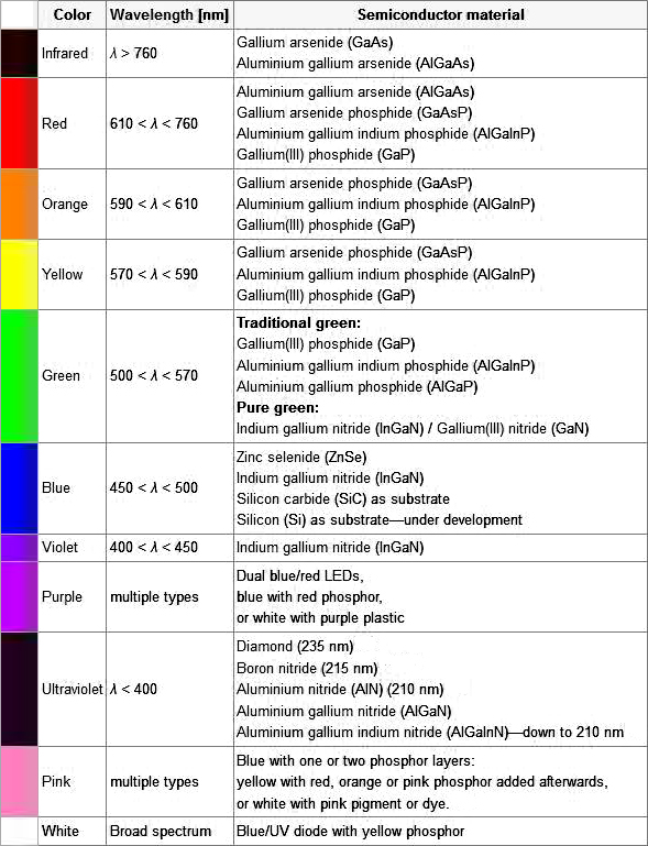
So how does a light emitting diode get its colour. Unlike normal signal diodes which are made for detection or power rectification, and which are made from either Germanium or Silicon semiconductor materials, Light Emitting Diodes are made from exotic semiconductor compounds such as Gallium Arsenide (GaAs), Gallium Phosphide (GaP), Gallium Arsenide Phosphide (GaAsP), Silicon Carbide (SiC) or Gallium Indium Nitride (GaInN) all mixed together at different ratios to produce a distinct wavelength of colour.
Different LED compounds emit light in specific regions of the visible light spectrum and therefore produce different intensity levels. The exact choice of the semiconductor material used will determine the overall wavelength of the photon light emissions and therefore the resulting colour of the light emitted.
Light Emitting Diode Colours
| Typical LED Characteristics | |||
| Semiconductor Material | Wavelength | Colour | VF @ 20mA |
| GaAs | 850-940nm | Infra-Red | 1.2v |
| GaAsP | 630-660nm | Red | 1.8v |
| GaAsP | 605-620nm | Amber | 2.0v |
| GaAsP:N | 585-595nm | Yellow | 2.2v |
| AlGaP | 550-570nm | Green | 3.5v |
| SiC | 430-505nm | Blue | 3.6v |
| GaInN | 450nm | White | 4.0v |
Thus, the actual colour of a light emitting diode is determined by the wavelength of the light emitted, which in turn is determined by the actual semiconductor compound used in forming the PN junction during manufacture.
Therefore the colour of the light emitted by an LED is NOT determined by the colouring of the LED’s plastic body although these are slightly coloured to both enhance the light output and to indicate its colour when its not being illuminated by an electrical supply.
Light emitting diodes are available in a wide range of colours with the most common being RED, AMBER, YELLOW and GREEN and are thus widely used as visual indicators and as moving light displays.
Recently developed blue and white coloured LEDs are also available but these tend to be much more expensive than the normal standard colours due to the production costs of mixing together two or more complementary colours at an exact ratio within the semiconductor compound and also by injecting nitrogen atoms into the crystal structure during the doping process.
From the table above we can see that the main P-type dopant used in the manufacture of Light Emitting Diodes is Gallium (Ga, atomic number 31) and that the main N-type dopant used is Arsenic (As, atomic number 33) giving the resulting compound of Gallium Arsenide (GaAs) crystalline structure.
The problem with using Gallium Arsenide on its own as the semiconductor compound is that it radiates large amounts of low brightness infra-red radiation (850nm-940nm approx.) from its junction when a forward current is flowing through it.
The amount of infra-red light it produces is okay for television remote controls but not very useful if we want to use the LED as an indicating light. But by adding Phosphorus (P, atomic number 15), as a third dopant the overall wavelength of the emitted radiation is reduced to below 680nm giving visible red light to the human eye. Further refinements in the doping process of the PN junction have resulted in a range of colours spanning the spectrum of visible light as we have seen above as well as infra-red and ultra-violet wavelengths.
By mixing together a variety of semiconductor, metal and gas compounds the following list of LEDs can be produced.
Types of Light Emitting Diode
- Gallium Arsenide (GaAs) – infra-red
- Gallium Arsenide Phosphide (GaAsP) – red to infra-red, orange
- Aluminium Gallium Arsenide Phosphide (AlGaAsP) – high-brightness red, orange-red, orange, and yellow
- Gallium Phosphide (GaP) – red, yellow and green
- Aluminium Gallium Phosphide (AlGaP) – green
- Gallium Nitride (GaN) – green, emerald green
- Gallium Indium Nitride (GaInN) – near ultraviolet, bluish-green and blue
- Silicon Carbide (SiC) – blue as a substrate
- Zinc Selenide (ZnSe) – blue
- Aluminium Gallium Nitride (AlGaN) – ultraviolet
Like conventional PN junction diodes, light emitting diodes are current-dependent devices with its forward voltage drop VF, depending on the semiconductor compound (its light colour) and on the forward biased LED current. Most common LED’s require a forward operating voltage of between approximately 1.2 to 3.6 volts with a forward current rating of about 10 to 30 mA, with 12 to 20 mA being the most common range.
Both the forward operating voltage and forward current vary depending on the semiconductor material used but the point where conduction begins and light is produced is about 1.2V for a standard red LED to about 3.6V for a blue LED.
The exact voltage drop will of course depend on the manufacturer because of the different dopant materials and wavelengths used. The voltage drop across the LED at a particular current value, for example 20mA, will also depend on the initial conduction VFpoint. As an LED is effectively a diode, its forward current to voltage characteristics curves can be plotted for each diode colour as shown below.
Light Emitting Diodes I-V Characteristics.

Light Emitting Diode (LED) Schematic symbol and I-V Characteristics Curves
showing the different colours available.
showing the different colours available.
Before a light emitting diode can “emit” any form of light it needs a current to flow through it, as it is a current dependant device with their light output intensity being directly proportional to the forward current flowing through the LED.
As the LED is to be connected in a forward bias condition across a power supply it should be current limited using a series resistor to protect it from excessive current flow. Never connect an LED directly to a battery or power supply as it will be destroyed almost instantly because too much current will pass through and burn it out.
From the table above we can see that each LED has its own forward voltage drop across the PN junction and this parameter which is determined by the semiconductor material used, is the forward voltage drop for a specified amount of forward conduction current, typically for a forward current of 20mA.
In most cases LEDs are operated from a low voltage DC supply, with a series resistor, RSused to limit the forward current to a safe value from say 5mA for a simple LED indicator to 30mA or more where a high brightness light output is needed.
LED Series Resistance.
The series resistor value RS is calculated by simply using Ohm´s Law, by knowing the required forward current IF of the LED, the supply voltage VS across the combination and the expected forward voltage drop of the LED, VF at the required current level, the current limiting resistor is calculated as:
LED Series Resistor Circuit

Light Emitting Diode Example No1
An amber coloured LED with a forward volt drop of 2 volts is to be connected to a 5.0v stabilised DC power supply. Using the circuit above calculate the value of the series resistor required to limit the forward current to less than 10mA. Also calculate the current flowing through the diode if a 100Ω series resistor is used instead of the calculated first.
1). series resistor required at 10mA.

2). with a 100Ω series resistor.

We remember from the Resistors tutorials, that resistors come in standard preferred values. Our first calculation above shows that to limit the current flowing through the LED to 10mA exactly, we would require a 300Ω resistor. In the E12 series of resistors there is no 300Ω resistor so we would need to choose the next highest value, which is 330Ω. A quick re-calculation shows the new forward current value is now 9.1mA, and this is ok.
Connecting LEDs Together in Series
We can connect LED’s together in series to increase the number required or to increase the light level when used in displays. As with series resistors, LED’s connected in series all have the same forward current, IF flowing through them as just one. As all the LEDs connected in series pass the same current it is generally best if they are all of the same colour or type.
LED’s in Series

Although the LED series chain has the same current flowing through it, the series voltage drop across them needs to be considered when calculating the required resistance of the current limiting resistor, RS. If we assume that each LED has a voltage drop across it when illuminated of 1.2 volts, then the voltage drop across all three will be 3 x 1.2v = 3.6 volts.
If we also assume that the three LEDs are to be illuminated from the same 5 volt logic device or supply with a forward current of about 10mA, the same as above. Then the voltage drop across the resistor, RS and its resistance value will be calculated as:

Again, in the E12 (10% tolerance) series of resistors there is no 140Ω resistor so we would need to choose the next highest value, which is 150Ω.
LED Driver Circuits
Now that we know what is an LED, we need some way of controlling it by switching it “ON” and “OFF”. The output stages of both TTL and CMOS logic gates can both source and sink useful amounts of current therefore can be used to drive an LED. Normal integrated circuits (ICs) have an output drive current of up to 50mA in the sink mode configuration, but have an internally limited output current of about 30mA in the source mode configuration.
Either way the LED current must be limited to a safe value using a series resistor as we have already seen. Below are some examples of driving light emitting diodes using inverting ICs but the idea is the same for any type of integrated circuit output whether combinational or sequential.
IC Driver Circuit

If more than one LED requires driving at the same time, such as in large LED arrays, or the load current is to high for the integrated circuit or we may just want to use discrete components instead of ICs, then an alternative way of driving the LEDs using either bipolar NPN or PNP transistors as switches is given below. Again as before, a series resistor, RS is required to limit the LED current.
Transistor Driver Circuit

The brightness of a light emitting diode cannot be controlled by simply varying the current flowing through it. Allowing more current to flow through the LED will make it glow brighter but will also cause it to dissipate more heat. LEDs are designed to produce a set amount of light operating at a specific forward current ranging from about 10 to 20mA.
In situations where power savings are important, less current may be possible. However, reducing the current to below say 5mA may dim its light output too much or even turn the LED “OFF” completely. A much better way to control the brightness of LEDs is to use a control process known as “Pulse Width Modulation” or PWM, in which the LED is repeatedly turned “ON” and “OFF” at varying frequencies depending upon the required light intensity of the LED.
LED Light Intensity using PWM

When higher light outputs are required, a pulse width modulated current with a fairly short duty cycle (“ON-OFF” Ratio) allows the diode current and therefore the output light intensity to be increased significantly during the actual pulses, while still keeping the LEDs “average current level” and power dissipation within safe limits.
This “ON-OFF” flashing condition does not affect what is seen by the human eye as it “fills” in the gaps between the “ON” and “OFF” light pulses, providing the pulse frequency is high enough, making it appear as a continuous light output. So pulses at a frequency of 100Hz or more actually appear brighter to the eye than a continuous light of the same average intensity.
Multi-coloured Light Emitting Diode
LEDs are available in a wide range of shapes, colours and various sizes with different light output intensities available, with the most common (and cheapest to produce) being the standard 5mm Red Gallium Arsenide Phosphide (GaAsP) LED.
LED’s are also available in various “packages” arranged to produce both letters and numbers with the most common being that of the “seven segment display” arrangement.
Nowadays, full colour flat screen LED displays, hand held devices and TV’s are available which use a vast number of multicoloured LED’s all been driven directly by their own dedicated IC.
Most light emitting diodes produce just a single output of coloured light however, multi-coloured LEDs are now available that can produce a range of different colours from within a single device. Most of these are actually two or three LEDs fabricated within a single package.
Bicolour Light Emitting Diodes
A bicolour light emitting diode has two LEDs chips connected together in “inverse parallel” (one forwards, one backwards) combined in one single package. Bicolour LEDs can produce any one of three colours for example, a red colour is emitted when the device is connected with current flowing in one direction and a green colour is emitted when it is biased in the other direction.
This type of bi-directional arrangement is useful for giving polarity indication, for example, the correct connection of batteries or power supplies etc. Also, a bi-directional current produces both colours mixed together as the two LEDs would take it in turn to illuminate if the device was connected (via a suitable resistor) to a low voltage, low frequency AC supply.
A Bicolour LED
 |
| ||||||||||||||||||
Tricoloured Light Emitting Diode
The most popular type of tricolour light emitting diode comprises of a single Red and a Green LED combined in one package with their cathode terminals connected together producing a three terminal device. They are called tricolour LEDs because they can give out a single red or a green colour by turning “ON” only one LED at a time.
These tricoloured LED’s can also generate additional shades of their primary colours (the third colour) such as Orange or Yellow by turning “ON” the two LEDs in different ratios of forward current as shown in the table thereby generating 4 different colours from just two diode junctions.
A Multi or Tricoloured LED
 |
|
LED Displays
As well as individual colour or multi-colour LEDs, several light emitting diodes can be combined together within a single package to produce displays such as bargraphs, strips, arrays and seven segment displays.
A 7-segment LED display provides a very convenient way when decoded properly of displaying information or digital data in the form of numbers, letters or even alpha-numerical characters and as their name suggests, they consist of seven individual LEDs (the segments), within one single display package.
In order to produce the required numbers or characters from 0 to 9 and A to Frespectively, on the display the correct combination of LED segments need to be illuminated. A standard seven segment LED display generally has eight input connections, one for each LED segment and one that acts as a common terminal or connection for all the internal segments.
- The Common Cathode Display (CCD) – In the common cathode display, all the cathode connections of the LEDs are joined together and the individual segments are illuminated by application of a HIGH, logic “1” signal.
- The Common Anode Display (CAD) – In the common anode display, all the anode connections of the LEDs are joined together and the individual segments are illuminated by connecting the terminals to a LOW, logic “0” signal.
A Typical Seven Segment LED Display

Opto-coupler
Finally, another useful application of light emitting diodes is Opto-coupling. An opto-coupler or opto-isolator as it is also called, is a single electronic device that consists of a light emitting diode combined with either a photo-diode, photo-transistor or photo-triac to provide an optical signal path between an input connection and an output connection while maintaining electrical isolation between two circuits.
An opto-isolator consists of a light proof plastic body that has a typical breakdown voltages between the input (photo-diode) and the output (photo-transistor) circuit of up to 5000 volts. This electrical isolation is especially useful where the signal from a low voltage circuit such as a battery powered circuit, computer or microcontroller, is required to operate or control another external circuit operating at a potentially dangerous mains voltage.
Photo-diode and Photo-transistor Opto-couplers

The two components used in an opto-isolator, an optical transmitter such as an infra-red emitting Gallium Arsenide LED and an optical receiver such as a photo-transistor are closely optically coupled and use light to send signals and/or information between its input and output. This allows information to be transferred between circuits without an electrical connection or common ground potential.
Opto-isolators are digital or switching devices, so they transfer either “ON-OFF” control signals or digital data. Analogue signals can be transferred by means of frequency or pulse-width modulation.
XXX . XXX SEMICONDUCTOR LED
the semiconductor emitted by the collision of electrons in Led is a combination of various fuses that are reduced in milli amperes, fuse fuses arranged diagonally in row and column sequences with combinational movements nC ^ r. the fuse's fuse could skip blue; red and white in combinations: LEDs and fuses in electronics are two sides of a coin colliding with einstein's theory E = h V = pv = n RT --- ignoring the postulates E = m C ^ 2 because the molecules in vacuum have the floating mass .

example einstein Parallelum :
With integrated production from LED elements to package and modules, the Panasonic lineup of light emitting diodes (LED) covers various products from standard chip LED to high-brightness white LED. Featuring High heat dissipation, high brightness, and high reliability with our GaN on GaN elements, Panasonic LED offer efficient and cost-effective lighting solutions for various applications, such as LED lighting and display panels.
panasonic offers the best white LEDs for mobile, automotive, lighting, and other applications.
Panasonic's red and infrared laser diode is a dual-wavelength laser that outputs both red and infrared laser lights.

LED Cube
The LED Cube! With a total of 5120 leds, the LED Cube is super bright from every direction! While also being a video player, the LED Cube can be interactive and fun for everyone!
Laser microscope
Do you know why you were told not to drink dirty water? Grab a laser pointer and discover what lurks in Birmingham canal!
M-squared multicolour panel
A demonstration of high quality white light & multi colour panel operating with strips of light emitting diodes. Emitted light in the panel is controlled by the special electronic module, which is controlled through browser-based user interface from a computer.
Colour mixing
Introduction to light: Learn how to bend, bounce and blend light with three high-tech light sources, lenses, mirrors and an activity guide full of fun and learning.
Fibre fuse effect or “Tiny Comet”
The fibre fuse effect is a problem in modern fibre optics telecommunication systems, however, it can make for a stunningly beautiful show!
If a fibre is locally heated to a temperature of 1000C, the laser radiation propagating through the fibre is strongly absorbed by the heated part, increasing its temperature to 104 K. This high-temperature region, seen as a bright white spot, which looks like a comet moving with a velocity of 1 m/s along the fibre.
Laser projection
Create your own laser show using laser diodes, diffractive elements and step motors.on!
Undergraduate projects
This display shows the work of first year electronic engineering students at Aston University. It includes among other things an LED harp, a LED light cube, a mood lamp that demonstrates how different colours can be mixed together to give all colour shades, and a light display that monitors your email inbox.
Diffractive optics
Do you know how light behaves? Really? Get some hands-on experience to see how tiny things make a huge difference!
Interactive LED wall
Did you know most motion sensing technologies use infrared lighting? This demonstration uses infrared sensors to track motion to allow you create beautiful patterns on a LED wall with your hands and body.
Virtual pottery wheel
This virtual pottery wheel allows users to create and adjust a spinning virtual cylinder by passing his or her hand through a laser. When satisfied with the final form, the user can save the customised model.
Diffraction on CD/DVD and smartphone
Ever wonder what the surface of a CD and your smartphone screen looks like? Come and see the wonderful patterns that are generated when a laser strikes these two surfaces.
Light and gummy bears
Have you realised how simple and fun optics can be? Come play with lasers, learn about colours and eat some gummy bears.
Why are optical fibres so useful?
Part 1 – Light Refraction, Optics, TIR
Do you know what glass and the Internet have in common? Find out how fibres that are the width of a single strand of hair make the internet work.
Part 2 – Refractive Index; disappearing objects Behaviour of light travelling through an object is very much dependent on its refractive index. Sounds mysterious? Come and see what this really means and how a clever choice of refractive index can make objects disappear!
Part 3 – TIR, lightguiding Optical fibres have enabled high speed Internet communication. Are you aware how they work? Come and see the science behind modern telecommunication!
Mix your own colours
Have you had a closer look at the screen of your smartphone or a printed newspaper? Are you curious why a picture can be constructed of a mosaic of tiny points of only three colours?
Fun with optics
Take some time out and enjoy a game with a friend. We have a wide selection of fun games to play and to challenge you!
Multicolor LED in integration sphere
Red, green and blue LEDs will be disposed inside a integration sphere. Each LED will be supplied with its own tuneable current source. The integration sphere will mix lots of colours of light to show the full visible spectrum.
Biophotonics for wellbeing and healthy life
Come and see a laser used for non-invasive monitoring of the human physiological parameters at the fingertip. Anyone can try her/himself for blood microcirculation, tissue oxygen saturation, and metabolism efficiency valuation spending just 3-5 min her/his time. In parallel we will demonstrate main principles of optical non-invasive diagnostic devices and their application for human wellbeing and health life support.
Phosphor light converters
Discover wonderful patterns that can be produced with phosphor light converters.
Light and textiles
Collection of art dresses with embedded light elements (luminescent materials, optical fibres, lasers, LEDS etc.) which are inspired by glowing deep sea inhabitants (jellyfish, deep sea fish, sea anemones, squids etc.) will be demonstrated.
Virtual reality with Google cardboard
See how a regular smartphone display can be used to trick your brain into seeing 3D images. We have a range of video demos that are quite simply amazing! (not recommended for people who suffer from epilepsy or prone to motion sickness).
Laser harp
Show us your musical skills on a laser harp. This exciting laser harp is played by blocking individual laser beams which triggers notes on a synthesizer. This project was sponsored by Hobgoblin Music in Birmingham.
Sound modulated onto a laser beam
How is data transmitted over laser beams? Come and see how you can play music from a phone over a laser beam and play this back using a solar panel and speaker.
xxx . xxx LED Chameleon
Create all the colours visible to the human eye through adjusting three LEDs.
Therefore, the interest in optical emission from the integrated Si devices is growing with the main emphasis on infrared emission from forward-biased light-emitting diodes (LED). We will focus here on the visible light emission from the reverse-biased junctions. Silicon (si) is the material of choice in contemporary microelectronics. Due to the large increase of cut-off frequencies of devices, e.g., Si heterojunction bipolar transistor from 100 GHz in 1993, over 200 GHz in 2000 , to over 300 GHz this year , the operating frequency of circuits is increased too. To avoid the negative effects of long electrical transmission lines, optical signal transition for board-to-board, chip-to-chip, and intrachip is proposed .
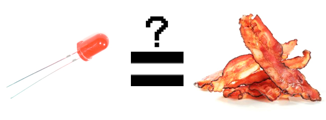
LEDs are all around us: In our phones, our cars and even our homes. Any time something electronic lights up, there’s a good chance that an LED is behind it. They come in a huge variety of sizes, shapes, and colors, but no matter what they look like they have one thing in common: they’re the bacon of electronics. They’re widely purported to make any project better and they’re often added to unlikely things (to everyone’s delight).
Unlike bacon, however, they’re no good once you’ve cooked them. This guide will help you avoid any accidental LED barbecues! First things first, though. What exactly is this LED thing everyone’s talking about?
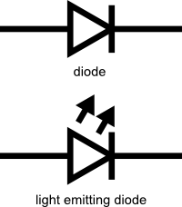
LEDs (that’s “ell-ee-dees”) are a particular type of diode that convert electrical energy into light. In fact, LED stands for “Light Emitting Diode.” (It does what it says on the tin!) And this is reflected in the similarity between the diode and LED schematic symbols:
In short, LEDs are like tiny lightbulbs. However, LEDs require a lot less power to light up by comparison. They’re also more energy efficient, so they don’t tend to get hot like conventional lightbulbs do (unless you’re really pumping power into them). This makes them ideal for mobile devices and other low-power applications. Don’t count them out of the high-power game, though. High-intensity LEDs have found their way into accent lighting, spotlights and even automotive headlights!
Are you getting the craving yet? The craving to put LEDs on everything? Good, stick with us and we’ll show you how!
Suggested Reading
Here are some other topics that will be discussed in this tutorial. If you are unfamiliar with any of them, please have a look at the respective tutorial before you go any further.
How to Use Them
So you’ve come to the sensible conclusion that you need to put LEDs on everything. We thought you’d come around. Let’s go over the rule book:
1) Polarity Matters
In electronics, polarity indicates whether a circuit component is symmetric or not. LEDs, being diodes, will only allow current to flow in one direction. And when there’s no current-flow, there’s no light. Luckily, this also means that you can’t break an LED by plugging it in backwards. Rather, it just won’t work.
The positive side of the LED is called the “anode” and is marked by having a longer “lead,” or leg. The other, negative side of the LED is called the “cathode.” Current flows from the anode to the cathode and never the opposite direction. A reversed LED can keep an entire circuit from operating properly by blocking current flow. So don’t freak out if adding an LED breaks your circuit. Try flipping it around.
2) Moar Current Equals Moar Light
The brightness of an LED is directly dependent on how much current it draws. That means two things. The first being that super bright LEDs drain batteries more quickly, because the extra brightness comes from the extra power being used. The second is that you can control the brightness of an LED by controlling the amount of current through it. But, setting the mood isn’t the only reason to cut back your current.
3) There is Such a Thing as Too Much Power
If you connect an LED directly to a current source it will try to dissipate as much power as it’s allowed to draw, and, like the tragic heroes of olde, it will destroy itself. That’s why it’s important to limit the amount of current flowing across the LED.
For this, we employ resistors. Resistors limit the flow of electrons in the circuit and protect the LED from trying to draw too much current. Don’t worry, it only takes a little basic math to determine the best resistor value to use. You can find out all about it in our resistor tutorial!
Don’t let all of this math scare you, it’s actually pretty hard to mess things up too badly. In the next section, we’ll go over how to make an LED circuit without getting your calculator.
LEDs Without Math
Before we talk about how to read a datasheet, let’s hook up some LEDs. After all, this is an LED tutorial, not a reading tutorial.
It’s also not a math tutorial, so we’ll give you a few rules of thumb for getting LEDs up and running. As you’ve probably put together from the info in the last section, you’ll need a battery, a resistor and an LED. We’re using a battery as our power source, because they’re easy to find and they can’t supply a dangerous amount of current.
The basic template for an LED circuit is pretty simple, just connect your battery, resistor and LED in series. Like this:
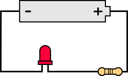
A good resistor value for most LEDs is 330 Ohms. You can use the information from the last section to help you determine the exact value you need, but this is LEDs without math… So, start by popping a 330 Ohm resistor into the above circuit and see what happens.
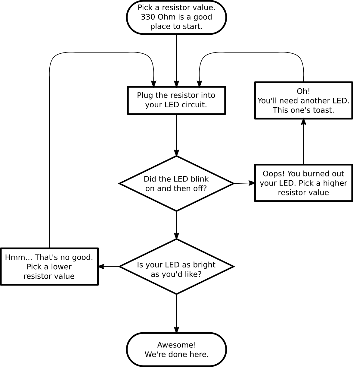
The interesting thing about resistors is that they’ll dissipate extra power as heat, so if you have a resistor that’s getting warm, you probably need to go with a smaller resistance. If your resistor is too small, however, you run the risk of burning out the LED! Given that you have a handful of LEDs and resistors to play with, here’s a flow chart to help you design your LED circuit by trial and error:
Another way to light up an LED is to just connect it to a coin cell battery! Since the coin cell can’t source enough current to damage the LED, you can connect them directly together! Just push a CR2032 coin cell between the leads of the LED. The long leg of the LED should be touching the side of the battery marked with a “+”. Now you can wrap some tape around the whole thing, add a magnet, and stick it to stuff! Yay for throwies!
Of course, if you’re not getting great results with the trial and error approach, you can always get out your calculator and math it up. Don’t worry, it’s not hard to calculate the best resistor value for your circuit. But before you can figure out the optimal resistor value, you’ll need to find the optimal current for your LED. For that we’ll need to report to the datasheet…
Get the Details
Don’t go plugging any strange LEDs into your circuits, that’s just not healthy. Get to know them first. And how better than to read the datasheet.
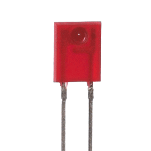
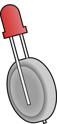
As an example we’ll peruse the datasheet for our Basic Red 5mm LED.
LED Current
Starting at the top and making our way down, the first thing we encounter is this charming table:
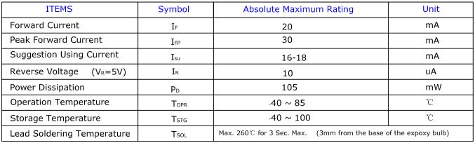
Ah, yes, but what does it all mean?
The first row in the table indicates how much current your LED will be able to handle continuously. In this case, you can give it 20mA or less, and it will shine its brightest at 20mA. The second row tells us what the maximum peak current should be for short bursts. This LED can handle short bumps to 30mA, but you don’t want to sustain that current for too long. This datasheet is even helpful enough to suggest a stable current range (in the third row from the top) of 16-18mA. That’s a good target number to help you make the resistor calculations we talked about.
The following few rows are of less importance for the purposes of this tutorial. The reverse voltage is a diode property that you shouldn’t have to worry about in most cases. The power dissipation is the amount of power in milliWatts that the LED can use before taking damage. This should work itself out as long as you keep the LED within its suggested voltage and current ratings.
LED Voltage
Let’s see what other kinds of tables they’ve put in here… Ah!
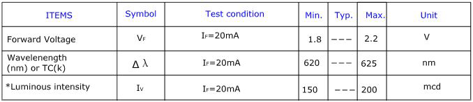
This is a useful little table! The first row tells us what the forward voltage drop across the LED will be. Forward voltage is a term that will come up a lot when working with LEDs. This number will help you decide how much voltage your circuit will need to supply to the LED. If you have more than one LED connected to a single power source, these numbers are really important because the forward voltage of all of the LEDs added together can’t exceed the supply voltage. We’ll talk about this more in-depth later in the delving deeper section of this tutorial.
LED Wavelength
The second row on this table tells us the wavelength of the light. Wavelength is basically a very precise way of explaining what color the light is. There may be some variation in this number so the table gives us a minimum and a maximum. In this case it’s 620 to 625nm, which is just at the lower red end of the spectrum (620 to 750nm). Again, we’ll go over wavelength in more detail in the delving deeper section.
LED Brightness
The last row (labeled “Luminous Intensity”) is a measure of how bright the LED can get. The unit mcd, or millicandela, is a standard unit for measuring the intensity of a light source. This LED has an maximum intensity of 200 mcd, which means it’s just bright enough to get your attention but not quite flashlight bright. At 200 mcd, this LED would make a good indicator.
Viewing Angle
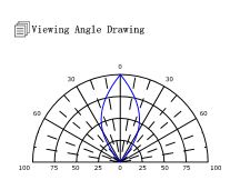
Next, we’ve got this fan-shaped graph that represents the viewing angle of the LED. Different styles of LEDs will incorporate lenses and reflectors to either concentrate most of the light in one place or spread it as widely as possible. Some LEDs are like floodlights that pump out photons in every direction; Others are so directional that you can’t tell they’re on unless you’re looking straight at them. To read the graph, imagine the LED is standing upright underneath it. The “spokes” on the graph represent the viewing angle. The circular lines represent the intensity by percent of maximum intensity. This LED has a pretty tight viewing angle. You can see that looking straight down at the LED is when it’s at its brightest, because at 0 degrees the blue lines intersect with the outermost circle. To get the 50% viewing angle, the angle at which the light is half as intense, follow the 50% circle around the graph until it intersects the blue line, then follow the nearest spoke out to read the angle. For this LED, the 50% viewing angle is about 20 degrees.
Dimensions
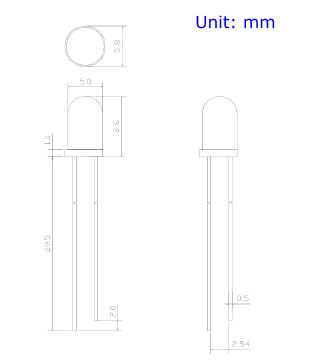
Finally, the mechanical drawing. This picture contains all of the measurements you’ll need to actually mount the LED in an enclosure! Notice that, like most LEDs, this one has a small flange at the bottom. That comes in handy when you want to mount it in a panel. Simply drill a hole the perfect size for the body of the LED, and the flange will keep it from falling through!
Now that you know how to decipher the datasheet, let’s see what kind of fancy LEDs you might encounter in the wild…
Types of LEDs
Congratulations, you know the basics! Maybe you’ve even gotten your hands on a few LEDs and started lighting stuff up, that’s awesome! How would you like to step up your blinky game? Let’s talk about makin' it fancy.
Here’s the cast of characters:

RGB (Red-Green-Blue) LEDs are actually three LEDs in one! But that doesn’t mean it can only make three colors. Because red, green, and blue are the additive primary colors, you can control the intensity of each to create every color of the rainbow. Most RGB LEDs have four pins: one for each color and a common pin. On some, the common pin is the anode, and on others, it’s the cathode.
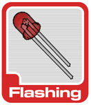
Some LEDs are smarter than others. Take the flashing LED, for example. Inside these LEDs, there’s actually an integrated circuit that allows the LED to blink without any outside controller. Simply power it up and watch it go! These are great for projects where you want a little bit more action but don’t have room for control circuitry. There are even RGB flashing LEDs that cycle through thousands of colors!

SMD LEDs aren’t so much a specific kind of LED but a package type. As electronics get smaller and smaller, manufacturers have figured out how to cram more components in a smaller space. SMD (Surface Mount Device) parts are tiny versions of their standard counterparts. SMD LEDs come in several sizes, from fairly large to smaller than a grain of rice! Because they’re so small, and have pads instead of legs, they’re not as easy to work with, but if you’re tight on space they might be just what the doctor ordered.

High-Power LEDs, from manufacturers like Luxeon and CREE, are crazy bright. Generally, an LED is considered High-Power if it can dissipate 1 Watt or more of power. These are the fancy LEDs that you find in really nice flashlights. Arrays of them can even be built for spotlights and automobile headlights. Because there’s so much power being pumped through the LED, these often require heatsinks. A heatsink is basically a chunk of heat conducting metal with lots of surface area whose job is to transfer as much waste heat into the surrounding air as possible. High-Power LEDs can generate so much waste heat that they’ll damage themselves without proper cooling. Don’t let the term “waste heat” fool you, though, these devices are still incredibly efficient compared to conventional bulbs.
There are even LEDs that emit light outside of the normal visible spectrum. You probably use Infrared LEDs every day, for instance. They’re used in things like TV remotes to send small pieces of information in the form of invisible light! On the opposite end of the spectrum you can also get Ultraviolet LEDs. Ultraviolet LEDs will make certain materials fluoresce, just like a blacklight! They’re also used for disinfecting surfaces, because many bacteria are sensitive to UV radiation.
With fancy LEDs like these at your disposal, there’s no excuse for leaving anything un-illuminated. However, if your thirst for LED knowledge hasn’t been slaked, then read on, and we’ll get into the nitty-gritty on LEDs, color, and luminous intensity!
Delving Deeper
So you’ve graduated from LEDs 101 and you want more? Oh, don’t worry, we’ve got more. Let’s start with the science behind what makes LEDs tick… err… blink. We’ve already mentioned that LEDs are a special kind of diode, but let’s delve a little deeper into exactly what that means:
What we call an LED is really the LED and the packaging together, but the LED itself is actually tiny! It’s a chip of semiconductor material that’s doped with impurities which creates a boundary for charge carriers. When current flows into the semi-conductor, it jumps from one side of this boundary to the other, releasing energy in the process. In most diodes that energy leaves as heat, but in LEDs that energy is dissipated as light!
The wavelength of light, and therefore the color, depends on the type of semiconductor material used to make the diode. That’s because the energy band structure of semiconductors differs between materials, so photons are emitted with differing frequencies. Here’s a table of common LED semiconductors by frequency:
Truncated table of semiconductor materials by color. The full table is available on the Wikipedia entry for “LED”
While the wavelength of the light depends on the band gap of the semiconductor, the intensity depends on the amount of power being pushed through the diode. We talked about luminous intensity a little bit in a previous section, but there’s more to it than just putting a number on how bright something looks.
The unit for measuring luminous intensity is called the candela, although when you’re talking about the intensity of a single LED you’re usually in the millicandela range. The interesting thing about this unit is that it isn’t really a measure of the amount of light energy, but an actual measure of “brightness”. This is achieved by taking the power emitted in a particular direction and weighting that number by the luminosity function of the light. The human eye is more sensitive to some wavelengths of light than others, and the luminosity function is a standardized model that accounts for that sensitivity.
The luminous intesity of LEDs can range from the tens to the tens-of-thousands of millicandela. The power light on your TV is probably about 100 mcd, whereas a good flashlight might be 20,000 mcd. Looking straight into anything brighter than a few thousand millicandela can be painful; don’t try it.
Forward Voltage Drop
Oh, I also promised that we’d talk about the concept of Forward Voltage Drop. Remember when we were looking at the datasheet and I mentioned that the Forward Voltage of all of your LEDs added together can’t exceed your system voltage? This is because every component in your circuit has to share the voltage, and the amount of voltage that every part uses together will always equal the amount that’s available. This is called Kirchhoff’s Voltage Law. So if you have a 5V power supply and each of your LEDs have a forward voltage drop of 2.4V then you can’t power more than two at a time.
Kirchhoff’s Laws also come in handy when you want to approximate the voltage across a given part based on the Forward Voltage of other parts. For instance, in the example I just gave there’s a 5V supply and 2 LEDs with a 2.4V Forward Voltage Drop each. Of course we would want to include a current limiting resistor, right? How would you find out the voltage across that resistor? It’s easy:
5 (System Voltage) = 2.4 (LED 1) + 2.4 (LED 2) + Resistor5 = 4.8 + ResistorResistor = 5 - 4.8Resistor = 0.2
So there is .2V across the resistor! This is a simplified example and it isn’t always this easy, but hopefully this gives you an idea of why Forward Voltage Drop is important. Using the voltage number you derive from Kirchhoff’s Laws you can also do things like determine the current across a component using Ohm’s Law. In short, you want your system voltage equal to the expected forward voltage of your combined circuit components.
Resources and Going Further
You’ve made it! You know, like, almost everything… about LEDs. Now go forth and put LEDs on whatever you please!
If you’d like to learn more about some LED related topics, visit these other tutorials:
- Light
- IR Communication
- RGB Panel Hookup Guide
- Das Blinken Top Hat
- LED Display Driver Hookup Guide
- Interactive Hanging LED Array - Create a giant LED array driven by the Arduino Pro Mini.
- T³: Using LEDs as Light Sensors - Using an LED as a light detector!
xxx . xxx Get what you need for LED driver protection
Selecting the right fuses will help engineers optimize lighting durability, lifespan, cost, and form factor.
Selecting the right type of circuit protection for a light-emitting-diode (LED) driver can be challenging because system demands vary greatly, depending on the application and power source. However, introducing a few key parameters will help designers dial in on the right component for the job.
Designing new generations of drivers requires knowledge of a wide range of power supply topologies and circuit protection choices. Selecting the right fuses will help engineers optimize lighting durability, lifespan, cost, and form factor.
A single LED typically requires a voltage of 2 to 4 Vdc and constant current to ensure optimal performance and long life. For this reason, all LED lighting solutions need a driver circuit that provides steady voltage and current levels for each LED or LED string. The complexity of the LED driver can range from a very simple 1-W dc/dc converter to a more than 100-W dc/dc or ac/dc converter with power factor correction (PFC).
Older designs rely on simple resistors to limit LED-drive current. A small change in forward voltage results in large forward current in the junction. This will overheat the LED junction. As the junction temperature increases, the forward voltage decreases, producing large current in the junction. This chain of events leads to thermal runaway and LED failure. To eliminate this type of failure, proper current protection in the LED driver circuit is required.
.jpg)
Fig. 1: Block diagram of a complex LED driver.
LEDs are driven by constant current. If the LED junction temperature increases, the forward voltage of the driver decreases, causing the driver to overheat. In this case, the driver itself must be protected against overcurrent and overvoltage to prevent thermal runaway. Without protection, there is a high risk of damaging both the driver and the LED itself. This is a critical reason that circuit protection is mandatory in most markets around the world.
To determine what type of circuit protection is required for a specific LED application, it is important to know where it is needed and the typical operating parameters for the application. Additionally, knowing the difference between primary and secondary overcurrent protection will help designers choose the appropriate fuse selection. Specific application metrics for voltage rating, current rating, temperature de-rating, and interrupting rating also help to determine the component choice.
LED drivers powered by the electrical grid must have overcurrent and short circuit protection. This is driven by UL, IEC, and other safety agency requirements. Typically, time-delay and one-time fuses are used for the driver protection because they can tolerate the high inrush currents when power is initially switched on. Additionally, the fuses can be very small, making them easily integrated into consumer LED light bulbs.
Consider the following parameters for LED driver fuse selection:
1. Voltage rating — For 110- to 230-V grid-powered LED applications, a 250-Vac-rated fuse is needed. Note that select countries demanding 277- or 347-V capable solutions require a higher-rated fuse.
2. Current rating — This is determined by the power output of the driver. Select a fuse rating that is 20% higher than the nominal LED driver current (select 1-A-rated fuse for a driver with 800 mA nominal current).
3. Interrupting rating — This determines the maximum current that the fuse can safely interrupt during short circuits.
4. Temperature derating — Fuses at higher temperatures open at lower currents. The fuse current rating (See Fig. 2) must be derated according to the ambient temperature level. During operation, LEDs generate high levels of heat, which must be conducted away from the printed circuit board. Derating is critical for fuses used close to the light source.

Fig.2: Fuse temperature rating.
5. Melting integral (I2t) — LED drivers tend to draw larger currents at power-up due to the initial charging from input capacitors, so a fuse with larger melting integral (I2t) capability makes an ideal choice.
6. Required agency approvals — Depending on the country of the final lighting device installation, applications may require certification from UL or IEC.
7. Mechanical considerations (size, shape, etc) — LED drivers typically require fuses as small as possible. Chip fuses starting at 0603-size are available for lower-voltage drivers, and for grid-powered drivers, subminiature radial leaded is the popular choice.
Battery-powered LED solutions or subsystems can be protected separately. If only one LED light source is malfunctioning, protecting subsystems is a good way to avoid complete system shutdown.
New applications for LED lighting and illumination technologies are popping up in several industries, including:
• Internet of Things (IoT) — Integrated lighting, heating and security systems, hubs and servers, and smart phones, digital TVs, and appliances.
• Medical instruments, monitors, lighting and emergency systems for hospitals, doctors’ offices, and home health care.
• Automotive and aeronautics — Interior and exterior lighting, headlights, instrumentation and emergency systems for automobiles, as well as roadway and signal lighting.
• Telecommunications — Lighting, energy and emergency controls for server farms, indicators for switches, routers and hubs, lighting and monitoring for enterprise computer systems.
• Industrial — Illumination for handsets, remote equipment, environmental monitors, security systems and industrial sensors, and specialty LED lighting for applications such as food processing plants to refineries.
Eaton has a large selection of circuit protection products to satisfy just about every LED driver circuit requirement. Selecting the ideal fuse to protect against overcurrent and overvoltage is essential to ensuring the long life and reliability of LEDs. The appropriate circuit protection can also help designers optimize driver size and cost for all markets around the world.

XXX . XXX Education in Microscopy and Digital Imaging
Among the most promising of emerging technologies for illumination in optical microscopy is the light-emitting diode (LED). These versatile semiconductor devices possess all of the desirable features that incandescent (tungsten halogen) and arc lamps lack, and are now efficient enough to be powered by low-voltage batteries or relatively inexpensive switchable power supplies. The diverse spectral output afforded by LEDs makes it possible to select an individual diode light source to supply the optimum excitation wavelength band for fluorophores spanning the ultraviolet, visible, and near-infrared regions. Furthermore, newer high-power LEDs generate sufficient intensity to provide a useful illumination source for a wide spectrum of applications in fluorescence microscopy (see Table 1), including the examination of fixed cells and tissues, as well as live-cell imaging coupled to Förster resonance energy transfer (FRET) and lifetime measurement (FLIM) techniques. The full width at half maximum (FWHM; bandwidth) of a typical quasi-monochromatic LED varies between 20 and 70 nanometers (see Figure 1), which is similar in size to the excitation bandwidth of many synthetic fluorophores and fluorescent proteins. As compiled in Table 1, LEDs having output wavelengths in the 400-465 nanometer range exhibit power levels exceeding 20 milliwatts/cm2, whereas most of the longer wavelength-emitting LEDs (green through red) have power outputs of less than 10 milliwatts/cm2. The broad spectral profile of several LEDs in the 535 to 585 nanometer region is due to the fact that these diodes incorporate a secondary phosphor that is excited by a violet or ultraviolet primary LED, thus reducing power output and broadening the spectral profile. Thus, the green to yellow-orange excitation region, one of the most useful for common fluorophores such as TRITC, MitoTrackers, and orange or red fluorescent proteins, remains a downside for those applications (such as FRAP and photoactivation) that require high light levels.

Compared to laser light, the wider bandwidth featured by LEDs is more useful for exciting a variety of fluorescent probes, and compared to the excessive heat and continuous spectrum emitted by arc lamps, LEDs are cooler, smaller, and provide a far more convenient mechanism to cycle the source on and off, as well as to rapidly select specific wavelengths. Commercial LED illumination units designed for fluorescence microscopy have been introduced by several manufacturers, and despite their weaker emission intensity when compared to the bright spectral lines of mercury and metal halide arc lamps, current trends in LED development point to the expectation of significant increases in brightness throughout all wavelength regions in the next few years. Furthermore, recent advances in LED technology targeted at producing die crystals having a geometry that decreases light loss through internal reflection should help generate devices that can be incorporated into virtually all applications in fluorescence microscopy. Illustrated in Figure 1 are the LED emission spectral profiles for several commercially available diodes. The spectra were recorded at the microscope objective focal plane using a broadband mirror positioned in a fluorescence optical block. Power levels for these LEDs are listed in Table 1 using both a mirror and common fluorescence filter sets.
In contrast to arc lamps, which exhibit a high degree of intrinsic radiance or brightness, LED technology has slowly evolved from rudimentary devices that were capable of providing only a thousandth of a lumen of red light in the late 1960s. During the past four decades, however, LEDs have advanced at a pace that rivals microprocessors. Similar to the prediction by Gordon E. Moore that the number of transistors on a computer chip would double every two years, Agilent Technologies scientist Roland Haitz predicted that the brightness of LEDs would increase by a factor of 20 every 10 years. In fact, what is now termed Haitz' Law has proven to be reliable because LEDs have historically doubled in brightness every two years and are expected to continue this dramatic growth in performance. As their brightness and the range of available colors has increased, LEDs have been put to use in a variety of new applications, including the role of an energy-efficient and durable replacement for incandescent lamps for home and industrial lighting. In addition, high-performance LEDs are now being used in a variety of other industrial, medical, and military applications. Among the many examples are navigation, robotics, machine vision, endoscopy, and diagnostic instrumentation. In the future, there should be an increasing demand for high brightness light sources based on LED devices in areas of the economy that have substantially more market power than optical microscopy. This demand will no doubt provide a driving force for the development of powerful LEDs emitting in all spectral regions, thus benefiting all illumination modalities in optical microscopy.
Many of the initial attempts to employ LEDs as light sources for microscopy failed in part because of the low radiant output of early devices. In general, the previously patented designs for microscope illumination were based on large numbers of LEDs grouped to generate a uniform pattern of illumination. This approach produced a relatively high radiant flux level, but failed to address the low radiance that results from such a large, distributed light source (in contrast to the point source characteristics of an arc-discharge lamp). Currently available high-performance LEDs are sufficiently bright to function individually as a highly effective source of monochromatic light having low spatial coherence for observations in fluorescence epi-illumination or with polychromatic light in transmitted microscopy. Although their averaged spectral irradiance is still lower than that of the spectral peaks from the powerful HBO (mercury) 100-watt arc-discharge lamp, it is approaching that of the XBO (xenon) 75-watt arc lamp continuum in many of the visible portions of the spectrum.
LEDs are considerably more efficient than arc-discharge lamps at converting electricity into visible light, often achieving outputs of up to 100 lumens per watt compared to the 22 lumens per watt for an HBO 100-watt source. These semiconductor devices are rugged and compact, and can often survive for 100,000 hours in use, or approximately 500 times longer than an HBO mercury lamp. Several of the green LEDs have conversion efficiencies as high as 75 percent, although devices in this wavelength range still suffer from reduced power output. In contrast, violet and blue LEDs having light outputs of 250 and 150 milliwatts, respectively, are now commercially available and similar powers in other wavelengths should be available in the near future. The output of LEDs can be modulated at high frequencies (up to 5 kilohertz) and their output brightness can be regulated by controlling the available current. These advantageous features eliminate the requirement for mechanical shutters as well as neutral density filters to control illumination of the specimen in microscopy applications. Although LEDs feature relatively narrow spectral emission profiles, in most cases they must still be used with interference thin-film excitation filters to remove the residual wavelengths on the extremes (at the spectral tails).
Optical Power of LEDs
| ||||||||||||||||||||||||||||||||||||||||||||||||||||||||||||||||||||||||||||||||||||||||||||||||||
Table 1
Presented in Table 1 are the optical output power values and FWHM spectral bandwidths for several near-ultraviolet and visible emitting LEDs that are currently used in fluorescence microscopy. The power for each LED is catalogued in milliwatts/cm2 and was measured at the output of a liquid light guide (LLG column in Table 1) as well as the focal plane of the microscope objective (40x fluorite dry, numerical aperture = 0.85) using a photodiode-based radiometer. Either a mirror with greater than 95% reflectivity from 350 to 800 nanometers or a standard fluorescence filter set was used to project light through the objective and into the radiometer sensor (values listed in columns labeled Mirror and Filter Set, respectively, in Table 1). The light throughput loss in a microscope illumination system can vary between 95 and 99 percent of the input power, depending upon the number of filters, mirrors, prisms, and lenses in the optical train. For a typical research-grade inverted microscope coupled to an external LED illumination source, less than 3 percent of the light exiting the liquid light guide is available for excitation of fluorophores positioned at the objective focal plane. A similar degree of light loss occurs with external metal halide light sources coupled to the microscope through a liquid light guide, as well as traditional xenon and mercury arc discharge lamps secured directly to the illuminator through a lamphouse.
In commercial LED lamphouses, individual diode modules can be readily interchanged to achieve excitation bandwidths suitable for the various fluorophores used in each experiment. The intensity of each LED module can also be independently adjusted in precise electrical steps (percentages of maximum output) so that illumination excitation periods can be balanced with detector sensitivity to avoid specimen phototoxicity. Another advantage of LEDs is their ability to instantly illuminate at full intensity once the electrical current is applied. Unlike arc-discharge and incandescent lamps, LEDs can be repeatedly modulated, or switched on and off, without suffering deleterious effects on their life span. Furthermore, without mechanical parts, the all-electronic diode illumination system is free of the problematic vibrations produced by shutter and neutral density filter motion.

A unique aspect of LED illumination is the outstanding spatial and temporal stability (compared to traditional illumination sources), which enables highly accurate quantitative analysis techniques for extended periods. LEDs are governed by the fully reversible photoelectric effect during operation. As a result, LEDs feature the lowest operating temperatures of all light sources in optical microscopy and are among the most stable in temporal and spatial terms, as well as wavelength distribution. Furthermore, provided LEDs are operated at the proper voltage and current, they feature a significantly longer lifetime than any of the other currently available light sources (see Figure 2). Mercury and xenon arc lamps have a lifespan of 200 to 400 hours (respectively), whereas metal halide sources last 2,000 hours or more. Tungsten-halogen incandescent lamps have lifetimes ranging from 500 to 2,000 hours, depending on the operating voltage. In contrast, many LED sources exhibit lifetimes exceeding 10,000 hours without a significant loss of intensity, and some manufacturers guarantee a lifetime of 100,000 hours before the source intensity drops to 70 percent of the initial value.
All lamps that produce a significant level of heat, including LEDs, also exhibit a dependence of emission output on the source temperature. For incandescent and arc lamps, a period of up to one hour is required until the illumination source is sufficiently stable to enable reproducible measurements or to gather time-lapse video sequences without significant temporal variations in intensity. This long waiting period is not necessary for LEDs, which are capable of reacting extremely fast (within a few microseconds). However, the highest power versions can also generate a significant amount of heat (approaching 60 to 70 percent of their output) during warm-up and, due to their high speed, are affected by high-frequency instability in the power supply. When operating LEDs, a change in current can produce a shift of the emission peak that is similar in magnitude to that seen in the lines of arc lamps. This effect often occurs if the LED die is not perfectly homogeneous, and the size of the shift often depends on the type and quality of the semiconductor crystal used in fabricating the device. Wavelength stability can be ensured when using LEDs by calibrating the spectral output with operating current prior to initiating experiments.
Silicon diodes emit light in the near-infrared (IR) region, but diodes made from other semiconductors can emit in the visible and near-ultraviolet (UV) wavelengths. A typical LED source consists of a semiconductor crystal ranging from approximately 0.3 x 0.3 millimeters to 1 or 2 square millimeters in size. The most common crystals used in the fabrication of LEDs are based on mixtures of periodic table Group III and Group V elements, such as GaN (gallium nitride), SiC (silicon carbide), ZnSe (zinc selenide), and GaAlAsP (a mixture of gallium, aluminum, arsenic, and phosphorous). Each of these crystals emits in a different waveband (see Figure 1 and Table 2). Careful control of the relative semiconductor proportions, as well as the addition of dopants to alter the electronic properties of the crystalline lattice, enables manufacturers and researchers to produce diodes that emit red, orange, yellow, or green light. The spectral bandwidth of these emissions typically ranges between 12 and 40 nanometers with no significant out-of-band components in the infrared or ultraviolet wavelengths (spectral regions detrimental to live cell imaging). The application of silicon carbide and gallium nitride in LEDs has resulted in devices that emit in the blue region (useful for excitation of cyan, green, and yellow fluorescent protein variants), while combining several colors in different proportions can generate various color temperatures of white light for transmitted microscopy applications.

In a typical configuration for optical microscopy illumination, one or more dies are embedded into a larger LED structure for protection and more efficient light collection, as well as the ease of electrical connection and thermal handling. Among the primary advantages of LED technology is that small individual units can be combined to engineer a light source having the shape best suited to a particular application. Possible source geometries are limited only by heat dissipation and the permitted package density of the surface mount device (SMD) technology used to integrate a number of dies onto the printed circuit board. In this manner, very dense, bright, custom-designed light sources can be fabricated to match the input collection parameters of the target optical system. In microscopy, multiple LEDs can be packed into a compact and efficient internal or external light source that emits a high flux of quasi-monochromatic photons from a small area to completely fill the objective (or condenser) aperture.
Basic Properties of LEDs
The fundamental characteristics of LEDs are distinct from those of other illumination sources commonly employed for optical microscopy. As such, LEDs comprise a unique category of non-coherent light sources that are capable of producing continuous and efficient illumination from a simple twin-element semiconductor diode (termed a chip or die) encased in a clear epoxy housing that, in many cases, also serves double duty as a projection lens. The overall concept surrounding LED operation is extremely simple. One of the two semiconductor regions in the chip is dominated by negative charges (the n region), while the other is dominated by positive charges (the p region). When sufficient voltage is applied to the electrical leads, a current is created as electrons transition across the junction between the two semiconductors from the n region into the p region where the negatively charged electrons combine with positive charges. The intermediate area or junction between the two semiconductors is known as the depletion region (see Figure 3). Each recombination of charges that occurs in the depletion region is associated with a reduction in energy level (equal to the charge times the band gap, V(g), of the semiconductor), which may release a quantum of electromagnetic radiation in the form of a photon having an energy (and wavelength) equal to the band gap energy. The wavelength bandwidth of emitted photons is a characteristic of the semiconductor material (see Table 2), therefore, different colors can readily be achieved by making changes to the semiconductor composition of the chip.
Light-Emitting Diode Color Variations
| |||||||||||||||||||||||||||||||||||||||||||||||
Table 2
As semiconductor materials, LEDs have properties common to elements in the silicon category of the periodic table and display variable electrical conduction characteristics. Typical semiconductors exhibit electrical resistances values that are intermediate between those of conductors and insulators, and their behavior is modeled in terms of the electronic band theory for solids. In a crystalline solid, electrons occupy a large number of energy levels that are grouped together into nearly continuous energy bands, the width and spacing of which differ considerably with the specific properties of the material. At higher energy levels two distinct bands, termed the valence and conduction bands, are used to define the band gap for a particular material. Valence band electrons, which form fixed localized bonds between atoms in a solid, have lower energy than the highly mobile conduction band electrons. Conductors have overlapping valence and conduction bands that enable the transition of valence electrons into the conduction band to produce holes (vacancies with a net positive charge) in the valence band. Electrons from adjacent atoms can easily migrate through the lattice into holes, thus creating a movement of vacancies in the opposite direction. In contrast, insulators have fully occupied valence bands and much larger band gaps that require significant energy input in order to displace valence electrons into the conduction band.
The band gaps in semiconductors are small, but finite, and at room temperature, mere thermal agitation is sufficient to move some electrons into the conduction band. Most of the electronic devices incorporating semiconductors (such as diodes and transistors) are designed so that application of a voltage is required to produce the changes in electron distribution between the valence and conduction bands necessary to permit current flow. There are large differences in the band gap potential between different semiconductors, although the band arrangement is similar in all of these materials. Silicon, which is the simplest intrinsic semiconductor, does not have the appropriate band gap structure to be useful by itself in LED construction (but silicon is still used in many other devices, including integrated circuits). However, the conduction characteristics of silicon can be improved by doping (Figure 3), which introduces minute quantities of impurities to generate additional electrons or vacancies (holes) in the native crystalline structure.
The process of doping is best described using the element silicon, a Group IV member of the periodic table. Silicon has four valence electrons that participate in bonding with neighboring atoms in the pure crystal, leaving no deficit or excess. If a small amount of a Group III element (having three valence electrons) is mixed into solid silicon, an insufficient number of electrons are now available to satisfy all bonding requirements, creating holes in the crystal and producing a net positive charge to classify the doped silicon as a p-type semiconductor. Boron is one of the elements that is commonly utilized to dope pure silicon to achieve p-type characteristics. In contrast, adding a Group V element, such as phosphorus (having five valence electrons), to pure silicon generates an n-type semiconductor that has a net negative charge due to the extra valence electrons. The two most common semiconductor elements, silicon and germanium, are generally unsuitable for construction of LEDs due to the significant amount of heat produced at the junctions as well as their low emission levels of visible and infrared light.
Photon-emitting diode p-n junctions are typically based on a mixture of Group III and Group V elements, such as gallium, arsenic, phosphorous, indium, and aluminum. The relatively recent addition of silicon carbide and gallium nitride to this semiconductor palette has yielded blue-emitting diodes, which can be combined with other colors or secondary phosphors to produce LEDs that emit white light. The fundamental key to manipulating the properties of LEDs is the electronic nature of the p-n junction between two different semiconductor materials. When dissimilar doped semiconductors are fused, the flow of current into the junction and the wavelength characteristics of the emitted light is determined by the electronic character of each material. In general, current will readily flow in one direction across the junction, but not in the other, constituting the basic diode configuration. This type of behavior is best understood in terms of the transition of electrons and holes in the two materials and across the junction. Electrons from the n-type semiconductor move to the positively doped (p-type) semiconductor, which has vacant holes, allowing electrons to "jump" from hole to hole. The result of this migration is that holes appear to move in the opposite direction, or away from the positively charged semiconductor toward the negatively charged semiconductor. Electrons from the n-type region and holes from the p-type region recombine in the vicinity of the junction to form the depletion region (Figure 3), in which no charge carriers remain. Thus, a static charge is established in the depletion region that inhibits current flow unless an external voltage is applied.

In order to configure a diode, electrodes are placed on the opposite ends of a p-n semiconductor device to apply a voltage that is capable of overcoming the effects of the depletion region. Typically, the n-type region is connected to the negative terminal and the p-type region is connected to the positive terminal (known as forward biasing the junction) so that electrons will flow from the n-type material toward the p-type and holes will move in the opposite direction. The net effect is that the depletion zone disappears and electrical charge moves across the diode with electrons driven to the junction from the n-type material, whereas holes are driven to the junction from the p-type material. The combination of holes and electrons flowing into the junction enables a continuous current to be maintained across the diode. Although control of the interaction between electrons and holes at the p-n junction is a fundamental element in the design of all semiconductor diodes, the primary goal of LEDs is the efficient generation of light. The production of visible light due to injection of charge carriers across the p-n junction only takes place in semiconductor diodes having specific material compositions, which has led to the search for new combinations that feature the necessary band gap between the conduction band and orbitals of the valence band. Furthermore, research is ongoing to design LED architectures that minimize absorption of light by the diode materials and are more robust at concentrating light emission in a specific direction.
LED Construction
Among the critical aspects of LED fabrication are the nature of the elements used for the n-type and p-type semiconductors, as well as their physical geometry, design of the device housing, and configuration of the light escape route. The basic structure of a typical LED consists of the semiconductor material (the die or chip), a frame on which the die is mounted, and the encapsulation material surrounding the assembly (see Figure 4). In most cases, the LED semiconductor is supported in a reflector cup that is attached to an electrode (the cathode), while the top face of the chip is connected with a gold bonding wire to a second electrode (the anode). Several of the more complex junction structure designs require two bonding wires, one for each electrode. In addition to the obvious variation in the radiation wavelength of different LEDs, there are also variations in shape, size, and radiation pattern. Semiconductor LED chips range in size up to several square millimeters, and the housing/lens system varies between 2 and 10 millimeters in diameter. Most commonly, the BODY of the LED features a hemispherical geometry, but they may also be rectangular, square, triangular, or polygonal.
Presented in Figure 4 are the architectural details of two popular LED package designs. The conventional lead-frame hemispherical 5-millimeter LED featured in Figure 4(a) is commonly used as an indicator lamp for electronic appliances. Epoxy resins are used to cast the encapsulant system in these LEDs, which also feature cylindrical and rectangular lens geometries. The die is secured in a conical reflector cup that is soldered to the cathode lead and the anode is connected to the die with a bonding wire. Light emerging from the sides of the LED is reflected by the cup into the epoxy BODY. A flat cast into the base of the epoxy dome serves as an indicator of lead polarity. Typically, these indicator LEDs contain a die that measures 0.25 to 0.3 millimeters on the side, while the lens diameter ranges from 2 to 10 millimeters. The high-power GaInN flip chip diode cross section illustrated in Figure 4(b) is build on an aluminum or copper heat sink slug that can be soldered onto a printed circuit board for more efficient heat removal. Encapsulating the die is a protective silicone layer designed to overcome total internal reflection of emitted wavefronts and direct them through the larger plastic lens. A gold wire serves to connect the large cathode lead to the die, which is mounted on a silicon chip for protection against electrostatic discharge. The anode (not shown) is similar in configuration to the cathode, but projects away from the package in the opposite direction. LEDs of this design are currently the preferred choice for illumination in fluorescence microscopy.
The emission color of an LED is determined by the combination of semiconductors used in the fabrication process, whereas the optical characteristics are generally controlled by variables in the packaging. The beam angle can range from narrow to wide (see Figure 5), and is determined by the shape of the reflector cup, the size and design criteria of the semiconductor, the distance from the chip surface to the top of the housing or lens system, and the geometry of the lens. LED emission profiles can generally be divided into two classes: edge emitters (Figure 4(a)) and surface emitters (Figure 4(b)). Most surface emitters exhibit a Lambertian emission pattern (see Figure 5(d)) where the intensity profile is proportional to the cosine of the emission angle, which is measured from the axis perpendicular to the die surface. In contrast, edge emitters typically emit light from a small region (approximately 50 micrometers in size) on the sides of the die in a complex pattern that is axis-dependent. The light escaping from an edge emitter is non-symmetrical, with a fast axis perpendicular to the lateral edge dimension, and a slow axis parallel to the die. In order to focus and collimate the light from all four sides of an edge-emitter LED, the die is usually housed inside a reflective cup (Figure 4(a)) at the expense of expanding the source size.
Illustrated in Figure 5(d) are far-field emission patterns for LEDs featuring planar (Figure 5(a)), hemispherical (Figure 5(b)), and parabolic (Figure 5(c)) lenses. The three emission patterns in Figure 5(d) are normalized and overlaid for comparison purposes. Note that at F=60°, the planar Lambertian diode emission pattern decreases to 50 percent of its maximum value, whereas the hemispherical LED features a more symmetrical distribution. Tinting that is applied to some epoxy lenses does not determine the emission color of an LED, but rather is used as a convenient indicator of the lamp color when inactive. LED designs targeted for applications that require high intensity (such as fluorescence microscopy) usually feature clear lenses without tint or diffusion additives. This configuration produces the greatest level of light output and is usually designed to feature a custom-shaped beam for the most efficient transfer of light into a collection or projection lens system. Alternatively, diffusion-type LED lenses contain embedded glass particles that spread the emitted light cone into a larger angle. This lens style is commonly employed in applications in which the LED is viewed directly, such as for indicator lamps on equipment panels.

The choice of materials and fabrication techniques for LED construction is guided by two primary targets: the maximization of light generation in the hybrid semiconductor materials and the efficient extraction of the light created by the device. In typical p-n junctions, electrons and holes from n-type and p-type materials (the majority carriers) are injected across the junction to establish the flow of current and to produce light (radiative recombination) in a specific wavelength band. This process is often hampered by non-radiative recombination of minority carriers (electrons in p-type materials and holes in n-type materials) with majority carriers. In addition, the presence of impurities, structural dislocations, and other crystalline defects in semiconductor materials can lead to non-radiative recombination events, which do not result in emission of a photon. Thus, one of the primary goals in LED design is to maximize the radiative recombination of charge carriers by careful selection of suitable semiconductor materials to provide the appropriate band structure in order to produce favorable quantum efficiency values. Another important goal, as discussed in greater detail below, is to ensure that the greatest possible amount of light generated by an LED is able to escape the device and be used for illumination.
The wavelength (and color) of light emitted by a semiconductor diode is determined by the difference in energy between the recombining electron-hole pairs of the valence and conduction bands, as previously described. The approximate energies of the carriers correspond to the upper energy level of the valence band and the lowest energy of the conduction band. As a result, the wavelength (l) of an emitted photon is approximated by the following expression:
l = hc/Ebg
where h represents Planck's constant, c is the velocity of light, and Ebg is the band gap energy. In order to modulate the wavelength of emitted radiation, the band bap of the semiconductor material utilized to fabricate the diode must be carefully selected. Gallium arsenide is a popular diode material and serves as an excellent example of how a semiconductor band structure can be altered to vary the LED emission wavelength. The band gap of gallium arsenide is approximately 1.4 electron-volts, which produces emission at approximately 900 nanometers, in the near-infrared region. In order to increase the frequency of emission to achieve wavelengths in the visible red region (650 nanometers), the band gap must be increased to approximately 1.9 volts. This can be accomplished by mixing gallium arsenide with a compatible material having a larger band gap (such as gallium phosphide; band gap of 2.3 electron volts). Thus, LEDs produced with the compound GaAsP (gallium arsenide phosphide) can be customized to produce band gaps having any value between 1.4 and 2.3 electron-volts through adjustment of the content ratio between arsenic and phosphorous. Other semiconductor combinations can be similarly applied to generate emission wavelengths spanning the near-ultraviolet, visible, and near-infrared spectral regions.
The efficient extraction of the light generated by an LED is another major issue in the fabrication of these semiconductor devices. As the bulk depletion region inside the LED die is an isotropic (Lambertian) emitter, it would generally be assumed that light leaving the front surface of the die would also be isotropic in all directions. However, because of total internal reflection phenomena, only a fraction of the light that is generated isotropically within the complete volume of a semiconductor chip is actually able to escape to the outside environment. In most cases, approximately 50 percent of the light generated internally is lost to reflections and other phenomena, and even less light is emitted at larger angles.
According to Snell's law, light can travel from a medium of higher refractive index into a medium of lower refractive index (in effect, from a semiconductor into the surrounding atmosphere) only if the exiting wavefronts intersect the interface between two media at an angle less than the critical angle for the two media. In a typical LED having a cubic geometry, only about 2 percent of the generated light is able to escape through the top surface (the actual value is dependent upon the specific semiconductor materials and p-n junction characteristics). The remainder is absorbed within the semiconductor, as described above. As an example, Figure 6 illustrates the escape of light from a layered semiconductor having refractive index ns into an epoxy lens of lower index (ne). The angle subtended by the escape cone is defined by the critical angle, qc, for the two materials. Light waves emerging from the LED at angles less than qc escape into the epoxy with minimal reflection loss, while those waves propagating at angles greater than qc undergo total internal reflection at the boundary and do not escape the device. Due to the curvature of the epoxy dome for the example in Figure 6, however, most light waves exiting the semiconductor material encounter the epoxy/air interface at nearly right angles and emerge from the housing with little reflection loss.

The amount of light emitted by an LED is dependent upon the number of surfaces through which the light can escape and how effectively this can occur at each surface. Nearly all LED structures are composed of a layered configuration in which epitaxial crystalline growth processes are employed to successively deposit a series of lattice-matched materials on top of one another to customize the properties of the chip. A wide variety of structural combinations can be used, with each system featuring a different layer architecture in order to optimize performance properties. In most cases a secondary growth step is required to deposit a single-crystal layer on the surface of a bulk-grown substrate material. Among the considerations necessary to ensure a high level of performance are the physical properties of the semiconductor materials, positioning of the p-n junction (where light emission occurs), and the stringent control of crystalline defects, all of which might raise or lower light generation efficiency.
Epitaxial crystal growth involves the liquid or chemical vapor deposition of one material onto another while attempting to reduce defects in the layered structure by preserving a close match in atomic lattice constants and thermal expansion coefficient. A number of techniques are used to produce epitaxial layers, including Liquid Phase Epitaxy (LPE), Vapor Phase Epitaxy (VPE), Metal-Organic Epitaxial Chemical Vapor Deposition (MOCVD), and Molecular Beam Epitaxy (MBE). Each methodology has particular advantages with regard to the optimum semiconductor materials and environmental production conditions. Among the many strategies behind the application of various layered semiconductor configurations are microstructuring of the p and n regions, junction parameters, reflective layer requirements to increase internal quantum efficiency, addition of graded-composition buffer layers (designed to overcome lattice mismatch between layers), and energy band gap targets to control the emission profile.
LED-based illumination sources targeted at microscopy utilize three different principles to reflect and gather the light generated inside the semiconductor die. The first and most common approach uses a transparent, molded plastic (polymer) to gather and focus the emitted light. Although suitable for low-level brightfield applications, this technique is not particularly useful in general microscopy due to the limited optical power available from a single diode. The second approach involves organizing a small array of LED dies directly onto a printed circuit board and using a customized collector optical system. The density of LED packaging is limited only by the need to bond each die with separate connection wires and to incorporate a mechanism to dissipate heat. The primary disadvantage of nested printed circuit LEDs is the loss of light that occurs from the edges of the devices. The third technique involves placing the LED die into a mirrored well that serves as a reflector, and then packing these units onto a printed circuit board. However, because the reflectors are larger than individual dies, this method results in a lower packing density.
Because every LED die constitutes an individual light source, when a large diode array is constructed using multiple devices, gathering the emitted light requires a different strategy than is employed with conventional lamps. The most efficient mechanism to collect light from nested LEDs involves the application of a microlens array that is positioned at the proper distance from the diode printed circuit board. A suitable lens array can be fabricated from molded plastic or glass and must be designed so that each LED has a separate collection lens. The microlens array then projects light from the individual sources into the macroscopic collector lens of the microscope optical train at a lower numerical aperture and longer focal length than would be required for a traditional lamp. As an added benefit, this type of optical system exhibits a lower degree of chromatic and spherical aberration. The primary design goal of a microlens-LED configuration (similar to that of any other illumination source) is to capture as much light as possible and efficiently deliver it into the acceptance angle of the microscope illumination optical system in order to completely and homogeneously fill the condenser (or objective) aperture diaphragm with axial, parallel light.
White Light LEDs
The most widely used current generation LEDs are fundamentally high-brightness monochromatic emitters, but an increasing number of applications (such as transmitted light microscopy) require broad spectrum or white light. There are two principal approaches for producing white light from devices that are basically monochromatic. One technique is based on combining three different diode colors in a single envelope, or different semiconductor materials in a common die (in such a proportion that the output appears white). The other method utilizes a violet or ultraviolet LED to provide energy that excites a secondary phosphor, which then emits white light (see Figure 7 (a)). White light LEDs are potentially very energy efficient compared to incandescent lamps. For example, whereas conventional light sources exhibit an average output of 15 to 100 lumens per watt, the efficiency of white LEDs is predicted to reach more than 300 lumens per watt as the result of continued development. Perhaps the most important criteria for white light LED selection is the average color temperature of the emission profile, which ranges from approximately 4500 K to 8000 K, depending upon the device properties. Choosing the best color match for optical microscopy should be based on the detector specifications and software capabilities, but values close to 5500 K should be optimal.

The combination of red, green, and blue diode dies into a single package, or in a lamp assembly housing a cluster of diodes, enables the generation of white light or any of the 256 colors by employing circuitry that drives the three diodes independently (Figure 7(b)). In applications that require the full spectrum of colors from a single point source, this type of RGB diode format is the preferred technique. However, most white light diodes are fabricated using a LED emitting at a short wavelength (365 to 450 nanometers; ultraviolet to blue) and a wavelength converter, which absorbs light from the diode and undergoes secondary emission at a longer wavelength. Such LEDs emit light of two or more wavelengths that when combined, appear as white. The quality and spectral characteristics of the combined emission vary with the materials used to construct the device. The most common wavelength-converter materials are termed phosphors, which are materials that exhibit luminescence when they absorb energy from another radiation source. Typically, phosphors are composed of an inorganic host substrate containing an optically active dopant. Yttrium aluminum garnet (YAG) is a common host material that can be doped with one of the rare-earth elements, such as Cerium.
^LED Lamphouses
Among the advantages of using LEDs for illumination in fluorescence microscopy is that each variation of these semiconductor-based devices features a similar energy conversion efficiency with emission restricted to a narrow wavelength range, and LEDs operate at a much lower temperature than arc or incandescent lamps. As a result, far less electrical power is required to achieve the same optical output as a traditional light source. Furthermore, LEDs are significantly more compact than arc lamps and they can be bonded directly to a heat sink that is readily cooled with a small, computer-controlled fan. Such technology renders it possible to mount LED sources directly inside the microscope system, closer to the specimen, to potentially avoid the significant loss of light intensity (often exceeding 95 percent) that occurs with all light sources as they are projected through the optical train. Despite this high level of flexibility, it should be noted that LED-based sources absolutely require an efficient heat sink because operation above room temperature reduces their life expectancy and results in a loss of optical output efficiency.
The optical output of a typical LED (measured as the total radiant flux) is approximately proportional to the level of current applied to drive the device. LED power supply designs must account for the response time (on the order of microseconds), the non-linearity in the voltage-emission relationship, and the maximum recommended driving current. Another primary concern should address the intrinsic noise levels of LEDs, although these devices are far more stable (at least an order of magnitude) than tungsten halogen or arc lamps. Further considerations should include ability to rapidly switch or modulate LEDs for applications in microscopy. Even though the relationship between input current and light output can exhibit non-linearity, it can be precisely measured and the power supply calibrated accordingly. As an alternative, linear control can be achieved by pulse-width modulation, which controls the LED intensity by varying the amount of time a diode spends in the on state relative to the off state. Such a design enables modulating the intensity of light in a relatively repeatable manner by altering the drive current, thus eliminating the requirement for a shutter or neutral density filters.

Presented in Figure 8(a) is a typical electronic circuit designed to drive a single surface-emitting blue LED that could be used in fluorescence illumination. The LED output intensity is adjusted using a potentiometer, and the emission can be toggled on and off by application of a switching signal derived from a low current, 5-volt TTL input (preferably originating from a host computer). In configuring a lamphouse for multiple LEDs, the safe maximum driving current for each diode must be taken into consideration. LEDs from the same batch (and distributor) can vary significantly (up to a volt) in their forward voltage drop, as well as other electrical properties, due to inherent manufacturing variations arising from a variety sources, including inhomogeneities in the raw materials. Thus, in order to maintain consistent performance between diode units it is necessary to predetermine the relationship between the holding voltage and current for each LED that will be used in a custom lamphouse. As an example of LED performance, the relationship between the response time of an LED to a square wave input is illustrated in Figure 8(b). Note how closely the LED output intensity follows the voltage step.
In situations where white light LEDs are required for broadband illumination, a single-channel current source can be used with the intensity and switching being controlled by altering the current flowing through one or more LEDs that have been matched for performance characteristics. In more advanced scenarios, complex LED configurations (combining several dies with different emission profiles) are used to obtain either narrow band emission for fluorescence or white light for brightfield illumination. These more sophisticated designs can be controlled through a multi-channel current source that is capable of altering intensity or emission wavelength on a microsecond (or even nanosecond) timescale. Termed pulse mode switching, this type of power supply is useful in technologies that require exceedingly short light bursts, such as lifetime imaging. The pulse mode scheme is useful to overcome shifts in peak emission wavelength due to LED heterogeneity by pre-adjusting each diode unit to the peak current necessary to produce the desired output wavelength. In this manner, the average source brightness can be regulated by varying the pulse width at a fixed peak current, thus ensuring controlled spectral output. As presented in Figure 8(b), the optical output follows the current pulse without significant delay and pulse-modulation frequencies ranging into the megahertz scale are possible.
Several commercial LED lamphouses have been introduced in the past several years for fluorescence and widefield transmitted (white light) microscopy, an example of which is illustrated in Figure 9. The lamphouse in Figure 9 is designed to couple directly with the microscope illuminator input port and houses up to four independently controllable modular LEDs for sequential or simultaneous excitation of multiple fluorophores. Individual LED modules can be readily interchanged to provide fluorescence excitation over the entire visible and ultraviolet spectrum. The modular design is intended to ensure that future LEDs, regardless of their configuration, can be made compatible for use in the lamphouse. Multicolor fluorescence images produced with this lamphouse (termed the Colibri and manufactured by ZEISS) feature very high contrast and a large dynamic range.

Among the advantages of the integrated LED lamphouse is the ability to set the illumination intensity for each diode to match the required camera integration time rather than using multiple camera settings. In addition, intensity control and switching of LEDs is purely electronic, thus eliminating mechanical shutters and filter wheels for greater speed and vibrational stability. The low head output of LEDs, which covert electricity into light with high efficiency as discussed above, eliminates the need for fans or auxiliary cooling devices. Furthermore, as LEDs are not under high pressure, their failure mode is harmless (no explosions) compared to arc lamps.

Live-Cell Imaging
Cell biologists are increasingly using live-cell imaging techniques to provide clues into the fundamental nature of cellular and tissue structure and function. These investigations are being aided by the explosive rate of developments in fluorescent protein, quantum dot, and synthetic fluorophore technology. A number of technical challenges must be overcome in order to perform successful live-cell imaging experiments, including the ability to maintain cells in a healthy state on the microscope stage for extended periods of time. New developments in instrumentation (microscope systems, cameras, filter technology, and illumination devices) have enabled imaging of a variety of dynamic events with high spatial and temporal resolution over a wide range of time scales

Introduction
In order to provide the necessary contrast and resolution required for the detection of features in live-cell imaging, the microscope must be able to gather sufficient light from the specimen to produce interference that can be interpreted in an informative manner. The vast majority of interesting biological materials, including animal and plant cells, are transparent to visible light, having very few chromatic features or dramatic gradients in refractive index that are capable of generating contrast. Therefore, the successful imaging of living cells and tissues relies on enhancement of contrast using advanced optical techniques, such as phase and differential interference contrast (DIC), Hoffman modulation contrast (HMC), and fluorescence. In designing experiments, a variety of generalized aspects of instrument configuration must be considered. These include the microscope frame style, objective specifications, the illumination source, and the electronic detector system, as well as auxiliary devices such as shutters, filter wheels, and imaging chambers.

Many live-cell imaging systems use a fixed-stage microscope, which is a common feature on research-level inverted (tissue culture-style) microscopes, however, more advanced configurations employ piezo-controlled stages for focusing. The classic fixed stage provides a very stable platform for perfusion and micro-manipulation equipment. In addition, significant changes to coarse focus translate only the nosepiece and do not disturb the specimen or imaging chamber. The inverted microscope also has the advantage that open chambers can be used with the specimen (adherent mammalian cells or plant tissues) secured and flattened against the bottom coverslip. On the contrary, upright microscope frames can be used with water-dipping immersion objectives and this style features a direct port to the image detector, thus avoiding minor light losses through side ports. Modern microscope frames often include motorized focusing, filter wheels, shutters, and objective selection. Although the automation adds convenience, there is nothing inherently "better" concerning the optical performance of an automatic microscope. Instrumentation for maintaining axial focus (termed focus stabilizing mechanisms), which is either laser (or light-emitting diode) based or mechanical, can be extremely valuable for time-lapse investigations, but requires a motorized focus unit.
Maintaining living cells in a healthy condition for lengthy periods of time on the microscope stage requires tight control of many environmental variables, including temperature, atmosphere, humidity, osmolarity, and pH. In addition, for optimal imaging, the cells must be housed in a specialized chamber that provides a window (coverslip) matched to the objective design and does not restrict the aperture. A wide variety of original equipment and aftermarket incubator devices are commercially available for this purpose. These range from large Plexiglas chambers that encompass the entire microscope stage (see Figure 1) to small single-dish open and closed vessels that maintain the environment within a much smaller volume.
A generalized live-cell imaging configuration based on an inverted tissue culture microscope is presented in Figure 1. All of the auxiliary components illustrated in the figure are necessary for maintenance of the culture while acquiring images under brightfield, phase contrast, differential interference contrast, and fluorescence illumination. The specimen chamber is positioned on the fixed stage and is usually firmly attached (with the exception of simple microscope slides) over the circular or rectangular stage opening above the objectives. Maintaining the culture chamber environment is a Plexiglas enclosure that encases the microscope condenser system, stage, objectives, and nosepiece. A carbon dioxide sensor and feeder tank valve is controlled by the same unit that monitors the enclosure temperature, while additional units regulate the heating stage and objective heater, which avoids creating a temperature gradient in the region being imaged with immersion oil (not illustrated). The excitation and emission filter wheels and CCD camera system are operated with a separate control unit that is interfaced to the host computer (not illustrated). All of the equipment should be mounted on a breadboard-style vibration isolation platform. Isolation from mechanical disturbance is essential for micro-manipulation, but more importantly, it greatly improves image resolution. Vibration from centrifuges, elevators, autoclaves, and compressors in freezers and refrigerators blurs the image as it is recorded.
back to top ^Objective Parameters
The most important component for live-cell imaging is the microscope objective and particular attention should be given to the wide range of available choices. Selection begins by identifying the specimen requirements for three parameters: the numerical aperture (NA), the working distance, and the magnification. Of these, the numerical aperture is the most critical feature because this value determines the lateral and axial resolution limits and the amount of light collected (in effect, the available resolution and contrast). Objective numerical aperture ranges from 0.1 to 1.45 with higher values corresponding to greater resolving power. Those objectives considered high numerical aperture (greater than 1.0) have a short working distance (maximum focal distance from the coverslip) and require a special immersion medium, such as water, oil, or glycerin, between the front lens element and the coverslip. The working distance is often overlooked in objective selection, but becomes very important for imaging thicker plant and animal tissue slices. Magnification determines how large the specimen will appear, but can also be considered as a gauge for how much of the specimen area is viewable in the microscope. In general, magnification increases with numerical aperture and decreases with greater working distance.
Microscopes designed since the mid-1990s employ the modern infinity-corrected optical system, which replaces the fixed tube length (usually 160 millimeters) that broadly governed microscope design for most of the twentieth century. Infinity-corrected objectives generally feature higher light transmission, longer working distance, and are not compatible with older microscopes because of the requirement for a tube lens located elsewhere in the microscope frame. Objectives are corrected for chromatic aberration over a wide range from a single focal plane for red and green (achromats) to complete convergence of violet, blue, green, and red (apochromats). Intermediate correction factors are also available. In the lowest correction level, achromats, and even for some highly-corrected apochromat objectives, the axial focus position for blue and ultraviolet light is different from green and red light, even in objectives where differently colored objects co-align in the lateral (x-y) field. This artifact leads to serious problems when determining the relative positions or intensities of two fluorescent probes or when conducting ratio imaging experiments. In addition to chromatic correction, spherical aberrations in the objective can be corrected to achieve a flat visual field (termed plan correction). Almost all modern objectives are also corrected to remove off-axis aberrations, such as coma and astigmatism.
The microscope manufacturers offer a wide variety of objectives having nearly the same numerical aperture, magnification, and working distance. In general, these objective designs incorporate a tradeoff between light transmission efficiency and better optical correction, or the preservation of light polarization. The additional glass lens elements required for correcting chromatic and spherical aberrations tend to lower transmission efficiency (in effect, reduce brightness). In contrast, objectives designed for fluorescence microscopy (appropriately termed Fluor or Fluar) transmit more light over a broader spectral range, but are often poorly corrected for spherical and chromatic aberration. The absolute light transmission efficiency of an objective tends to be a closely guarded manufacturer's secret. Objectives designed for transmitted light (DIC, HMC, and phase contrast) and polarized applications may be highly corrected, but less efficient for light transmission. Polarized light objectives employ strain-free glass components that preserve the azimuth of linear polarization. Phase contrast objectives contain a dense phase ring near the rear focal plane that has only a slight effect on transmission efficiency (5 to 15 percent reduction). In general, fluorescence objectives are the best choice for live-cell imaging, unless high-resolution DIC or polarization is required for the experiment.

Illustrated in Figure 2 are a series of high-performance objectives designed for, among other applications, producing images having optimal signal-to-noise in live-cell imaging. The 63x plan neofluar mixed media immersion objective in Figure 2(a) is equipped with a correction collar to offset variations refractive index as a function of the immersion medium and to minimize spherical aberration at higher operating temperatures (37° C). The numerical aperture of this objective (1.30), although slightly lower than comparable oil immersion objectives, is sufficient to ensure high resolution imaging at wavelengths spanning the violet into the near-infrared spectral regions. The highly corrected plan apochromat 63x (Figure 2(b)) oil immersion objective has a numerical aperture of 1.4 and produces very bright images in fluorescence imaging mode, but does not exhibit parfocality between visible and near-infrared images. The 100x objective (illustrated in Figure 2(c)) produces high-resolution images with superior chromatic correction (similar to the 63x water and oil immersion versions). For electrophysiology, the 63x water dipping objective (Figure 2(d)) is excellent for high magnification imaging using upright microscope frames in patch-clamping experiments.
The optical design of many objectives requires that they be carefully matched to coverslips having a specific thickness (usually 170 micrometers), a value that is usually inscribed on the barrel of the objective (see Figure 2). Virtually all microscopes constructed for the life sciences are equipped by default with objectives that are corrected to use number 1.5 (170 micrometer thick) coverslips. For critical experiments, coverslips having very strict specifications are available. Inadvertently using a number 1 or 2 coverslip with these objectives can markedly degrade image quality, depending upon the magnification factor. In contrast, objectives designed for electrophysiology studies (Figure 2(d)), termed water dipping, do not require a coverslip. These objectives have a ceramic or composite polymer nosepiece and can be dipped directly into the culture medium (or buffer) while working with a living specimen.
Oil immersion objectives are designed for imaging thin specimens that are attached or firmly pressed onto the coverslip. If a liquid medium resides between the specimen and coverslip, or if imaging through more than 20 micrometers of cell volume, the light-focusing properties of the oil immersion objective begin to degrade, and in the worst case, add noise (improperly focused light) to the image. This concern is very often realized when imaging thick tissue slices and plant specimens. Water and glycerin immersion objectives were developed for such conditions because the hydrophilic immersion medium refractive index more closely matches that of the culture medium and cytosol. Regardless of the fact that water and glycerin immersion objectives have lower numerical apertures (1.2 to 1.3) than oil immersion objectives (up to 1.45; see Figure 2), the signal-to noise ratio and resolution for the image may be significantly improved under live-cell imaging conditions. Flat-field (plan) correction is often poor with these objectives, but a typical laser scanning confocal microscope or imaging camera captures less than the central two-thirds of the viewfield, a region where most objectives feature a flat field, irrespective of the correction factor. In cases where the imaging medium contains sufficient high molecular weight components to significantly alter the refractive index, water should be replaced with the imaging medium between the coverslip and the front lens element (for water immersion objectives) and the correction collar used to correct minor spherical aberration artifacts.
In conclusion, several critical guidelines should be considered when choosing objective priorities for live-cell imaging. In all cases, the investigator should use the highest numerical aperture objective that permits adequate working distance to focus through the features of interest in the specimen. In addition, one should choose the magnification factor that will project only the region of interest from the specimen onto the detector. If the specimen is in direct contract with the coverslip (as is the case for adherent cell cultures) an oil immersion objective will usually provide the optimum light collection efficiency. In cases where a liquid medium exists between the specimen and coverslip, or where the microscope must be focused through a large cell or tissue volume, both the conventional and dipping water immersion objectives usually produce superior contrast at nearly comparable resolution. For objectives that feature a correction collar for eliminating spherical aberration when using varying coverslip thicknesses and immersion media, the optimum setting should be carefully determined. Also, when imaging single fluorophores in live-cell scenarios, it is often wise to choose an objective that features high transmission rather than extensive color correction (which is not necessary for single-color imaging). Finally, applications requiring short (less than 380 nanometers) or long (more than 600 nanometers) illumination wavelengths, as well as polarized light, require specialized objectives having optical materials that remain transparent throughout these regions of the spectrum.
back to top ^Illumination Systems
In live-cell imaging, the typical microscope illumination system contains a light source, shutters for exposure timing, and filters for selecting both light intensity and wavelength. The goal for illumination of living specimens is to generate a temporally constant, spatially uniform field having defined spectral characteristics for a precise amount of time. In brightfield microscopy (including the contrast-enhancing techniques of DIC, HMC, and phase contrast), light sources include traditional tungsten-halogen lamps and light-emitting diodes (LEDs). The recently introduced LED sources provide a more constant spectrum over their intensity range and generate less heat than incandescent lamps. Fluorescence microscopy requires significantly more intense illumination, typically provided by plasma arc-discharge lamps or a scanned laser beam. The plasma arc lamps, using mercury or xenon as the vapor source, yield sufficient light that a narrow band of wavelengths can be selected using a filter for fluorescence excitation (see Figures 3 and 4). The output from a xenon source is relatively stable and contains a broad, flat spectrum of wavelengths, both of which are important for quantitative applications, such as intensity measurements and ratio imaging. In contrast, mercury arc lamps are very intense, but suffer from flicker as they age and have an irregular spectrum containing sharp output peaks. Newer metal-halide lamps combine several of the best qualities of xenon and mercury lamps.
LEDs are beginning to emerge as a promising illumination technology for live-cell imaging. These versatile semiconductor devices possess all of the desirable features of arc lamps and are efficient enough to be powered by low-voltage switchable supplies, with switching speeds that can dramatically exceed those of mechanical devices, such as filter wheels. The diverse spectral output afforded by LEDs makes it possible to select an individual diode light source to supply the optimum excitation wavelength band for fluorophores spanning the ultraviolet, visible, and near-infrared regions. Furthermore, newer high-power LEDs generate sufficient intensity to provide a useful illumination source for a wide spectrum of applications in fluorescence microscopy, including live cell imaging.
The near-ultraviolet, visible, and near-infrared spectral profiles of three commonly used arc-discharge plasma lamps (mercury, xenon, and metal-halide) are illustrated in Figure 3 along with a commercial stand-alone xenon illumination system. Note the similarity in spectral peaks between the mercury and metal-halide lamps, but the overall higher relative intensity exhibited by the latter source. In contrast, the xenon lamp produces a relatively flat spectrum in the visible region with several minor peaks in the infrared. The xenon illumination system presented in Figure 3 consists of a lamp, housing, cold mirror, and power supply, all contained in a unit that is operated externally and coupled to the microscope with a liquid light guide. The lamp unit is designed to provide intense illumination to the optical train and can accommodate a shutter and/or filter wheel attachment.

The coherent beam of light emitted by most laser sources features specialized properties that can be harnessed for specific applications. A laser produces one or more monochromatic outputs, often termed spectral lines, that are concentrated in a small diameter (usually 0.5 to 3 millimeter) beam. The majority of lasers utilized in optical microscopy imaging systems are either gas filled tubes (such as argon-ion, krypton-argon, or helium-neon mixtures) or solid-state devices. Diode lasers have a potentially longer lifetime with less maintenance, although the power and beam quality of some solid state lasers are often inferior to those quantities observed with gas tube lasers. Laser beams remain collimated over long distances, fanning out less over distance than light generated by a lamp and collimated with a lens. Laser power output is specified in watts (Joules per second) or milliwatts, where specimen illumination is typically in measured in terms of microwatts.
Microscopes targeted at live-cell imaging applications require shutters for the illumination system to limit specimen exposure to harmful doses of light energy. Electro-mechanically operated shutters, precisely timed to the exposure, are the best tools for limiting specimen illumination time when used with arc lamp sources (illustrated in Figure 4(e)), but these devices are not necessary when using newer LED light sources. Be aware, however, that microscope systems not intended for imaging living cells will inadvertently leave the shutter open until the image has been transferred from the detector to a host computer. A seemingly trivial 0.5 second of additional illumination time per exposure can be disastrous for long term time-lapse imaging experiments. A wide variety of aftermarket shutters are commercially available in a number of configurations to retrofit both transmitted and fluorescence optical paths. These devices are readily controlled by popular software acquisition and control packages available from the microscope companies or accessory distributors.
The primary function of an optical filter is to condition the illumination for light frequency (wavelength or color) and/or intensity before it reaches the specimen. The intensity of non-laser illumination sources (arc and tungsten-halogen lamps) should be attenuated with optical density filters whenever possible, and not through adjustment of the electrical power supply driving the lamp. Optical density filters are typically metal-coated glass or quartz disks that reduce light intensity without dramatically altering the color spectrum. While balance filters, which are excellent for photograph film emulsions, are often still incorporated into commercial microscopes, they are less useful for modern digital imaging applications. However, green bandpass filters used in brightfield illumination can improve resolution by limiting the effects of chromatic aberration in objectives having poor correction.
The most critical filters for live-cell investigations are infrared (or heat cut) and ultraviolet filters, which are installed between the illumination source and the specimen in both brightfield and fluorescence pathways. Mercury, xenon, and tungsten-halogen lamps generate sufficient ultraviolet and infrared radiation to damage the specimen, and, in many cases, this harmful light is not blocked by the fluorescence filter cube or polarizers inserted into the optical pathway for DIC imaging. Laser illumination for confocal microscopy or LED illumination for widefield microscopy do not require these filters, but locating specific areas for imaging using unfiltered brightfield or fluorescence illumination on the same microscope can damage the specimen.
Filters designed for selecting a specified bandwidth of light (a limited number of wavelengths) for fluorescence excitation or emission are fabricated by depositing successive layers of quarter wavelength-thick material on optical glass. These interference filter disks are then mounted into a filter wheel or directly into a specialized optical block commonly referred to as a fluorescence filter cube (see Figures 4(a) and 4(b)). Illumination at any single wavelength or narrow band of wavelengths residing in the excitation spectrum results in a wide band of fluorescence wavelengths spanning the entire emission spectrum (a phenomenon known as Kasha's Rule). Therefore, a narrow (approximately 10 to 20 nanometers) bandpass excitation filter is strongly recommended for live-cell imaging of mammalian cells in order to minimize background autofluorescence and in plant cells to limit excitation of endogenous fluorophores and sensory molecules. The investigator should exercise caution in choosing fluorescence excitation filters for imaging living cells and tissues. Often, the pre-packaged filter sets available from the microscope manufacturers and aftermarket distributions contain wide bandpass excitation filters that can increase background fluorescence and introduce excessive levels of detrimental illumination to the specimen. In most cases, narrow bandwidths will serve to sufficiently excite fluorescent proteins and synthetic fluorophores while limiting phototoxicity. However, when target abundance is low or when using very dim fluorophores, larger bandpass excitation and emission filters may help to improve signal-to-noise.

The combination of barrier filters and dichromatic mirrors employed for selecting emission bandwidth is often neglected when attempting to improve the signal-to-noise in the imaging system. The dichromatic mirror requires only a sharp cut-on transition between the excitation (reflected) and emission (transmitted) filter windows. Furthermore, the mirror should feature maximum reflection of excitation wavelengths in addition to minimal attenuation of transmission in the emission spectral region being passed to the barrier filter. Selecting the parameters (bandwidth and spectral profile) for an emission filter is equally important for both widefield and confocal fluorescence applications. The filter passband should closely match the emission spectral profile of the target fluorophore to maximize signal. However, very wide passbands that gather signal over the entire range of a fluorophore emission spectrum (typically ranging from 100 to 250 nanometers) are often crippled by bleed-through from autofluorescence and other fluorophores in multi-color experiments. Therefore, fine-tuning the barrier filter passband is a critical factor in securing the maximum level of signal-to-noise while simultaneously reducing artifacts. In most cases, this effort results in a compromise.
Specialized filter sets containing multiple bandpass interference components are available for simultaneous imaging of two, three, or four fluorophores. However, unless these filters are being employed in multi-color applications with color digital cameras, they are less efficient than single-fluorophore filter sets in terms of signal-to-noise, bleed-through, and other artifacts when using monochrome detectors. A preferable alternative is to use single bandpass filters housed in a motorized filter wheel (Figure 4(d)) for both excitation and emission while retaining a multiple-band dichromatic filter in the microscope filter turret. The increase in signal achieved using single bandpass filters is a tradeoff with an increased likelihood of image misalignment and independent flat-field corrections in two or three color imaging. Ultimately, choosing the best technique for multi-color imaging will depend upon the availability of equipment and the experimental requirements.
Illustrated in Figure 4 are several aftermarket devices that are useful for wavelength selection in fluorescence microscopy, as well as additional components often found on automated microscopes employed in live-cell imaging. The fluorescence filter spectra presented in Figure 4(a) demonstrate the relationship between the transmission profiles of the excitation, barrier (emitter), and dichromatic mirror components. These filters are usually conveniently housed in an optical block that can be loaded into a turret (Figure 4(b)) along with filter combinations for additional fluorophores. The dual channel imaging system (Figure 4(c)) and 10-position filter wheel (Figure 4(d)) are designed to quickly interchange excitation or emission filters (filter wheel) or to simultaneously gather images from two filter channels. The electromechanical shutter system (Figure 4(e)) and the motorized stage (Figure 4(f)) enable the microscopist to restrict specimen illumination and to rapidly translate from one lateral position to another, respectively. Axial control with automatic stages is useful in deconvolution investigations and is necessary for many commercial autofocus mechanisms.
back to top ^Detectors for Live-Cell Imaging
Modern imaging of living cells in culture relies heavily on electronic area array detectors, including CCD cameras, as well as high-gain point source detectors, such as photomultiplier tubes (PMTs). Although differing in architectural detail, both the digital camera and the photomultiplier are analog sensors built on a common principle. Photons impinging on a photoactive substrate are converted to photoelectrons and ultimately read out as an analog current or voltage stream. Digitizing the signal, by serially approximating the number of electrons in the stream at specific times, creates a relative gauge of light intensity, free from the progressive accumulation of noise inherent in storing analog data. By correlating the sampling time with the position of the array element or the scanned beam, the intensity values are spatially correlated to recreate an image of the specimen. Detector settings that are user-definable typically include exposure time, readout rate, gain, offset, and selecting a region of interest (a portion of the array) for readout.
In all electronic detectors, signal generation occurs when photons strike the active substrate material on the detector surface. The exposure time and illumination intensity determine the number of photons generated for image formation. The efficiency of converting photons to photoelectrons is governed by the fraction of the detector surface that can sense photons (known as the fill factor in CCDs) combined with the quantum efficiency of the substrate. The quantum efficiency is defined as the number of photons successfully converted divided by the total number impacting the substrate. In addition, the detector material inevitably generates a number of spurious electrons, ominously termed dark current. Cooling the image sensor, often to a range between -20 and -80 degrees Celsius, suppresses the dark current when long exposure times are necessary.
After being collected by the detector, the signal and dark current electrons are read out to an analog-to-digital converter (ADC). Reading the electron output results in an artifact known as readout noise, which occurs either from thermally generated electrons or from small timing errors, and is also directly proportional to readout speed. Together, the dark current and readout noise constitute the principle noise sources in the image recording process, beyond the statistical nature of photon counting (referred to as shot noise). The driver software for many digital cameras permits selection of a readout amplifier speed, usually specified in megahertz (MHz) or pixels per second. Choosing faster readout frame rates results in lower signal-to-noise ratios. Similarly, in confocal microscopy, the beam scanning speed relative to the sampling time of the photomultiplier, can often be altered to increase the signal being read out to the converter.
Three basic variations of CCD architecture are in common use for scientific imaging systems: full frame, frame transfer, and interline transfer (illustrated in Figure 5). The full-frame image sensor (Figure 5(a)) has the advantage that nearly 100-percent of its surface is photosensitive, although it must be protected from incident light during readout (usually with an electromechanical shutter). Frame-transfer CCDs (Figure 5(b)) operate faster than the full-frame devices because exposure and readout can occur simultaneously. Although they are similar to their full-frame counterparts in structure, one-half of the rectangular pixel array is covered with an opaque mask that is used for a storage buffer for photoelectrons prior to readout. In contrast, the interline-transfer CCD (Figure 5(c)) contains columns of active imaging pixels along with masked storage-transfer pixels that alternate over the entire array. Because a charge-transfer channel is located immediately adjacent to each photosensitive pixel column, stored charge must only be shifted a short distance, rendering these chips the fastest in terms of readout. A majority of the color and cooled monochrome scientific digital cameras are equipped with interline-transfer image sensors, however, more advanced electron-multiplying CCDs (discussed below) typically contain frame-transfer chips.

The analog-to-digital converter samples the sensor readout over a tightly controlled timer interval, which is synchronized with the readout amplifier. This stage is where the photoelectrons and noise electrons from the detector are converted to a gray level or intensity value. The converter has an input range that limits the total number of electrons before saturation (white), and a set number of electrons that are required for creating each gray level. The term bit depth refers to the binary range of possible grayscale values employed by the converter to translate analog image information into discrete digital values capable of being read and analyzed by a computer. For example, the most popular 8-bit digitizing converters have a binary range of 2•(E8) or 256 possible values, while a 10-bit converter has a range of 2•(E10) (1,024 values), and a 16-bit converter has 2•(E16), or 65,536 possible values. The bit depth of the analog-to-digital converter determines the size of the gray scale increments, with higher bit depths corresponding to a greater range of useful image information available from the camera. Another important concept, the dynamic range is typically specified as the maximum achievable signal divided by the camera noise, where the signal is determined by the full-well capacity (maximum of photoelectrons that each pixel is capable of holding), and the noise is the sum of dark and readout noises. As the dynamic range of an image sensor is increased, the ability to quantitatively measure the dimmest intensities is improved.
A detector with 4 electrons of system noise probably uses at least four electrons for each gray level and would require an input range of 16,384 (4•(E12)) electrons to be digitized to 12-bit resolution. Note that for some image sensors (especially CCDs) with 12-bit (4096 gray levels), 14-bit (16,384 gray levels), or even 16-bit (65,500 gray levels) converters, the image detector material may not have sufficient full-well capacity to fill the entire analog-to-digital converter input range under all circumstances. In this case, more gray levels are generated by the analog converter than correspond to actual photoelectrons obtained from the detector. This is often the situation with commercial monochrome camera systems that digitize image data above 10-bits. The importance of having the high converter bit depths lies in the ability to capture real differences in signal intensity (in effect, contrast), even if the effort of doing so requires a smaller number of gray levels than are available to the sensor.
The signal from the digital camera or photomultiplier can be matched to the input range of the analog-to-digital converter by carefully setting the gain and offset parameters, as well as the readout amplifier speed. For example, if two adjacent pixel elements that have collected 101 and 109 electrons, respectively, are fed into an 8-bit converter with an input range of 2560 electrons, then 10 electrons would be required for each gray level. With no electronic gain, the adjacent pixels would have identical values (a grayscale level of 10) in the final image. If the combined detector noise for this system is only 2 electrons, the counts of 101 and 109 should be distinguishable. Applying a gain of 5 (a multiplicative process) yields 505 and 545 electrons, respectively, now sampled to values of 50 and 54 by the converter. Thus, the gain amplifier has increased the difference in the detector value such that it can now be interpreted by the analog converter as separate values. Because, in this hypothetical case, a gain factor of 5 would push any detector value greater than approximately 500 out of the converter input range, the offset control can be used to subtract electrons prior to digitization. Subtracting 400 electrons in the example above leaves 105 and 145 electrons, sampled to values of 10 and 14 in the resulting image. In practice, the gain amplifier introduces noise in proportion to the gain factor, limiting the effective multiplier.
In practice, the detector and illumination aperture should be adjusted to gather light from the smallest possible area of the specimen that still contains the information required for feature identification and context. Imaging a larger area increases specimen exposure to illumination and lengthens the sensor readout time. For digital cameras, the readout area can be set using the accompanying software package that controls acquisition. Matching the resolution of the objective to the image sensor resolution should also be taken into account. Laser scanning confocal microscopes also enable software-selectable areas for image acquisition, cleverly disguised as a zoom function. When using this feature, be aware of the interplay between the zoom factor and the spatial sampling rate, which is often recalculated by the microscope software. In cases where selecting a small area to image does not change the number of samples (pixels) proportionately, then the goal of shortening the illumination and readout time has not been achieved. In this situation, the image size should be reset with the sampling rate, bearing in mind the resolution limits of the objective.
back to top ^Modern Image Detectors
Although the same basic principles apply to most of the detectors commonly used in optical microscopy, commercial implementations differ markedly. The key design feature of the CCD-based camera is that it stores electrons during exposure, without accumulating substantial noise, providing exceptional dynamic range. The exposure time and the readout rate are the critical parameters. CCD sensor elements (photodiodes) simulate photoelectron collection buckets, starting with zero electrons and filling to a defined saturation point, termed the full-well capacity, as discussed above. In the most refined camera systems, the well depth is closely matched to the analog-to-digital converter input range, precluding the requirement for user controlled gain and offset parameters. In addition, selectable readout amplifier speeds enable compromises between signal-to-noise and the maximum frame rate.
An additional virtue of the digital camera is the high quantum efficiency of research-grade systems, which can reach approximately 90 percent in back-thinned devices (where the rear surface of the CCD is thinned and illuminated). Furthermore, the excellent response linearity enables the output signal to be tightly correlated with photon counts over the entire dynamic range. The important advantages of the CCD camera are exploited in three fundamental concepts:
- Long exposures can be used to collect light from a weak signal source for detection.
- The dynamic range permits local contrast differences within bright and dim features
to be captured in the same image. - The response linearity simplifies the background subtraction and calculations required
for quantitative applications.
Traditionally, a video camera has referred to a vacuum tube device, while a digital or scientific camera is reserved for modern solid state (CCD) imaging systems. Although most video cameras now use solid-state chips, an important difference still persists with the jargon. Typical video cameras, engineered to output 30 frames per second, sacrifice sensitivity and resolution for cost and speed. A video camera can be used for brightfield microscopy, but quantitative assessments of relative intensity differences may be stymied by auto-gain or gamma-correction circuits, and in some cases, the image suffers from geometrical distortions due to non-square pixel dimensions. Consumer video cameras should, if at all possible, be avoided for serious efforts in optical microscopy.
Full-color digital cameras segregate the red, green, and blue (RGB) portions of the visible spectrum into separate images and blend them together after exposure to simulate color vision. Video rate cameras incorporate a color mask that is printed over the image sensor CCD, lowering resolution by a factor slightly greater than 3, even for the best cameras. More advanced color cameras either collect three consecutive images using a filter wheel (or liquid crystal tunable filter; LCTF) to select color bandwidth, or have three sensor chips coupled to a mechanism for dividing the incoming light into red, green, and blue channels for simultaneous acquisition. The application of color cameras to live-cell imaging, except in very specialized circumstances, has been hampered by the lack of acquisition speed, sensitivity, dynamic range, and resolution. Notable exceptions are newly designed multi-chip cameras that have proven useful in ratio-imaging and resonance energy transfer (FRET) investigations.

Photomultipliers (and related devices), in general, demonstrate relatively moderate quantum efficiency, rising only to 40 percent in the best cases, and generate a large number of spurious electrons (noise) compared to area array (CCD) detectors. The photomultiplier does not typically store charge, but rather applies high gain and variable offset controls to boost the signal above noise levels. The principal advantage of photomultipliers is the ability to measure the rapidly changing intensity of a point source, such as the specimen fluorescence resulting from a scanned laser beam. For each successful photoelectron conversion by the light-sensitive photocathode, the photomultiplier amplifies the signal into many hundreds or thousands of electrons before sampling by the analog-to-digital converter. Rapid sampling, usually on a microsecond scale, reduces the effects of dark current accumulation, and applying a massive gain to the signal before readout minimizes the impact of readout noise. Therefore, signal-to-noise ratios for photomultiplier systems are typically dominated by the photon counting variance, shot noise. Taking advantage of the gain and offset controls of a photomultiplier allows extraction of meaningful dynamic range from laser scanning confocal and multiphoton microscope systems.
In conclusion, over the next few years, the microscopists are likely to encounter a wide variety of new detection systems using advanced technology. For example digital cameras employing complementary metal oxide semiconductor (CMOS) sensors have displaced many CCD technologies in the consumer market, but the poor quantum efficiency (approximately 25 percent), fill factor, and random pattern noise (an artifact introduced by multiple independent amplifiers in each pixel) presently limits usefulness in low-light applications for scientific work. Intensified CCD cameras (termed ICCDs) are comprised of an array of micro-photomultipliers installed in a microchannel plate that is usually fused to the sensor chip. The microchannel plate limits spatial resolution and response linearity, but provides excellent signal detection capabilities when high frame rates are critical. Electron multiplying CCD cameras (EMCCDs; Figure 6) have a gain amplifier built into the CCD chip, enabling multiplication of the signal electrons prior to the addition of readout noise. These cameras, which are rapidly emerging in the live-cell imaging arena, provide all of the fundamental virtues of a standard scientific camera, with the additional property that fewer photoelectron conversions need to take place before the analog converter can transform the signal into a usable dynamic range. Solid-state alternatives to the photomultiplier have been employed for many years and include specialized CCD units and avalanche photodiodes.
read: go look importantbook on DVD and CD
Color Kinetics lighting solutions are based on LED technology.
Why?
Because LED lighting solutions are highly efficient, long lasting, environmentally friendly and inherently controllable — enabling amazingly creative lighting implementations around the world. That's why lighting professionals are using our LED luminaires for a wide range of interior and exterior applications — leveraging the remarkable flexibility of LED technology to explore new opportunities and achieve their creative visions.
A closer look at LEDs
When we take a look at the underlying technology that enables LED lighting, we see why it's so long-lasting, reliable, and flexible. An LED has a simple and strong structure. The beauty of this structure is that it's designed to be versatile, allowing for assembly into many different shapes. The light-emitting semiconductor material determines the LED's color, so the number of colors is infinite.
As indicated by its full name — Light Emitting Diode — an LED is a diode that emits light. A diode is a device that allows current to flow in only one direction. Almost any two conductive materials will form a diode when placed in contact with each other — with a single p-n semiconductor junction between them. To create an LED, the n-type material is negatively charged, while the p-type material is positively charged. The atoms in the n-type material have extra electrons, while the atoms in the p-type material have electron holes — electrons missing from their outer rings.
Applying electrical current to the diode pushes the atoms in both materials toward the junction area. When they get close to each other, the n-type atoms donate their extra electrons to the p-type atoms, which accept them. When extra electrons in the n-type material fall into the holes in the p-type material, they release energy in the form of photons — the basic units of electromagnetic radiation.
All diodes release photons, but not all diodes emit light — just light-emitting diodes. The material in an LED is selected so that the wavelength of the released photons falls within the visible portion of the light spectrum. Different materials produce photons at different wavelengths, which appear as light of different colors.

LED Anatomy
The two basic types of LEDs are indicator-type LEDs and illuminator-type LEDs. Indicator-type LEDs are usually inexpensive, low-power LEDs suitable for use only as indicator lights in panel displays and electronic devices, or instrument illumination in cars and computers. Illuminator-type LEDs are durable, high-power devices capable of providing illumination. All illuminator-type LEDs share the same basic structure. They consist of a semiconductor chip (or die), a substrate that supports the die, contacts to apply power, bond wire to connect the contacts to the die, a heat sink, lens, and outer casing.

Illuminator type LED
How LEDs Produce Different Colors
LEDs produce different colors by using various materials which produce photons at different wavelengths. Those individual wavelengths appear as light of different colors.
LEDs use materials that can handle the necessary levels of electricity, heat, and humidity. High-brightness red and amber LEDs use the aluminum indium gallium phosphide (AlInGaP) material system. Blue, green and cyan LEDs use the indium gallium nitride (InGaN) system.
Together, AlInGaP and InGaN cover almost the entire light spectrum, with a gap at green-yellow and yellow. One method of achieving a larger spectrum of colors is to mix different colors of LEDs in the same device.
Combining red, green, and blue LEDs in a single LED device, such as a lighting fixture or multi-chip LED, and controlling their relative intensities can produce millions of colors. Additionally combining red, green, and blue in equal amounts produces white light.

LED Fixture Anatomy
To be used for illumination, LEDs must be integrated into fixtures that incorporate optics, LED drivers, power supplies, and thermal management. Well-designed LED lighting fixtures integrate all of these critical components into the fixture itself.
What are the advantages of LEDs?
LEDs offer a variety of advantages to lighting professionals and ultimate beneficiaries of LED lighting systems — from creative individuals to innovative businesses to visionary cities and countries:

RGB version of ColorBlast Powercore gen4
- High-levels of brightness and intensity — LEDs generate high lumen output, ensuring brightness of white and color light.
- Exceptional range — Color, dynamic color, and tunable white-light LED luminaires can produce millions of colors or color temperature ranges — extremely accurately — without gels or filters.
- Energy-efficiency — LED lighting can be 5x more energy-efficient than incandescent and halogen sources — cutting costs while lowering environmental impact.
- Low-voltage and current requirements — LED lighting systems offer simple, flexible installation and use.
- Low radiated heat — Since LEDs don't emit infrared radiation, they can be installed in heat-sensitive areas, near people and materials, and in small spaces where collected heat might be dangerous.
- High reliability — LEDs can operate in colder temperatures and withstand impact and vibrations, making them suitable for extreme environments or areas that are difficult to access. LEDs have no moving parts of filaments that can break or fail.
- No UV rays or infrared radiation — Because LEDs do not emit harmful UV rays that can degrade materials or fade paints and dyes, they're ideal for use in retail stores, museums, and art galleries.
- Long source life — LEDs offer a significantly longer useful life than conventional light sources, which reduces the cost an inconvenience of maintenance and replacement.
- Easy control — LEDs can be digitally (and automatically) controlled for maximum efficiency and flexibility.
![[Front Porch]](https://lh3.googleusercontent.com/blogger_img_proxy/AEn0k_uicUN2TlzPcglEE8GQlDvD20HeygW2ASgnfighSLT3rGp3YTqaGYkzZ8u9MMc35cNS42Se_xlZ2hu5N-P6jhu-M_-7b5_GCus1ujuMx5UwYrHByLuHALBBmw=s0-d)

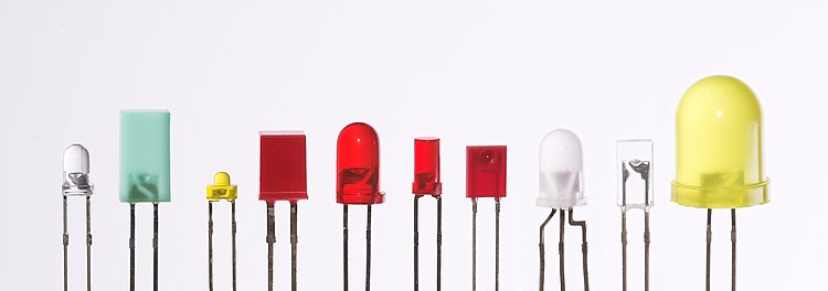
LEDs are produced in a variety of shapes and sizes. The color of the plastic lens is often the same as the actual color of light emitted, but not always. For instance, purple plastic is often used for infrared LEDs, and most blue devices have colorless housings. Modern high-power LEDs such as those used for lighting and backlighting are generally found in surface-mount technology (SMT) packages (not shown).

Automotive applications for LEDs continue to grow.
Energy consumption[edit]
In the US, one kilowatt-hour (3.6 MJ) of electricity currently causes an average 1.34 pounds (610 g) of CO
2 emission.[183] Assuming the average light bulb is on for 10 hours a day, a 40-watt bulb causes 196 pounds (89 kg) of CO
2 emission per year. The 6-watt LED equivalent only causes 30 pounds (14 kg) of CO
2 over the same time span. A building’s carbon footprint from lighting can, therefore, be reduced by 85% by exchanging all incandescent bulbs for new LEDs—if a building previously used only incandescent bulbs.
In practice, most buildings that use a lot of lighting use fluorescent lighting, which has 22% luminous efficiency compared with 5% for filaments, so changing to LED lighting would still give a 34% reduction in electrical power use and carbon emissions.
The reduction in carbon emissions depends on the source of electricity. Nuclear power in the United States produced 19.2% of electricity in 2011, so reducing electricity consumption in the U.S. reduces carbon emissions more than in France (75% nuclear electricity) or Norway (almost entirely hydroelectric).
Replacing lights that spend the most time lit results in the most savings, so LED lights in infrequently used locations bring a smaller return on investment.
Light sources for machine vision systems[edit]
Machine vision systems often require bright and homogeneous illumination, so features of interest are easier to process. LEDs are often used for this purpose, and this is likely to remain one of their major uses until the price drops low enough to make signaling and illumination uses more widespread. Barcode scanners are the most common example of machine vision, and many low-cost products use red LEDs instead of lasers.[184] Optical computer mice are an example of LEDs in machine vision, as it is used to provide an even light source on the surface for the miniature camera within the mouse. LEDs constitute a nearly ideal light source for machine vision systems for several reasons:
- The size of the illuminated field is usually comparatively small and machine vision systems are often quite expensive, so the cost of the light source is usually a minor concern. However, it might not be easy to replace a broken light source placed within complex machinery, and here the long service life of LEDs is a benefit.
- LED elements tend to be small and can be placed with high density over flat or even-shaped substrates (PCBs etc.) so that bright and homogeneous sources that direct light from tightly controlled directions on inspected parts can be designed. This can often be obtained with small, low-cost lenses and diffusers, helping to achieve high light densities with control over lighting levels and homogeneity. LED sources can be shaped in several configurations (spot lights for reflective illumination; ring lights for coaxial illumination; backlights for contour illumination; linear assemblies; flat, large format panels; dome sources for diffused, omnidirectional illumination).
- LEDs can be easily strobed (in the microsecond range and below) and synchronized with imaging. High-power LEDs are available allowing well-lit images even with very short light pulses. This is often used to obtain crisp and sharp "still" images of quickly moving parts.
- LEDs come in several different colors and wavelengths, allowing easy use of the best color for each need, where different color may provide better visibility of features of interest. Having a precisely known spectrum lets tightly matched filters be used to separate informative bandwidth or to reduce disturbing effects of ambient light. LEDs usually operate at comparatively low working temperatures, simplifying heat management, and dissipation. This allows using plastic lenses, filters, and diffusers. Waterproof units can also easily be designed, allowing use in harsh or wet environments (food, beverage, oil industries).[184]


Other applications[edit]


The light from LEDs can be modulated very quickly so they are used extensively in optical fiber and free space optics communications. This includes remote controls, such as for TVs, VCRs, and LED Computers, where infrared LEDs are often used. Opto-isolators use an LED combined with a photodiode or phototransistor to provide a signal path with electrical isolation between two circuits. This is especially useful in medical equipment where the signals from a low-voltage sensor circuit (usually battery-powered) in contact with a living organism must be electrically isolated from any possible electrical failure in a recording or monitoring device operating at potentially dangerous voltages. An optoisolator also lets information be transferred between circuits that don't share a common ground potential.
Many sensor systems rely on light as the signal source. LEDs are often ideal as a light source due to the requirements of the sensors. LEDs are used as motion sensors, for example in optical computer mice. The Nintendo Wii's sensor bar uses infrared LEDs. Pulse oximeters use them for measuring oxygen saturation. Some flatbed scanners use arrays of RGB LEDs rather than the typical cold-cathode fluorescent lamp as the light source. Having independent control of three illuminated colors allows the scanner to calibrate itself for more accurate color balance, and there is no need for warm-up. Further, its sensors only need be monochromatic, since at any one time the page being scanned is only lit by one color of light. Since LEDs can also be used as photodiodes, they can be used for both photo emission and detection. This could be used, for example, in a touchscreen that registers reflected light from a finger or stylus.[185] Many materials and biological systems are sensitive to, or dependent on, light. Grow lights use LEDs to increase photosynthesis in plants,[186] and bacteria and viruses can be removed from water and other substances using UV LEDs for sterilization.[100]
LEDs have also been used as a medium-quality voltage reference in electronic circuits. The forward voltage drop (e.g. about 1.7 V for a normal red LED) can be used instead of a Zener diode in low-voltage regulators. Red LEDs have the flattest I/V curve above the knee. Nitride-based LEDs have a fairly steep I/V curve and are useless for this purpose. Although LED forward voltage is far more current-dependent than a Zener diode, Zener diodes with breakdown voltages below 3 V are not widely available.
The progressive miniaturization of low-voltage lighting technology, such as LEDs and OLEDs, suitable to incorporate into low-thickness materials has fostered experimentation in combining light sources and wall covering surfaces for interior walls.[187] The new possibilities offered by these developments have prompted some designers and companies, such as Meystyle,[188] Ingo Maurer,[189] Lomox[190] and Philips,[191] to research and develop proprietary LED wallpaper technologies, some of which are currently available for commercial purchase. Other solutions mainly exist as prototypes or are in the process of being further refined.
Fuses to LED _____ ;;
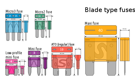
Blade type fuses come in six physical sizes: micro2, micro3, low-profile mini, mini, regular and maxi
Automotive fuses are used to protect the wiring and electrical equipment for vehicles. There are several different types of automotive fuses and their usage is dependent upon the specific application, voltage, and current demands of the electrical circuit. Automotive fuses can be mounted in fuse blocks, inline fuse holders, or fuse clips. Some automotive fuses are occasionally used in non-automotive electrical applications. Standards for automotive fuses are published by SAE International (formerly known as the Society of Automotive Engineers).
Automotive fuses can be classified into four distinct categories:
- Blade fuses
- Glass tube or Bosch type
- Fusible links
- Fuse limiters
Most automotive fuses rated at 32 volts are used on circuits rated 24 volts DC and below. Some vehicles use a dual 12/42 V DC electrical system[9] that will require a fuse rated at 58 V DC.
+++++++++++++++++++++++++++++++++++++++++++++++++++++++++++++
M O D E R N F U S E S TO M O D E R N L E D
nC^r E = h V ignore E = m C^2
+++++++++++++++++++++++++++++++++++++++++++++++++++++++++++++
Tidak ada komentar:
Posting Komentar