Switch Types
An electrical switch is any device used to interrupt the flow of electrons in a circuit. Switches are essentially binary devices: they are either completely on (“closed”) or completely off (“open”). There are many different types of switches, and we will explore some of these types in this chapter.
Though it may seem strange to cover this elementary electrical topic at such a late stage in this book series, I do so because the chapters that follow explore an older realm of digital technology based on mechanical switch contacts rather than solid-state gate circuits, and a thorough understanding of switch types is necessary for the undertaking. Learning the function of switch-based circuits at the same time that you learn about solid-state logic gates makes both topics easier to grasp, and sets the stage for an enhanced learning experience in Boolean algebra, the mathematics behind digital logic circuits.
The simplest type of switch is one where two electrical conductors are brought in contact with each other by the motion of an actuating mechanism. Other switches are more complex, containing electronic circuits able to turn on or off depending on some physical stimulus (such as light or magnetic field) sensed. In any case, the final output of any switch will be (at least) a pair of wire-connection terminals that will either be connected together by the switch’s internal contact mechanism (“closed”), or not connected together (“open”).
Any switch designed to be operated by a person is generally called a hand switch, and they are manufactured in several varieties:

Toggle switches are actuated by a lever angled in one of two or more positions. The common light switch used in household wiring is an example of a toggle switch. Most toggle switches will come to rest in any of their lever positions, while others have an internal spring mechanism returning the lever to a certain normal position, allowing for what is called “momentary” operation.
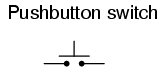
Pushbutton switches are two-position devices actuated with a button that is pressed and released. Most pushbutton switches have an internal spring mechanism returning the button to its “out,” or “unpressed,” position, for momentary operation. Some pushbutton switches will latch alternately on or off with every push of the button. Other pushbutton switches will stay in their “in,” or “pressed,” position until the button is pulled back out. This last type of pushbutton switches usually have a mushroom-shaped button for easy push-pull action.

Selector switches are actuated with a rotary knob or lever of some sort to select one of two or more positions. Like the toggle switch, selector switches can either rest in any of their positions or contain spring-return mechanisms for momentary operation.

A joystick switch is actuated by a lever free to move in more than one axis of motion. One or more of several switch contact mechanisms are actuated depending on which way the lever is pushed, and sometimes by how far it is pushed. The circle-and-dot notation on the switch symbol represents the direction of joystick lever motion required to actuate the contact. Joystick hand switches are commonly used for crane and robot control.
Some switches are specifically designed to be operated by the motion of a machine rather than by the hand of a human operator. These motion-operated switches are commonly called limit switches, because they are often used to limit the motion of a machine by turning off the actuating power to a component if it moves too far. As with hand switches, limit switches come in several varieties:
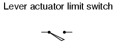
These limit switches closely resemble rugged toggle or selector hand switches fitted with a lever pushed by the machine part. Often, the levers are tipped with a small roller bearing, preventing the lever from being worn off by repeated contact with the machine part.
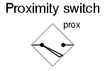
Proximity switches sense the approach of a metallic machine part either by a magnetic or high-frequency electromagnetic field. Simple proximity switches use a permanent magnet to actuate a sealed switch mechanism whenever the machine part gets close (typically 1 inch or less). More complex proximity switches work like a metal detector, energizing a coil of wire with a high-frequency current, and electronically monitoring the magnitude of that current. If a metallic part (not necessarily magnetic) gets close enough to the coil, the current will increase, and trip the monitoring circuit. The symbol shown here for the proximity switch is of the electronic variety, as indicated by the diamond-shaped box surrounding the switch. A non-electronic proximity switch would use the same symbol as the lever-actuated limit switch.
Another form of proximity switch is the optical switch, comprised of a light source and photocell. Machine position is detected by either the interruption or reflection of a light beam. Optical switches are also useful in safety applications, where beams of light can be used to detect personnel entry into a dangerous area.
In many industrial processes, it is necessary to monitor various physical quantities with switches. Such switches can be used to sound alarms, indicating that a process variable has exceeded normal parameters, or they can be used to shut down processes or equipment if those variables have reached dangerous or destructive levels. There are many different types of process switches:

These switches sense the rotary speed of a shaft either by a centrifugal weight mechanism mounted on the shaft, or by some kind of non-contact detection of shaft motion such as optical or magnetic.

Gas or liquid pressure can be used to actuate a switch mechanism if that pressure is applied to a piston, diaphragm, or bellows, which converts pressure to mechanical force.

An inexpensive temperature-sensing mechanism is the “bimetallic strip:” a thin strip of two metals, joined back-to-back, each metal having a different rate of thermal expansion. When the strip heats or cools, differing rates of thermal expansion between the two metals causes it to bend. The bending of the strip can then be used to actuate a switch contact mechanism. Other temperature switches use a brass bulb filled with either a liquid or gas, with a tiny tube connecting the bulb to a pressure-sensing switch. As the bulb is heated, the gas or liquid expands, generating a pressure increase which then actuates the switch mechanism.
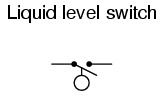
A floating object can be used to actuate a switch mechanism when the liquid level in an tank rises past a certain point. If the liquid is electrically conductive, the liquid itself can be used as a conductor to bridge between two metal probes inserted into the tank at the required depth. The conductivity technique is usually implemented with a special design of relay triggered by a small amount of current through the conductive liquid. In most cases it is impractical and dangerous to switch the full load current of the circuit through a liquid.
Level switches can also be designed to detect the level of solid materials such as wood chips, grain, coal, or animal feed in a storage silo, bin, or hopper. A common design for this application is a small paddle wheel, inserted into the bin at the desired height, which is slowly turned by a small electric motor. When the solid material fills the bin to that height, the material prevents the paddle wheel from turning. The torque response of the small motor than trips the switch mechanism. Another design uses a “tuning fork” shaped metal prong, inserted into the bin from the outside at the desired height. The fork is vibrated at its resonant frequency by an electronic circuit and magnet/electromagnet coil assembly. When the bin fills to that height, the solid material dampens the vibration of the fork, the change in vibration amplitude and/or frequency detected by the electronic circuit.

Inserted into a pipe, a flow switch will detect any gas or liquid flow rate in excess of a certain threshold, usually with a small paddle or vane which is pushed by the flow. Other flow switches are constructed as differential pressure switches, measuring the pressure drop across a restriction built into the pipe.
Another type of level switch, suitable for liquid or solid material detection, is the nuclear switch. Composed of a radioactive source material and a radiation detector, the two are mounted across the diameter of a storage vessel for either solid or liquid material. Any height of material beyond the level of the source/detector arrangement will attenuate the strength of radiation reaching the detector. This decrease in radiation at the detector can be used to trigger a relay mechanism to provide a switch contact for measurement, alarm point, or even control of the vessel level.

Both source and detector are outside of the vessel, with no intrusion at all except the radiation flux itself. The radioactive sources used are fairly weak and pose no immediate health threat to operations or maintenance personnel.
As usual, there is usually more than one way to implement a switch to monitor a physical process or serve as an operator control. There is usually no single “perfect” switch for any application, although some obviously exhibit certain advantages over others. Switches must be intelligently matched to the task for efficient and reliable operation.
Switch Contact Design
A switch can be constructed with any mechanism bringing two conductors into contact with each other in a controlled manner. This can be as simple as allowing two copper wires to touch each other by the motion of a lever, or by directly pushing two metal strips into contact. However, a good switch design must be rugged and reliable, and avoid presenting the operator with the possibility of electric shock. Therefore, industrial switch designs are rarely this crude.
The conductive parts in a switch used to make and break the electrical connection are called contacts. Contacts are typically made of silver or silver-cadmium alloy, whose conductive properties are not significantly compromised by surface corrosion or oxidation. Gold contacts exhibit the best corrosion resistance, but are limited in current-carrying capacity and may “cold weld” if brought together with high mechanical force. Whatever the choice of metal, the switch contacts are guided by a mechanism ensuring square and even contact, for maximum reliability and minimum resistance.
Contacts such as these can be constructed to handle extremely large amounts of electric current, up to thousands of amps in some cases. The limiting factors for switch contact ampacity are as follows:
- Heat generated by current through metal contacts (while closed).
- Sparking caused when contacts are opened or closed.
- The voltage across open switch contacts (potential of current jumping across the gap).
When such environmental concerns exist, other types of contacts can be considered for small switches. These other types of contacts are sealed from contact with the outside air, and therefore do not suffer the same exposure problems that standard contacts do.
A common type of sealed-contact switch is the mercury switch. Mercury is a metallic element, liquid at room temperature. Being a metal, it possesses excellent conductive properties. Being a liquid, it can be brought into contact with metal probes (to close a circuit) inside of a sealed chamber simply by tilting the chamber so that the probes are on the bottom. Many industrial switches use small glass tubes containing mercury which are tilted one way to close the contact, and tilted another way to open. Aside from the problems of tube breakage and spilling mercury (which is a toxic material), and susceptibility to vibration, these devices are an excellent alternative to open-air switch contacts wherever environmental exposure problems are a concern.
Here, a mercury switch (often called a tilt switch) is shown in the open position, where the mercury is out of contact with the two metal contacts at the other end of the glass bulb:

Here, the same switch is shown in the closed position. Gravity now holds the liquid mercury in contact with the two metal contacts, providing electrical continuity from one to the other:

Mercury switch contacts are impractical to build in large sizes, and so you will typically find such contacts rated at no more than a few amps, and no more than 120 volts. There are exceptions, of course, but these are common limits.
Another sealed-contact type of switch is the magnetic reed switch. Like the mercury switch, a reed switch’s contacts are located inside a sealed tube. Unlike the mercury switch which uses liquid metal as the contact medium, the reed switch is simply a pair of very thin, magnetic, metal strips (hence the name “reed”) which are brought into contact with each other by applying a strong magnetic field outside the sealed tube. The source of the magnetic field in this type of switch is usually a permanent magnet, moved closer to or further away from the tube by the actuating mechanism. Due to the small size of the reeds, this type of contact is typically rated at lower currents and voltages than the average mercury switch. However, reed switches typically handle vibration better than mercury contacts, because there is no liquid inside the tube to splash around.
It is common to find general-purpose switch contact voltage and current ratings to be greater on any given switch or relay if the electric power being switched is AC instead of DC. The reason for this is the self-extinguishing tendency of an alternating-current arc across an air gap. Because 60 Hz power line current actually stops and reverses direction 120 times per second, there are many opportunities for the ionized air of an arc to lose enough temperature to stop conducting current, to the point where the arc will not re-start on the next voltage peak. DC, on the other hand, is a continuous, uninterrupted flow of electrons which tends to maintain an arc across an air gap much better. Therefore, switch contacts of any kind incur more wear when switching a given value of direct current than for the same value of alternating current. The problem of switching DC is exaggerated when the load has a significant amount of inductance, as there will be very high voltages generated across the switch’s contacts when the circuit is opened (the inductor doing its best to maintain circuit current at the same magnitude as when the switch was closed).
With both AC and DC, contact arcing can be minimized with the addition of a “snubber” circuit (a capacitor and resistor wired in series) in parallel with the contact, like this:
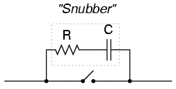
A sudden rise in voltage across the switch contact caused by the contact opening will be tempered by the capacitor’s charging action (the capacitor opposing the increase in voltage by drawing current). The resistor limits the amount of current that the capacitor will discharge through the contact when it closes again. If the resistor were not there, the capacitor might actually make the arcing during contact closure worse than the arcing during contact opening without a capacitor! While this addition to the circuit helps mitigate contact arcing, it is not without disadvantage: a prime consideration is the possibility of a failed (shorted) capacitor/resistor combination providing a path for electrons to flow through the circuit at all times, even when the contact is open and current is not desired. The risk of this failure, and the severity of the resulting consequences must be considered against the increased contact wear (and inevitable contact failure) without the snubber circuit.
The use of snubbers in DC switch circuits is nothing new: automobile manufacturers have been doing this for years on engine ignition systems, minimizing the arcing across the switch contact “points” in the distributor with a small capacitor called a condenser. As any mechanic can tell you, the service life of the distributor’s “points” is directly related to how well the condenser is functioning.
With all this discussion concerning the reduction of switch contact arcing, one might be led to think that less current is always better for a mechanical switch. This, however, is not necessarily so. It has been found that a small amount of periodic arcing can actually be good for the switch contacts, because it keeps the contact faces free from small amounts of dirt and corrosion. If a mechanical switch contact is operated with too little current, the contacts will tend to accumulate excessive resistance and may fail prematurely! This minimum amount of electric current necessary to keep a mechanical switch contact in good health is called the wetting current.
Normally, a switch’s wetting current rating is far below its maximum current rating, and well below its normal operating current load in a properly designed system. However, there are applications where a mechanical switch contact may be required to routinely handle currents below normal wetting current limits (for instance, if a mechanical selector switch needs to open or close a digital logic or analog electronic circuit where the current value is extremely small). In these applications, is it highly recommended that gold-plated switch contacts be specified. Gold is a “noble” metal and does not corrode as other metals will. Such contacts have extremely low wetting current requirements as a result. Normal silver or copper alloy contacts will not provide reliable operation if used in such low-current service!
- The parts of a switch responsible for making and breaking electrical continuity are called the “contacts.” Usually made of corrosion-resistant metal alloy, contacts are made to touch each other by a mechanism which helps maintain proper alignment and spacing.
- Mercury switches use a slug of liquid mercury metal as a moving contact. Sealed in a glass tube, the mercury contact’s spark is sealed from the outside environment, making this type of switch ideally suited for atmospheres potentially harboring explosive vapors.
- Reed switches are another type of sealed-contact device, contact being made by two thin metal “reeds” inside a glass tube, brought together by the influence of an external magnetic field.
- Switch contacts suffer greater duress switching DC than AC. This is primarily due to the self-extinguishing nature of an AC arc.
- A resistor-capacitor network called a “snubber” can be connected in parallel with a switch contact to reduce contact arcing.
- Wetting current is the minimum amount of electric current necessary for a switch contact to carry in order for it to be self-cleaning. Normally this value is far below the switch’s maximum current rating.
Contact “Normal” State and Make/Break Sequence
Any kind of switch contact can be designed so that the contacts “close” (establish continuity) when actuated, or “open” (interrupt continuity) when actuated. For switches that have a spring-return mechanism in them, the direction that the spring returns it to with no applied force is called the normal position. Therefore, contacts that are open in this position are called normally open and contacts that are closed in this position are called normally closed.
For process switches, the normal position, or state, is that which the switch is in when there is no process influence on it. An easy way to figure out the normal condition of a process switch is to consider the state of the switch as it sits on a storage shelf, uninstalled. Here are some examples of “normal” process switch conditions:
- Speed switch: Shaft not turning
- Pressure switch: Zero applied pressure
- Temperature switch: Ambient (room) temperature
- Level switch: Empty tank or bin
- Flow switch: Zero liquid flow
The schematic symbology for switches vary according to the switch’s purpose and actuation. A normally-open switch contact is drawn in such a way as to signify an open connection, ready to close when actuated. Conversely, a normally-closed switch is drawn as a closed connection which will be opened when actuated. Note the following symbols:

There is also a generic symbology for any switch contact, using a pair of vertical lines to represent the contact points in a switch. Normally-open contacts are designated by the lines not touching, while normally-closed contacts are designated with a diagonal line bridging between the two lines. Compare the two:

The switch on the left will close when actuated, and will be open while in the “normal” (unactuated) position. The switch on the right will open when actuated, and is closed in the “normal” (unactuated) position. If switches are designated with these generic symbols, the type of switch usually will be noted in text immediately beside the symbol. Please note that the symbol on the left is not to be confused with that of a capacitor. If a capacitor needs to be represented in a control logic schematic, it will be shown like this:

In standard electronic symbology, the figure shown above is reserved for polarity-sensitive capacitors. In control logic symbology, this capacitor symbol is used for any type of capacitor, even when the capacitor is not polarity sensitive, so as to clearly distinguish it from a normally-open switch contact.
With multiple-position selector switches, another design factor must be considered: that is, the sequence of breaking old connections and making new connections as the switch is moved from position to position, the moving contact touching several stationary contacts in sequence.

The selector switch shown above switches a common contact lever to one of five different positions, to contact wires numbered 1 through 5. The most common configuration of a multi-position switch like this is one where the contact with one position is broken before the contact with the next position is made. This configuration is called break-before-make. To give an example, if the switch were set at position number 3 and slowly turned clockwise, the contact lever would move off of the number 3 position, opening that circuit, move to a position between number 3 and number 4 (both circuit paths open), and then touch position number 4, closing that circuit.
There are applications where it is unacceptable to completely open the circuit attached to the “common” wire at any point in time. For such an application, a make-before-break switch design can be built, in which the movable contact lever actually bridges between two positions of contact (between number 3 and number 4, in the above scenario) as it travels between positions. The compromise here is that the circuit must be able to tolerate switch closures between adjacent position contacts (1 and 2, 2 and 3, 3 and 4, 4 and 5) as the selector knob is turned from position to position. Such a switch is shown here:

When movable contact(s) can be brought into one of several positions with stationary contacts, those positions are sometimes called throws. The number of movable contacts is sometimes called poles. Both selector switches shown above with one moving contact and five stationary contacts would be designated as “single-pole, five-throw” switches.
If two identical single-pole, five-throw switches were mechanically ganged together so that they were actuated by the same mechanism, the whole assembly would be called a “double-pole, five-throw” switch:

Here are a few common switch configurations and their abbreviated designations:


- REVIEW:
- The normal state of a switch is that where it is unactuated. For process switches, this is the condition its in when sitting on a shelf, uninstalled.
- A switch that is open when unactuated is called normally-open. A switch that is closed when unactuated is called normally-closed. Sometimes the terms “normally-open” and “normally-closed” are abbreviated N.O. and N.C., respectively.
- The generic symbology for N.O. and N.C. switch contacts is as follows:
- Multiposition switches can be either break-before-make (most common) or make-before-break.
- The “poles” of a switch refers to the number of moving contacts, while the “throws” of a switch refers to the number of stationary contacts per moving contact.
Contact “Bounce”
When a switch is actuated and contacts touch one another under the force of actuation, they are supposed to establish continuity in a single, crisp moment. Unfortunately, though, switches do not exactly achieve this goal. Due to the mass of the moving contact and any elasticity inherent in the mechanism and/or contact materials, contacts will “bounce” upon closure for a period of milliseconds before coming to a full rest and providing unbroken contact. In many applications, switch bounce is of no consequence: it matters little if a switch controlling an incandescent lamp “bounces” for a few cycles every time it is actuated. Since the lamp’s warm-up time greatly exceeds the bounce period, no irregularity in lamp operation will result.
However, if the switch is used to send a signal to an electronic amplifier or some other circuit with a fast response time, contact bounce may produce very noticeable and undesired effects:
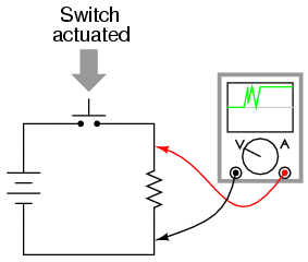
A closer look at the oscilloscope display reveals a rather ugly set of makes and breaks when the switch is actuated a single time:

If, for example, this switch is used to provide a “clock” signal to a digital counter circuit, so that each actuation of the pushbutton switch is supposed to increment the counter by a value of 1, what will happen instead is the counter will increment by several counts each time the switch is actuated. Since mechanical switches often interface with digital electronic circuits in modern systems, switch contact bounce is a frequent design consideration. Somehow, the “chattering” produced by bouncing contacts must be eliminated so that the receiving circuit sees a clean, crisp off/on transition:

Switch contacts may be debounced several different ways. The most direct means is to address the problem at its source: the switch itself. Here are some suggestions for designing switch mechanisms for minimum bounce:
- Reduce the kinetic energy of the moving contact. This will reduce the force of impact as it comes to rest on the stationary contact, thus minimizing bounce.
- Use “buffer springs” on the stationary contact(s) so that they are free to recoil and gently absorb the force of impact from the moving contact.
- Design the switch for “wiping” or “sliding” contact rather than direct impact. “Knife” switch designs use sliding contacts.
- Dampen the switch mechanism’s movement using an air or oil “shock absorber” mechanism.
- Use sets of contacts in parallel with each other, each slightly different in mass or contact gap, so that when one is rebounding off the stationary contact, at least one of the others will still be in firm contact.
- “Wet” the contacts with liquid mercury in a sealed environment. After initial contact is made, the surface tension of the mercury will maintain circuit continuity even though the moving contact may bounce off the stationary contact several times.
Each one of these suggestions sacrifices some aspect of switch performance for limited bounce, and so it is impractical to design all switches with limited contact bounce in mind. Alterations made to reduce the kinetic energy of the contact may result in a small open-contact gap or a slow-moving contact, which limits the amount of voltage the switch may handle and the amount of current it may interrupt. Sliding contacts, while non-bouncing, still produce “noise” (irregular current caused by irregular contact resistance when moving), and suffer from more mechanical wear than normal contacts.
Multiple, parallel contacts give less bounce, but only at greater switch complexity and cost. Using mercury to “wet” the contacts is a very effective means of bounce mitigation, but it is unfortunately limited to switch contacts of low ampacity. Also, mercury-wetted contacts are usually limited in mounting position, as gravity may cause the contacts to “bridge” accidently if oriented the wrong way.
If re-designing the switch mechanism is not an option, mechanical switch contacts may be debounced externally, using other circuit components to condition the signal. A low-pass filter circuit attached to the output of the switch, for example, will reduce the voltage/current fluctuations generated by contact bounce:

Switch contacts may be debounced electronically, using hysteretic transistor circuits (circuits that “latch” in either a high or a low state) with built-in time delays (called “one-shot” circuits), or two inputs controlled by a double-throw switch. These hysteretic circuits, called multivibrators, are discussed in detail in a later chapter.
XXX . XXX Finite-state Machine
Feedback is a fascinating engineering principle. It can turn a rather simple device or process into something substantially more complex. We’ve seen the effects of feedback intentionally integrated into circuit designs with some rather astounding effects:
- Comparator + negative feedback—————-> controllable-gain amplifier
- Comparator + positive feedback—————-> comparator with hysteresis
- Combinational logic + positive feedback—> multivibrator
- Measurement system + negative feedback—-> closed-loop control system
Feedback, both positive and negative, has the tendency to add whole new dynamics to the operation of a device or system. Sometimes, these new dynamics find useful application, while other times they are merely interesting. With look-up tables programmed into memory devices, feedback from the data outputs back to the address inputs creates a whole new type of device: the Finite State Machine, or FSM:
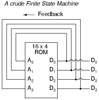
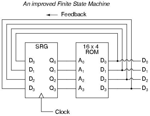
The above circuit illustrates the basic idea: the data stored at each address becomes the next storage location that the ROM gets addressed to. The result is a specific sequence of binary numbers (following the sequence programmed into the ROM) at the output, over time. To avoid signal timing problems, though, we need to connect the data outputs back to the address inputs through a 4-bit D-type flip-flop, so that the sequence takes place step by step to the beat of a controlled clock pulse:
An analogy for the workings of such a device might be an array of post-office boxes, each one with an identifying number on the door (the address), and each one containing a piece of paper with the address of another P.O. box written on it (the data). A person, opening the first P.O. box, would find in it the address of the next P.O. box to open. By storing a particular pattern of addresses in the P.O. boxes, we can dictate the sequence in which each box gets opened, and therefore the sequence of which paper gets read.
Having 16 addressable memory locations in the ROM, this Finite State Machine would have 16 different stable “states” in which it could latch. In each of those states, the identity of the next state would be programmed in to the ROM, awaiting the signal of the next clock pulse to be fed back to the ROM as an address. One useful application of such an FSM would be to generate an arbitrary count sequence, such as Gray Code:
Address  -----> Data          Gray Code count sequence:
0000   -------> 0001                 0   0000
0001   -------> 0011                 1   0001
0010   -------> 0110                 2   0011
0011   -------> 0010                 3   0010
0100   -------> 1100                 4   0110
0101   -------> 0100                 5   0111
0110   -------> 0111                 6   0101
0111   -------> 0101                 7   0100
1000   -------> 0000                 8   1100
1001   -------> 1000                 9   1101
1010   -------> 1011                10   1111
1011   -------> 1001                11   1110
1100   -------> 1101                12   1010
1101   -------> 1111                13   1011
1110   -------> 1010                14   1001
1111   -------> 1110                15   1000
Try to follow the Gray Code count sequence as the FSM would do it: starting at 0000, follow the data stored at that address (0001) to the next address, and so on (0011), and so on (0010), and so on (0110), etc. The result, for the program table shown, is that the sequence of addressing jumps around from address to address in what looks like a haphazard fashion, but when you check each address that is accessed, you will find that it follows the correct order for 4-bit Gray code. When the FSM arrives at its last programmed state (address 1000), the data stored there is 0000, which starts the whole sequence over again at address 0000 in step with the next clock pulse.
We could expand on the capabilities of the above circuit by using a ROM with more address lines, and adding more programming data:
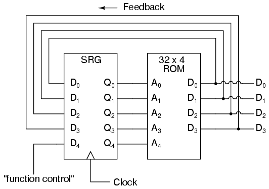
Now, just like the look-up table adder circuit that we turned into an Arithmetic Logic Unit (+, -, x, / functions) by utilizing more address lines as “function control” inputs, this FSM counter can be used to generate more than one count sequence, a different sequence programmed for the four feedback bits (A0 through A3) for each of the two function control line input combinations (A4 = 0 or 1).
Address  -----> Data            Address  -----> Data
00000  -------> 0001            10000  -------> 0001
00001  -------> 0010            10001  -------> 0011
00010  -------> 0011            10010  -------> 0110
00011  -------> 0100            10011  -------> 0010
00100  -------> 0101            10100  -------> 1100
00101  -------> 0110            10101  -------> 0100
00110  -------> 0111            10110  -------> 0111
00111  -------> 1000            10111  -------> 0101
01000  -------> 1001            11000  -------> 0000
01001  -------> 1010            11001  -------> 1000
01010  -------> 1011            11010  -------> 1011
01011  -------> 1100            11011  -------> 1001
01100  -------> 1101            11100  -------> 1101
01101  -------> 1110            11101  -------> 1111
01110  -------> 1111            11110  -------> 1010
01111  -------> 0000            11111  -------> 1110
If A4 is 0, the FSM counts in binary; if A4 is 1, the FSM counts in Gray Code. In either case, the counting sequence is arbitrary: determined by the whim of the programmer. For that matter, the counting sequence doesn’t even have to have 16 steps, as the programmer may decide to have the sequence recycle to 0000 at any one of the steps at all. It is a completely flexible counting device, the behavior strictly determined by the software (programming) in the ROM.
We can expand on the capabilities of the FSM even more by utilizing a ROM chip with additional address input and data output lines. Take the following circuit, for example:
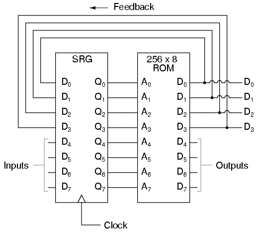
Here, the D0 through D3 data outputs are used exclusively for feedback to the A0 through A3 address lines. Date output lines D4 through D7 can be programmed to output something other than the FSM’s “state” value. Being that four data output bits are being fed back to four address bits, this is still a 16-state device. However, having the output data come from other data output lines gives the programmer more freedom to configure functions than before. In other words, this device can do far more than just count! The programmed output of this FSM is dependent not only upon the state of the feedback address lines (A0 through A3), but also the states of the input lines (A4 through A7). The D-type flip/flop’s clock signal input does not have to come from a pulse generator, either. To make things more interesting, the flip/flop could be wired up to clock on some external event, so that the FSM goes to the next state only when an input signal tells it to.
Now we have a device that better fulfills the meaning of the word “programmable.” The data written to the ROM is a program in the truest sense: the outputs follow a pre-established order based on the inputs to the device and which “step” the device is on in its sequence. This is very close to the operating design of the Turing Machine, a theoretical computing device invented by Alan Turing, mathematically proven to be able to solve any known arithmetic problem, given enough memory capacity.
XXX . XXX Microprocessors ( Auto process switching )
computing device to be really useful, it not only had to be able to generate specific outputs as dictated by programmed instructions, but it also had to be able to write data to memory, and be able to act on that data later. Both the program steps and the processed data were to reside in a common memory “pool,” thus giving way to the label of the stored-program computer. Turing’s theoretical machine utilized a sequential-access tape, which would store data for a control circuit to read, the control circuit re-writing data to the tape and/or moving the tape to a new position to read more data. Modern computers use random-access memory devices instead of sequential-access tapes to accomplish essentially the same thing, except with greater capability.
A helpful illustration is that of early automatic machine tool control technology. Called open-loop, or sometimes just NC (numerical control), these control systems would direct the motion of a machine tool such as a lathe or a mill by following instructions programmed as holes in paper tape. The tape would be run one direction through a “read” mechanism, and the machine would blindly follow the instructions on the tape without regard to any other conditions. While these devices eliminated the burden of having to have a human machinist direct every motion of the machine tool, it was limited in usefulness. Because the machine was blind to the real world, only following the instructions written on the tape, it could not compensate for changing conditions such as expansion of the metal or wear of the mechanisms. Also, the tape programmer had to be acutely aware of the sequence of previous instructions in the machine’s program to avoid troublesome circumstances (such as telling the machine tool to move the drill bit laterally while it is still inserted into a hole in the work), since the device had no memory other than the tape itself, which was read-only. Upgrading from a simple tape reader to a Finite State control design gave the device a sort of memory that could be used to keep track of what it had already done (through feedback of some of the data bits to the address bits), so at least the programmer could decide to have the circuit remember “states” that the machine tool could be in (such as “coolant on,” or tool position). However, there was still room for improvement.
The ultimate approach is to have the program give instructions which would include the writing of new data to a read/write (RAM) memory, which the program could easily recall and process. This way, the control system could record what it had done, and any sensor-detectable process changes, much in the same way that a human machinist might jot down notes or measurements on a scratch-pad for future reference in his or her work. This is what is referred to as CNC, or Closed-loop Numerical Control.
Engineers and computer scientists looked forward to the possibility of building digital devices that could modify their own programming, much the same as the human brain adapts the strength of inter-neural connections depending on environmental experiences (that is why memory retention improves with repeated study, and behavior is modified through consequential feedback). Only if the computer’s program were stored in the same writable memory “pool” as the data would this be practical. It is interesting to note that the notion of a self-modifying program is still considered to be on the cutting edge of computer science. Most computer programming relies on rather fixed sequences of instructions, with a separate field of data being the only information that gets altered.
To facilitate the stored-program approach, we require a device that is much more complex than the simple FSM, although many of the same principles apply. First, we need read/write memory that can be easily accessed: this is easy enough to do. Static or dynamic RAM chips do the job well, and are inexpensive. Secondly, we need some form of logic to process the data stored in memory. Because standard and Boolean arithmetic functions are so useful, we can use an Arithmetic Logic Unit (ALU) such as the look-up table ROM example explored earlier. Finally, we need a device that controls how and where data flows between the memory, the ALU, and the outside world. This so-called Control Unit is the most mysterious piece of the puzzle yet, being comprised of tri-state buffers (to direct data to and from buses) and decoding logic which interprets certain binary codes as instructions to carry out. Sample instructions might be something like: “add the number stored at memory address 0010 with the number stored at memory address 1101,” or, “determine the parity of the data in memory address 0111.” The choice of which binary codes represent which instructions for the Control Unit to decode is largely arbitrary, just as the choice of which binary codes to use in representing the letters of the alphabet in the ASCII standard was largely arbitrary. ASCII, however, is now an internationally recognized standard, whereas control unit instruction codes are almost always manufacturer-specific.
Putting these components together (read/write memory, ALU, and control unit) results in a digital device that is typically called a processor. If minimal memory is used, and all the necessary components are contained on a single integrated circuit, it is called a microprocessor. When combined with the necessary bus-control support circuitry, it is known as a Central Processing Unit, or CPU.
CPU operation is summed up in the so-called fetch/execute cycle. Fetch means to read an instruction from memory for the Control Unit to decode. A small binary counter in the CPU (known as the program counter or instruction pointer) holds the address value where the next instruction is stored in main memory. The Control Unit sends this binary address value to the main memory’s address lines, and the memory’s data output is read by the Control Unit to send to another holding register. If the fetched instruction requires reading more data from memory (for example, in adding two numbers together, we have to read both the numbers that are to be added from main memory or from some other source), the Control Unit appropriately addresses the location of the requested data and directs the data output to ALU registers. Next, the Control Unit would execute the instruction by signaling the ALU to do whatever was requested with the two numbers, and direct the result to another register called the accumulator. The instruction has now been “fetched” and “executed,” so the Control Unit now increments the program counter to step the next instruction, and the cycle repeats itself.
 Microprocessor (CPU)

--------------------------------------
|       ** Program counter **        |
|  (increments address value sent to |
|  external memory chip(s) to fetch  |==========> Address bus
|  the next instruction)             |          (to RAM memory)
--------------------------------------
|        ** Control Unit **          |<=========> Control Bus
|  (decodes instructions read from   | (to all devices sharing
|  program in memory, enables flow   | address and/or data busses;
|  of data to and from ALU, internal | arbitrates all bus communi-
|  registers, and external devices)  | cations)
--------------------------------------
| ** Arithmetic Logic Unit (ALU) **  |
|    (performs all mathematical      |
|     calculations and Boolean       |
|     functions)                     |
--------------------------------------
|          ** Registers **           |
|    (small read/write memories for  |<=========> Data Bus
|     holding instruction codes,     | (from RAM memory and other
|     error codes, ALU data, etc;    |  external devices)
|     includes the "accumulator")    |
--------------------------------------
As one might guess, carrying out even simple instructions is a tedious process. Several steps are necessary for the Control Unit to complete the simplest of mathematical procedures. This is especially true for arithmetic procedures such as exponents, which involve repeated executions (“iterations”) of simpler functions. Just imagine the sheer quantity of steps necessary within the CPU to update the bits of information for the graphic display on a flight simulator game! The only thing which makes such a tedious process practical is the fact that microprocessor circuits are able to repeat the fetch/execute cycle with great speed.
In some microprocessor designs, there are minimal programs stored within a special ROM memory internal to the device (called microcode) which handle all the sub-steps necessary to carry out more complex math operations. This way, only a single instruction has to be read from the program RAM to do the task, and the programmer doesn’t have to deal with trying to tell the microprocessor how to do every minute step. In essence, its a processor inside of a processor; a program running inside of a program.
XXX . XXX Microprocessor Programming
The “vocabulary” of instructions which any particular microprocessor chip possesses is specific to that model of chip. An Intel 80386, for example, uses a completely different set of binary codes than a Motorola 68020, for designating equivalent functions. Unfortunately, there are no standards in place for microprocessor instructions. This makes programming at the very lowest level very confusing and specialized.
When a human programmer develops a set of instructions to directly tell a microprocessor how to do something (like automatically control the fuel injection rate to an engine), they’re programming in the CPU’s own “language.” This language, which consists of the very same binary codes which the Control Unit inside the CPU chip decodes to perform tasks, is often referred to as machine language. While machine language software can be “worded” in binary notation, it is often written in hexadecimal form, because it is easier for human beings to work with. For example, I’ll present just a few of the common instruction codes for the Intel 8080 micro-processor chip:
Hexadecimal    Binary              Instruction description
-----------   --------   -----------------------------------------
|   7B        01111011   Move contents of register A to register E
|
|   87        10000111   Add contents of register A to register D
|
|   1C        00011100   Increment the contents of register E by 1
|
|   D3        11010011   Output byte of data to data bus
Even with hexadecimal notation, these instructions can be easily confused and forgotten. For this purpose, another aid for programmers exists called assembly language. With assembly language, two to four letter mnemonic words are used in place of the actual hex or binary code for describing program steps. For example, the instruction 7B for the Intel 8080 would be “MOV A,E” in assembly language. The mnemonics, of course, are useless to the microprocessor, which can only understand binary codes, but it is an expedient way for programmers to manage the writing of their programs on paper or text editor (word processor). There are even programs written for computers called assemblers which understand these mnemonics, translating them to the appropriate binary codes for a specified target microprocessor, so that the programmer can write a program in the computer’s native language without ever having to deal with strange hex or tedious binary code notation.
Once a program is developed by a person, it must be written into memory before a microprocessor can execute it. If the program is to be stored in ROM (which some are), this can be done with a special machine called a ROM programmer, or (if you’re masochistic), by plugging the ROM chip into a breadboard, powering it up with the appropriate voltages, and writing data by making the right wire connections to the address and data lines, one at a time, for each instruction. If the program is to be stored in volatile memory, such as the operating computer’s RAM memory, there may be a way to type it in by hand through that computer’s keyboard (some computers have a mini-program stored in ROM which tells the microprocessor how to accept keystrokes from a keyboard and store them as commands in RAM), even if it is too dumb to do anything else. Many “hobby” computer kits work like this. If the computer to be programmed is a fully-functional personal computer with an operating system, disk drives, and the whole works, you can simply command the assembler to store your finished program onto a disk for later retrieval. To “run” your program, you would simply type your program’s filename at the prompt, press the Enter key, and the microprocessor’s Program Counter register would be set to point to the location (“address”) on the disk where the first instruction is stored, and your program would run from there.
Although programming in machine language or assembly language makes for fast and highly efficient programs, it takes a lot of time and skill to do so for anything but the simplest tasks, because each machine language instruction is so crude. The answer to this is to develop ways for programmers to write in “high level” languages, which can more efficiently express human thought. Instead of typing in dozens of cryptic assembly language codes, a programmer writing in a high-level language would be able to write something like this . . .
Print "Hello, world!"
. . . and expect the computer to print “Hello, world!” with no further instruction on how to do so. This is a great idea, but how does a microprocessor understand such “human” thinking when its vocabulary is so limited?
The answer comes in two different forms: interpretation, or compilation. Just like two people speaking different languages, there has to be some way to transcend the language barrier in order for them to converse. A translator is needed to translate each person’s words to the other person’s language, one way at a time. For the microprocessor, this means another program, written by another programmer in machine language, which recognizes the ASCII character patterns of high-level commands such as Print (P-r-i-n-t) and can translate them into the necessary bite-size steps that the microprocessor can directly understand. If this translation is done during program execution, just like a translator intervening between two people in a live conversation, it is called “interpretation.” On the other hand, if the entire program is translated to machine language in one fell swoop, like a translator recording a monologue on paper and then translating all the words at one sitting into a written document in the other language, the process is called “compilation.”
Interpretation is simple, but makes for a slow-running program because the microprocessor has to continually translate the program between steps, and that takes time. Compilation takes time initially to translate the whole program into machine code, but the resulting machine code needs no translation after that and runs faster as a consequence. Programming languages such as BASIC and FORTH are interpreted. Languages such as C, C++, FORTRAN, and PASCAL are compiled. Compiled languages are generally considered to be the languages of choice for professional programmers, because of the efficiency of the final product.
Naturally, because machine language vocabularies vary widely from microprocessor to microprocessor, and since high-level languages are designed to be as universal as possible, the interpreting and compiling programs necessary for language translation must be microprocessor-specific. Development of these interpreters and compilers is a most impressive feat: the people who make these programs most definitely earn their keep, especially when you consider the work they must do to keep their software product current with the rapidly-changing microprocessor models appearing on the market!
To mitigate this difficulty, the trend-setting manufacturers of microprocessor chips (most notably, Intel and Motorola) try to design their new products to be backwardly compatible with their older products. For example, the entire instruction set for the Intel 80386 chip is contained within the latest Pentium IV chips, although the Pentium chips have additional instructions that the 80386 chips lack. What this means is that machine-language programs (compilers, too) written for 80386 computers will run on the latest and greatest Intel Pentium IV CPU, but machine-language programs written specifically to take advantage of the Pentium’s larger instruction set will not run on an 80386, because the older CPU simply doesn’t have some of those instructions in its vocabulary: the Control Unit inside the 80386 cannot decode them.
Building on this theme, most compilers have settings that allow the programmer to select which CPU type he or she wants to compile machine-language code for. If they select the 80386 setting, the compiler will perform the translation using only instructions known to the 80386 chip; if they select the Pentium setting, the compiler is free to make use of all instructions known to Pentiums. This is analogous to telling a translator what minimum reading level their audience will be: a document translated for a child will be understandable to an adult, but a document translated for an adult may very well be gibberish to a child .
XXX . XXX Triggering device in programing electronics digitally
In many of industrial operations, the delivery of a variable and controlled amount of electrical power is necessary. The most common of these operations include electric lighting, electric motor speed control, electric welding, and electric heating. Although it is always possible to control the amount of electrical power delivered to a load by using a variable transformer to create a variable secondary output voltage, these transformers are physically large and expensive and need frequent maintenance (in high power ratings). There are other methods of controlling power to a load, but they are mostly not available for high power applications.
Since 1961, an alternative method, using thyristors, has been in use. Both silicon-controlled rectifiers (SCR) and TRIACs are members of the thyristor family. The term thyristor includes all the semiconductor devices, which show inherent ON-OFF behavior, as opposed to allowing gradual changes in conduction. All thyristors are regenerative switching devices, and they cannot operate in linear manner. Thus, a transistor is not a thyristor even though it can operate like a switch (ON-OFF). The transistor is not inherently an ON-OFF device, and it is possible for a transistor to operate linearly.
Some thyristors can be gated into the ON state. Other thyristors cannot be gated ON, but they can be turned ON when the applied voltage reaches a certain breakover value.
XXX . XXX Schmitt trigger
In electronics, a Schmitt trigger is a comparator circuit with hysteresis implemented by applying positive feedback to the noninverting input of a comparator or differential amplifier. It is an active circuit which converts an analog input signal to a digital output signal. The circuit is named a "trigger" because the output retains its value until the input changes sufficiently to trigger a change. In the non-inverting configuration, when the input is higher than a chosen threshold, the output is high. When the input is below a different (lower) chosen threshold the output is low, and when the input is between the two levels the output retains its value. This dual threshold action is called hysteresis and implies that the Schmitt trigger possesses memory and can act as a bistable multivibrator (latch or flip-flop). There is a close relation between the two kinds of circuits: a Schmitt trigger can be converted into a latch and a latch can be converted into a Schmitt trigger.
Schmitt trigger devices are typically used in signal conditioning applications to remove noise from signals used in digital circuits, particularly mechanical contact bounce in switches. They are also used in closed loop negative feedback configurations to implement relaxation oscillators, used in function generators and switching power supplies.

Transfer function of a Schmitt trigger. The horizontal and vertical axes are input voltage and output voltage, respectively. T and −T are the switching thresholds, and M and −M are the output voltage levels.

Comparison of the action of an ordinary comparator and a Schmitt trigger on a noisy analog input signal (U). The output of the comparator is A and the output of the Schmitt trigger is B. The green dotted lines are the circuit's switching thresholds. The Schmitt trigger tends to remove noise from the signal.
The Schmitt trigger was invented by American scientist Otto H. Schmitt in 1934 while he was a graduate student,[1] later described in his doctoral dissertation (1937) as a "thermionic trigger."[2] It was a direct result of Schmitt's study of the neural impulse propagation in squid nerves.[2]
Implementation
Fundamental idea[

Block diagram of a Schmitt trigger circuit. It is a system with positive feedback in which the output signal fed back into the input causes the amplifier A to switch rapidly from one saturated state to the other when the input crosses a threshold.
A > 1 is the amplifier gain
B < 1 is the feedback transfer function
A > 1 is the amplifier gain
B < 1 is the feedback transfer function
Dynamic threshold (series feedback): when the input voltage crosses the threshold in some direction the circuit itself changes its own threshold to the opposite direction. For this purpose, it subtracts a part of its output voltage from the threshold (it is equal to adding voltage to the input voltage). Thus the output affects the threshold and does not impact on the input voltage. These circuits are implemented by a differential amplifier with 'series positive feedback' where the input is connected to the inverting input and the output - to the non-inverting input. In this arrangement, attenuation and summation are separated: a voltage divider acts as an attenuator and the loop acts as a simple series voltage summer. Examples are the classic transistor emitter-coupled Schmitt trigger, the op-amp inverting Schmitt trigger, etc.
Modified input voltage (parallel feedback): when the input voltage crosses the threshold in some direction the circuit changes its input voltage in the same direction (now it adds a part of its output voltage directly to the input voltage). Thus the output augments the input voltage and does not affect the threshold. These circuits can be implemented by a single-ended non-inverting amplifier with 'parallel positive feedback' where the input and the output sources are connected through resistors to the input. The two resistors form a weighted parallel summer incorporating both the attenuation and summation. Examples are the less familiar collector-base coupled Schmitt trigger, the op-amp non-inverting Schmitt trigger, etc.
Some circuits and elements exhibiting negative resistance can also act in a similar way: negative impedance converters (NIC), neon lamps, tunnel diodes (e.g., a diode with an "N"-shaped current–voltage characteristic in the first quadrant), etc. In the last case, an oscillating input will cause the diode to move from one rising leg of the "N" to the other and back again as the input crosses the rising and falling switching thresholds.
Two different unidirectional thresholds are assigned in this case to two separate open-loop comparators (without hysteresis) driving a bistable multivibrator (latch) or flip-flop). The trigger is toggled high when the input voltage crosses down to up the high threshold and low when the input voltage crosses up to down the low threshold. Again, there is a positive feedback but now it is concentrated only in the memory cell. Examples are the 555 timer and the switch debounce circuit.[3]

A symbol of Schmitt trigger shown with a non-inverting hysteresis curve embedded in a buffer. Schmitt triggers can also be shown with inverting hysteresis curves and may be followed by bubbles. The documentation for the particular Schmitt trigger being used must be consulted to determine whether the device is non-inverting (i.e., where positive output transitions are caused by positive-going inputs) or inverting (i.e., where positive output transitions are caused by negative-going inputs).
Transistor Schmitt triggers
Classic emitter-coupled circuit
The original Schmitt trigger is based on the dynamic threshold idea that is implemented by a voltage divider with a switchable upper leg (the collector resistors RC1 and RC2) and a steady lower leg (RE). Q1 acts as a comparator with a differential input (Q1 base-emitter junction) consisting of an inverting (Q1 base) and a non-inverting (Q1 emitter) inputs. The input voltage is applied to the inverting input; the output voltage of the voltage divider is applied to the non-inverting input thus determining its threshold. The comparator output drives the second common collector stage Q2 (an emitter follower) through the voltage divider R1-R2. The emitter-coupled transistors Q1 and Q2 actually compose an electronic double throw switch that switches over the upper legs of the voltage divider and changes the threshold in a different (to the input voltage) direction.This configuration can be considered as a differential amplifier with series positive feedback between its non-inverting input (Q2 base) and output (Q1 collector) that forces the transition process. There is also a smaller negative feedback introduced by the emitter resistor RE. To make the positive feedback dominate over the negative one and to obtain a hysteresis, the proportion between the two collector resistors is chosen RC1 > RC2. Thus less current flows through and less voltage drop is across RE when Q1 is switched on than in the case when Q2 is switched on. As a result, the circuit has two different thresholds in regard to ground (V− in the image).
Operation
Initial state. For the NPN transistors shown on the right, imagine the input voltage is below the shared emitter voltage (high threshold for concreteness) so that Q1 base-emitter junction is reverse-biased and Q1 does not conduct. The Q2 base voltage is determined by the mentioned divider so that Q2 is conducting and the trigger output is in the low state. The two resistors RC2 and RE form another voltage divider that determines the high threshold. Neglecting VBE, the high threshold value is approximately- .

Crossing up the high threshold. When the input voltage (Q1 base voltage) rises slightly above the voltage across the emitter resistor RE (the high threshold), Q1 begins conducting. Its collector voltage goes down and Q2 begins going cut-off, because the voltage divider now provides lower Q2 base voltage. The common emitter voltage follows this change and goes down thus making Q1 conduct more. The current begins steering from the right leg of the circuit to the left one. Although Q1 is more conducting, it passes less current through RE (since RC1 > RC2); the emitter voltage continues dropping and the effective Q1 base-emitter voltage continuously increases. This avalanche-like process continues until Q1 becomes completely turned on (saturated) and Q2 turned off. The trigger is transitioned to the high state and the output (Q2 collector) voltage is close to V+. Now, the two resistors RC1 and RE form a voltage divider that determines the low threshold. Its value is approximately
- .

Variations

Symbol depicting an inverting Schmitt trigger by showing an inverted hysteresis curve inside a buffer. Other symbols show a hysteresis curve (which may be inverting or non-inverting) embedded in a buffer followed by a bubble, which is similar to the traditional symbol for a digital inverter that shows a buffer followed by a bubble. In general, the direction of the Schmitt trigger (inverting or non-inverting) is not necessarily clear from the symbol because multiple conventions are used, even with the same manufacturer. There are several factors leading to such ambiguity,[nb 1] These circumstances may warrant a closer investigation of the documentation for each particular Schmitt trigger.
Direct-coupled circuit. To simplify the circuit, the R1–R2 voltage divider can be omitted connecting Q1 collector directly to Q2 base. The base resistor RB can be omitted as well so that the input voltage source drives directly Q1's base.[4] In this case, the common emitter voltage and Q1 collector voltage are not suitable for outputs. Only Q2 collector should be used as an output since, when the input voltage exceeds the high threshold and Q1 saturates, its base-emitter junction is forward biased and transfers the input voltage variations directly to the emitters. As a result, the common emitter voltage and Q1 collector voltage follow the input voltage. This situation is typical for over-driven transistor differential amplifiers and ECL gates.
Collector-base coupled circuit

Comparison between emitter- and collector-coupled circuit
The emitter-coupled version has the advantage that the input transistor is backward-biased when the input voltage is quite below the high threshold so the transistor is surely cut-off. It was important when germanium transistors were used for implementing the circuit and this advantage has determined its popularity. The input base resistor can be omitted since the emitter resistor limits the current when the input base-emitter junction is forward-biased.The emitter-coupled Schmitt trigger has not low enough level at output logical zero and needs an additional output shifting circuit. The collector-coupled Schmitt trigger has extremely low (almost zero) output level at output logical zero.
Op-amp implementations
Schmitt triggers are commonly implemented using an operational amplifier or a dedicated comparator.[nb 2] An open-loop op-amp and comparator may be considered as an analog-digital device having analog inputs and a digital output that extracts the sign of the voltage difference between its two inputs.[nb 3] The positive feedback is applied by adding a part of the output voltage to the input voltage in series or parallel manner. Due to the extremely high op-amp gain, the loop gain is also high enough and provides the avalanche-like process.Non-inverting Schmitt trigger
In this circuit, the two resistors R1 and R2 form a parallel voltage summer. It adds a part of the output voltage to the input voltage thus augmenting it during and after switching that occurs when the resulting voltage is near ground. This parallel positive feedback creates the needed hysteresis that is controlled by the proportion between the resistances of R1 and R2. The output of the parallel voltage summer is single-ended (it produces voltage with respect to ground) so the circuit does not need an amplifier with a differential input. Since conventional op-amps have a differential input, the inverting input is grounded to make the reference point zero volts.
The output voltage always has the same sign as the op-amp input voltage but it does not always have the same sign as the circuit input voltage (the signs of the two input voltages can differ). When the circuit input voltage is above the high threshold or below the low threshold, the output voltage has the same sign as the circuit input voltage (the circuit is non-inverting). It acts like a comparator that switches at a different point depending on whether the output of the comparator is high or low. When the circuit input voltage is between the thresholds, the output voltage is undefined and it depends on the last state (the circuit behaves as an elementary latch).
Typical transfer function of a non-inverting Schmidt trigger like the circuit above.


A unique property of circuits with parallel positive feedback is the impact on the input source.[citation needed] In circuits with negative parallel feedback (e.g., an inverting amplifier), the virtual ground at the inverting input separates the input source from the op-amp output. Here there is no virtual ground, and the steady op-amp output voltage is applied through R1-R2 network to the input source. The op-amp output passes an opposite current through the input source (it injects current into the source when the input voltage is positive and it draws current from the source when it is negative).

A practical Schmitt trigger with precise thresholds is shown in the figure on the right. The transfer characteristic has exactly the same shape of the previous basic configuration, and the threshold values are the same as well. On the other hand, in the previous case, the output voltage was depending on the power supply, while now it is defined by the Zener diodes (which could also be replaced with a single double-anode Zener diode). In this configuration, the output levels can be modified by appropriate choice of Zener diode, and these levels are resistant to power supply fluctuations (i.e., they increase the PSRR of the comparator). The resistor R3 is there to limit the current through the diodes, and the resistor R4 minimizes the input voltage offset caused by the comparator's input leakage currents (see limitations of real op-amps).
Inverting Schmitt trigger
In the inverting version, the attenuation and summation are separated. The two resistors R1 and R2 act only as a "pure" attenuator (voltage divider). The input loop acts as a simple series voltage summer that adds a part of the output voltage in series to the circuit input voltage. This series positive feedback creates the needed hysteresis that is controlled by the proportion between the resistances of R1 and the whole resistance (R1 and R2). The effective voltage applied to the op-amp input is floating so the op-amp must have a differential input.
The circuit is named inverting since the output voltage always has an opposite sign to the input voltage when it is out of the hysteresis cycle (when the input voltage is above the high threshold or below the low threshold). However, if the input voltage is within the hysteresis cycle (between the high and low thresholds), the circuit can be inverting as well as non-inverting. The output voltage is undefined and it depends on the last state so the circuit behaves like an elementary latch.
To compare the two versions, the circuit operation will be considered at the same conditions as above. If the Schmitt trigger is currently in the high state, the output will be at the positive power supply rail (+VS). The output voltage V+ of the voltage divider is:


In contrast with the parallel version, this circuit does not impact on the input source since the source is separated from the voltage divider output by the high op-amp input differential impedance.
In the inverting amplifier voltage drop across resistor (R1) decides the reference voltages i.e.,upper threshold voltage (V+) and lower threshold voltages (V-) for the comparison with input signal applied. These voltages are fixed as the output voltage and resistor values are fixed.
so by changing the drop across (R1) threshold voltages can be varied. By adding a bias voltage in series with resistor (R1) drop across it can be varied, which can change threshold voltages. Desired values of reference voltages can be obtained by varying bias voltage.
The above equations can be modified as

Applications
Schmitt triggers are typically used in open loop configurations for noise immunity and closed loop configurations to implement function generators.- Analog to digital conversion: The Schmitt trigger is effectively a one bit analog to digital converter. When the signal reaches a given level it switches from its low to high state.
- Level detection: The Schmitt trigger circuit is able to provide level detection. When undertaking this application, it is necessary that the hysteresis voltage is taken into account so that the circuit switches on the required voltage.
- Line reception: When running a data line that may have picked up noise into a logic gate it is necessary to ensure that a logic output level is only changed as the data changed and not as a result of spurious noise that may have been picked up. Using a Schmitt trigger broadly enables the peak to peak noise to reach the level of the hysteresis before spurious triggering may occur.
close loop until automatic systematic with trigger timing electron gate
Noise immunity
One application of a Schmitt trigger is to increase the noise immunity in a circuit with only a single input threshold. With only one input threshold, a noisy input signal near that threshold could cause the output to switch rapidly back and forth from noise alone. A noisy Schmitt Trigger input signal near one threshold can cause only one switch in output value, after which it would have to move beyond the other threshold in order to cause another switch.For example, an amplified infrared photodiode may generate an electric signal that switches frequently between its absolute lowest value and its absolute highest value. This signal is then low-pass filtered to form a smooth signal that rises and falls corresponding to the relative amount of time the switching signal is on and off. That filtered output passes to the input of a Schmitt trigger. The net effect is that the output of the Schmitt trigger only passes from low to high after a received infrared signal excites the photodiode for longer than some known delay, and once the Schmitt trigger is high, it only moves low after the infrared signal ceases to excite the photodiode for longer than a similar known delay. Whereas the photodiode is prone to spurious switching due to noise from the environment, the delay added by the filter and Schmitt trigger ensures that the output only switches when there is certainly an input stimulating the device.
Schmitt triggers are common in many switching circuits for similar reasons (e.g., for switch debouncing).
List of IC including input Schmitt triggers

Use as an oscillator


Here, a comparator-based Schmitt trigger is used in its inverting configuration. Additionally, slow negative feedback is added with an integrating RC network. The result, which is shown on the right, is that the output automatically oscillates from VSS to VDD as the capacitor charges from one Schmitt trigger threshold to the other.
XXX . XXX example trigger timing at How to Use a Robot to Record and Transfer Audio Signals
Why?
In a previous article, I presented a straightforward MEMS microphone circuit that can be included in a robot system or just about any other electronics project. If you’re undecided about how exactly to produce your analog audio, start with that article. If you already have a working microphone interface and now you want to sample and analyze the audio data, you’re ready for this article.We all know the advantages of digital data when it comes to processing and storage. But why transfer the data to a PC? Well, the answer is obvious if your goal is simply to record sound and then analyze it or save it for future enjoyment. But what if the goal is in-system processing? PC analysis is valuable even when the end application requires the robot itself to process the audio data—the powerful and user-friendly software available for PCs can help you to develop and fine-tune the algorithms that will eventually be implemented in the robot’s processor.
Sampling and Timing
Once you have a buffered audio signal, there are two main tasks required for getting that audio data to a PC: analog-to-digital conversion and robot-to-PC data transfer.Let’s first look at the analog-to-digital conversion, particularly the timing details involved. The following schematic excerpt shows the microphone circuit and the connection to the EFM8 microcontroller:
And here is the PCB layout, with the microphone output signal highlighted in blue:
Sample Rate
In general, the standard range of audible frequencies is 20 Hz to 20 kHz. That’s a maximum or optimal range; the real range varies greatly from person to person. Furthermore, for many types of sound reproduction, we do not have to represent the entire audible frequency range. For example, reliable voice communication is possible when the audio signals are restricted to frequencies below 4 kHz, and an upper limit of 10 kHz allows for decent (not great) music reproduction. A standard sampling rate for good-quality audio is 44.1 kHz—just enough to support frequencies up to 20 kHz.My point here is that you are not bound to a 20 kHz bandwidth. You choose the bandwidth according to the audio quality that you want, then you configure your ADC for a sample rate that is about twice as high as the bandwidth. I’m running my 14-bit EFM8 ADC at 16 kHz, which allows me to capture frequencies up to almost 8 kHz.
Storing vs. Sending
Digital audio may seem like old technology, but audio data still requires a lot of memory in the context of a microcontroller. If you’re sampling at 14 bits and 16 thousand samples per second (i.e., 16 ksps), each second of audio requires 32 thousand bytes of data. If your MCU has only 4 kB of RAM, you’re limited to one-eighth of a second. There’s not much you can do with a 125-millisecond recording.Thus, for this project, we will not store audio data. Instead, we will transfer it to the PC continuously, in real time: as soon as each 14-bit sample is generated by the ADC, we send both bytes out the serial port. You can use the same hardware-plus-software arrangement discussed in this article on incorporating microphones into robotics—i.e., a Pololu USB-to-UART converter board (see photo below) and YAT (“Yet Another Terminal”).
When the transfer is complete, we move the data from YAT to Excel.
Timing Conflict?
The primary concern here is ensuring that both bytes are successfully transferred before a new ADC sample arrives. An ADC running at 16 ksps will generate one sample every 62.5 µs. The UART hardware must transfer 10 bits per byte (8 data bits plus one start bit and one stop bit). That’s 20 bits total, and then we also need a small amount of time for interrupt handling and execution of the necessary instructions. So let’s include some margin and say that 25-bit periods must fit within the 62.5 µs between ADC samples.We’ll increase the baud rate to the closest standard value, which is 460800. The limitations of the EFM8’s divider hardware result in an actual baud rate of 453704. Is that close enough? My conclusion from this article is that UART communication will usually be reliable when the baud rates are not different by more than 3.75%. The difference between 460800 and 453704 is about 1.5%, so it should be fine.
Before we move on, let’s use a debug signal and a scope to confirm that we don’t have a timing conflict.
                    SI_INTERRUPT (ADC0EOC_ISR, ADC0EOC_IRQn)
{
 C2ADAPTER_LEDGRN = HIGH;

 ADC0CN0_ADINT = 0; //clear interrupt flag

 SFRPAGE = 0x00; //this page works for both SBUF0 and ADC0H/L

 SBUF0 = ADC0H;
 while(!SCON0_TI);
 SCON0_TI = 0;

 SBUF0 = ADC0L;
 while(!SCON0_TI);
 SCON0_TI = 0;

 Num_Samples_Sent++;
 if(Num_Samples_Sent == 15999)
 {
  //stop Timer5 (one more conversion will occur)
  SFRPAGE = TIMER5_PAGE;
  TMR5CN0_TR5 = 0;
 }

 C2ADAPTER_LEDGRN = LOW;
}
As you can see, C2ADAPTER_LEDGRN goes high at the beginning of the interrupt routine (i.e., when a new ADC sample becomes available) and low at the end of the interrupt routine, at which point the bytes have been transferred and the processor is ready to start idly waiting for the next sample. The cursors in this first scope capture confirm that the rising edges are separated by ~62.5 µs.
You can already see that there is ample time between the completion of the data transfer and the arrival of the next sample. To be precise, we have 18.8 µs of spare time, which is 30% of the ADC sampling period:
YAT and Excel
The bytes are sent using the code shown above (you can remove the C2ADAPTER_LEDGRN = HIGH and C2ADAPTER_LEDGRN = LOW statements if you want to). You can explore the firmware in detail by looking through the source files and the hardware configuration file:Refer to this article for details on using YAT and Excel. However, be warned that YAT could give you problems if you’re dealing with large quantities of data. Apparently, it doesn’t like having lots of data in the terminal monitor, so the save-to-file technique becomes inconvenient.
An alternative approach is to use a log file, but I had serious difficulties with the logging functionality—so serious that I abandoned YAT and decided to write my own C# serial-port logging software that does exactly what I want. Here it is:
So far it’s working well. I’ll probably continue adding functionality until I have a general-purpose serial-port program that efficiently and reliably does (once again) exactly what I need it to do, and nothing more. I’ll make the logger available for download when I’m confident that it’s stable and can adequately handle error scenarios.
You can use the following link to download my Excel file:
It’s currently arranged for 16,000 audio samples, which corresponds to one second of recording time, and it does the following:
- converts bytes to ADC counts and millivolts
- generates two time-domain plots of the audio data
- performs spectral analysis by calculating and plotting Fast Fourier Transform (FFT) data; click here for instructions on using Excel’s FFT functionality
Summary
We’ve discussed some important details related to the digitization of audio signals, and we used custom hardware in conjunction with Excel to visualize and analyze digital audio data. And I even developed some handy serial-port software along the way—a good reminder that projects don’t always follow the expected route.Gathering and Analyzing a Robot’s Accelerometer Data
An accelerometer can be a valuable addition to a robotics project. This article will show you one approach to generating and analyzing acceleration data.
The Accelerometer
In a previous article I introduced the Romi robot chassis from Pololu and a custom-designed Romi-control PCB. You can use the following link to download the full schematic and the BOM.This PCB includes, among other things, an accelerometer. The part I chose is the ADXL326 from Analog Devices. It’s a three-axis, analog-output device and, from the perspective of the user, it’s not at all complicated. As you can see, few external components are required:
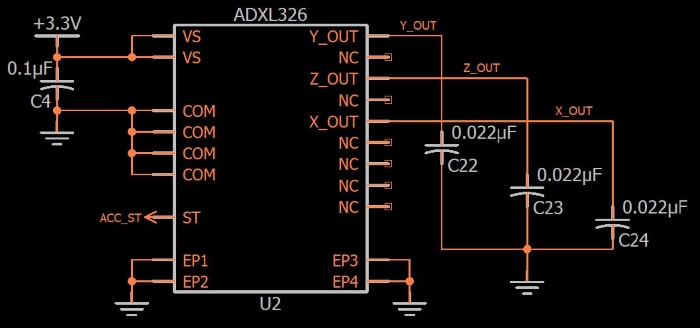
The only real design effort involved is choosing the value of the three output capacitors (C22, C23, and C24). Each of these caps forms a low-pass filter with an internal ~32 kΩ resistor; thus, by choosing an appropriate capacitance value you can limit the bandwidth of the analog outputs according to the needs of your application.
Table taken from the ADXL326 datasheet.
My caps are (nominally) 0.022 µF, so based on the table above my bandwidth will be slightly higher than 200 Hz.
The following diagram conveys the ADXL326’s x, y, and z directions.
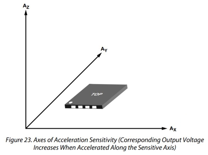
Diagram taken from the ADXL326 datasheet.
The Romi control PCB has the accelerometer oriented as follows:
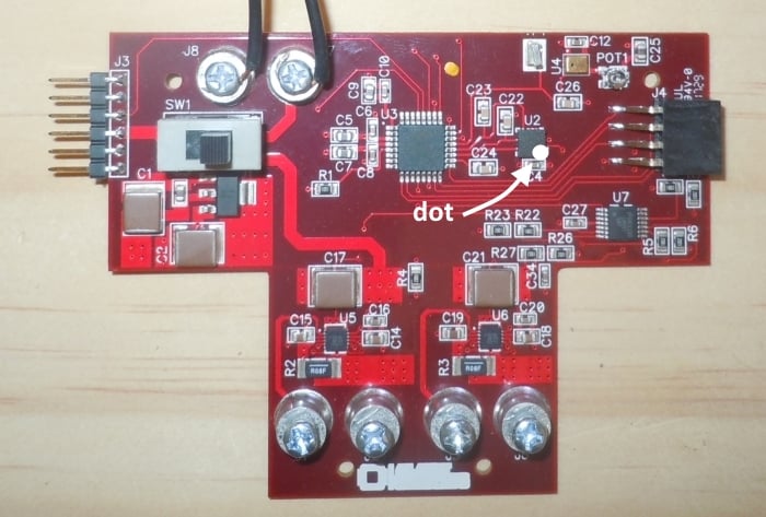
If we combine this orientation with the datasheet diagram and the robot movement directions as defined here, we can determine that
- the robot’s forward direction corresponds to negative x-axis acceleration,
- the reverse direction corresponds to positive x-axis acceleration,
- the rightward direction corresponds to positive y-axis acceleration,
- and the leftward direction corresponds to negative y-axis acceleration.
The ADC
We will use the EFM8’s analog-to-digital converter to digitize the three analog acceleration signals generated by the ADXL326. We’ll use the full 14-bit resolution and the internally generated 2.4 V reference. You can refer to the hardware configuration file and the ADC.c source file for ADC configuration details; these, along with all other source and project files, can be downloaded by clicking the following link:If you look at the full schematic you’ll notice that the accelerometer output signals are connected directly to the ADC inputs. No anti-aliasing filter is needed because bandwidth limitation is accomplished by the low-pass filter discussed above, and I’m pretty sure that we don’t need a voltage follower because the ADC module has a selectable-attenuation module that presumably includes some sort of circuitry that results in low output impedance.
We’ll use the ADC’s autoscan functionality to collect 2400 bytes of ADC data. Each sample requires two bytes and we have three channels (for three axes), and thus we have (2400/2)/3 = 400 samples per axis.
Transferring Data
We need to get the acceleration data to a PC for visualization and analysis. In the past I have used a USB-capable microcontroller in conjunction with a custom Scilab script (see this article, including the links in the “Supporting Information” section). However, I’ve decided to move to a simpler and more versatile system. The previous approach certainly has advantages, but it’s restrictive (because you have to use a microcontroller with USB functionality) and complicated (because of the additional USB firmware and all the Scilab development).The new method relies on YAT (“Yet Another Terminal” program) and Excel. I assume that other spreadsheet software could be used, but the instructions here are specific to Excel.
I appreciate the simplicity of UART communication but computers don’t have serial ports anymore. The simplest remedy to this situation is a USB-to-UART converter; I’m using this one from Pololu. It’s essentially a breakout board for the CP2104 from Silicon Labs; I could design my own but if Pololu sells theirs for $5.95, why bother. This handy little board allows me to write firmware as though USB doesn’t exist—just send a byte, receive a byte, like in the good old days of RS-232.The following photo shows the Romi control PCB connected to the C2 adapter board on the right and the USB-to-UART converter on the left.
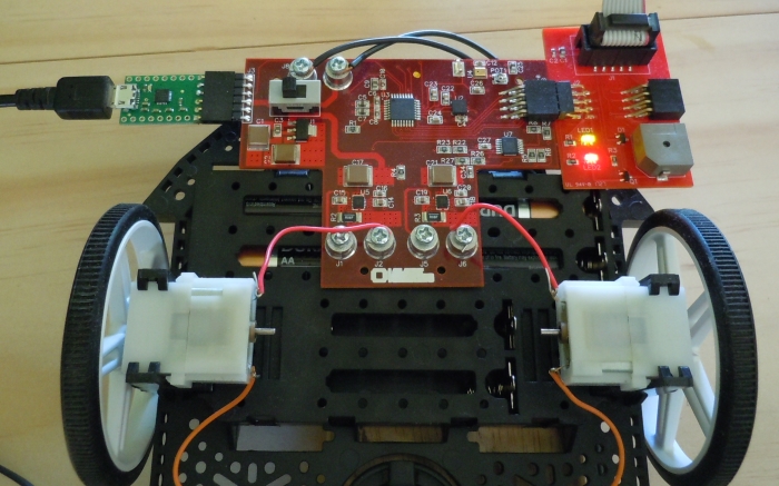
Note: If you’re powering the board from USB, you should ensure that your code doesn’t allow the motors to be enabled. USB ports aren’t designed for that sort of current draw. I recommend physically disconnecting the motors, just to be sure.
When the ADC has finished the 1200 samples (400 per axis), we simply write each byte out the serial port, as follows:
                    void Transfer_ADCBuffer(unsigned int num_bytes)
{
 unsigned int n;

 SFRPAGE = UART0_PAGE;

 SCON0_TI = 0; //make sure that the transmit interrupt flag is cleared

 for(n=0; n<num_bytes; n++)
 {
  SBUF0 = AutoScan_Memory[n];
  while(!SCON0_TI);
  SCON0_TI = 0;
 }
}
The ADC is configured to sequentially sample from P1.5, then P1.6, then P1.7, back to P1.5, and so forth.
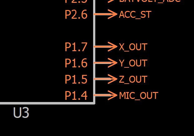
As you can see from the schematic, this results in data that is arranged in memory as follows: z-axis, y-axis, x-axis, z-axis, y-axis, x-axis, and so forth. The ADC is configured for big endian, which means that each sample will begin with the high byte. Thus, our memory looks like this:
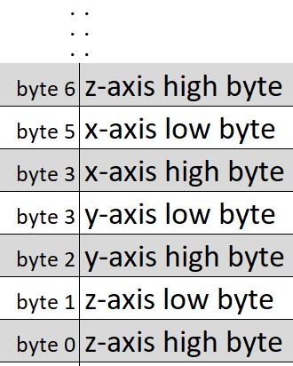
YAT
If everything is working correctly, the ADC data will appear in the YAT window. Here is what you need to do to make it very easy to inspect this data and work with it in Excel:- Go to Terminal->Settings and select “Binary” for “Terminal Type.”
- In the same window, click “Binary Settings”; check the box for “Separate settings for Tx and Rx” then enter “6” for “Break lines after” in the “Rx” section.
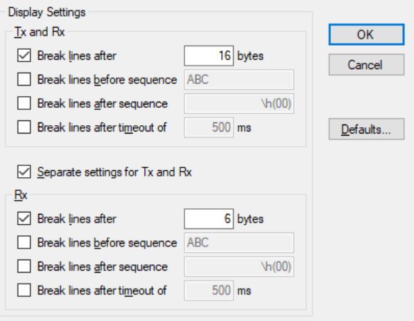
- Back in the main window, click on the “10” button so that the data appears as decimal
Now when you transfer the data, it will appear as follows:
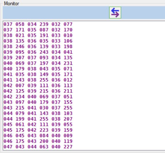
This is the format we want: each row consists of one data point, i.e., one two-byte sample for each acceleration axis.
Excel
First, save the YAT data to a file:
Now you can import this space-separated data into Excel using the “From Text” button in the “Data” ribbon. Note that this block of data will remain “connected” to the data file, so to bring in new data you simply use the “refresh” functionality (see the video below for a demonstration).
Once you have the raw data in Excel, you can convert it to ADC counts and to volts (or millivolts). I have my worksheet set up like this:
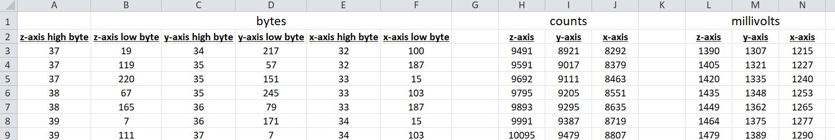
Click to enlarge
On a separate sheet, I have a plot that pulls data from the “millivolts” columns. If you want to use my Excel file, feel free:
Here is a plot of “self-test” output signals (you can read about the self-test functionality in the ADXL326 datasheet).
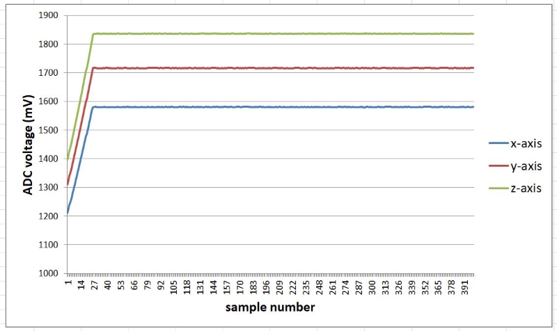
(The initial rising edge is a result of the accelerometer’s startup delay.) Self-test causes the analog outputs to assume a predetermined value; if the measured voltages correspond to the expected voltages, you know that the accelerometer is functional. And because the predetermined value is different for each axis, self-test allows you to confirm that you are associating the samples with the correct axis.
Here are plots for two more data sets. In the first, the PCB is not moving; in the second, I am using my hand to jiggle the robot chassis.
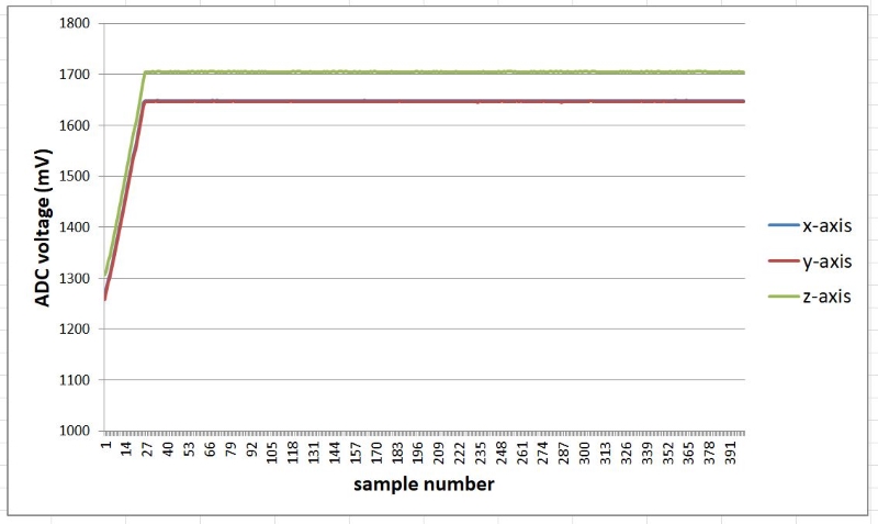

The following video helps to clarify the overall procedure:
Summary
We discussed the hardware implementation of a three-axis, analog-output accelerometer, and I presented a straightforward method of getting stored accelerometer data from the robot’s microcontroller to a PC. We then moved the data into Excel and plotted the results.+++++++++++++++++++++++++++++++++++++++++++++++++++++++++++++++++++++
TRIGGER ELECTRONICS SO WHAT SWITCHING AUTO ELECTRONIC IN CLOSE LOOP
++++++++++++++++++++++++++++++++++++++++++++++++++++++++++++++++++++++
Tidak ada komentar:
Posting Komentar