MARIA PREFER in electronic components traveling a few light years will use photons in future electronic equipment to replace the speed of the switching process and signal conditioner in the form of old electronic components such as silicon and germanium microcontrolers and nanocontrolers AMNIMARJESLOW GOVERMENT SUIT 91220017 Sū-kōnen idō suru denshi buhin wa, shōrai no denshi kiki de kōshi o shiyō shimasu 0209601001 LJBUS SPACE 21 forward 22 -24 ___ Thanks to Lord Jesus ... God who is the father of heaven who is in control with his light he guides our steps to calm water ___ Gen.Mac Tech Zone The Future is light on electronics component for ligh velocity at space ship
An electronic component is any physical entity in an electronic system used to affect the electrons
or their associated fields in a manner consistent with the intended
function of the electronic system. Components are generally intended to
be connected together, usually by being soldered to a printed circuit board (PCB), to create an electronic circuit with a particular function (for example an amplifier, radio receiver, or oscillator). Components may be packaged singly, or in more complex groups as integrated circuits. Some common electronic components are capacitors, inductors, resistors, diodes, transistors, etc. Components are often categorized as active (e.g. transistors and thyristors) or passive (e.g. resistors, diodes, inductors and capacitors ) .
Types of circuits
Circuits
and components can be divided into two groups: analog and digital. A
particular device may consist of circuitry that has one or the other or a
mix of the two types.
Most analog electronic appliances, such as radio receivers, are constructed from combinations of a few types of basic circuits. Analog circuits use a continuous range of voltage or current as opposed to discrete levels as in digital circuits.
The number of different analog circuits so far devised is huge,
especially because a 'circuit' can be defined as anything from a single
component, to systems containing thousands of components.
Analog circuits are sometimes called linear circuits
although many non-linear effects are used in analog circuits such as
mixers, modulators, etc. Good examples of analog circuits include vacuum
tube and transistor amplifiers, operational amplifiers and oscillators.
One rarely finds modern circuits that are entirely analog. These
days analog circuitry may use digital or even microprocessor techniques
to improve performance. This type of circuit is usually called "mixed
signal" rather than analog or digital.
Sometimes it may be difficult to differentiate between analog and
digital circuits as they have elements of both linear and non-linear
operation. An example is the comparator which takes in a continuous
range of voltage but only outputs one of two levels as in a digital
circuit. Similarly, an overdriven transistor amplifier can take on the
characteristics of a controlled switch
having essentially two levels of output. In fact, many digital
circuits are actually implemented as variations of analog circuits
similar to this example – after all, all aspects of the real physical
world are essentially analog, so digital effects are only realized by
constraining analog behavior.
Digital circuits are electric circuits based on a number of discrete
voltage levels. Digital circuits are the most common physical
representation of Boolean algebra,
and are the basis of all digital computers. To most engineers, the
terms "digital circuit", "digital system" and "logic" are
interchangeable in the context of digital circuits.
Most digital circuits use a binary system with two voltage levels
labeled "0" and "1". Often logic "0" will be a lower voltage and
referred to as "Low" while logic "1" is referred to as "High". However,
some systems use the reverse definition ("0" is "High") or are current
based. Quite often the logic designer may reverse these definitions
from one circuit to the next as he sees fit to facilitate his design.
The definition of the levels as "0" or "1" is arbitrary.
Ternary (with three states) logic has been studied, and some prototype computers made.
Computers, electronic clocks, and programmable logic controllers (used to control industrial processes) are constructed of digital circuits. Digital signal processors are another example.
Building blocks:
control loop with AI and Internet for e- Money Transaction
Electronic noise is defined
as unwanted disturbances superposed on a useful signal that tend to
obscure its information content. Noise is not the same as signal
distortion caused by a circuit. Noise is associated with all electronic
circuits. Noise may be electromagnetically or thermally generated, which
can be decreased by lowering the operating temperature of the circuit. Other types of noise, such as shot noise cannot be removed as they are due to limitations in physical properties.
Mathematical methods are integral to the study of electronics. To
become proficient in electronics it is also necessary to become
proficient in the mathematics of circuit analysis.
Circuit analysis is the study of methods of solving generally
linear systems for unknown variables such as the voltage at a certain node or the current through a certain branch of a network. A common analytical tool for this is the SPICE circuit simulator.
Also important to electronics is the study and understanding of electromagnetic field theory.
Due to the complex nature of electronics theory, laboratory
experimentation is an important part of the development of electronic
devices. These experiments are used to test or verify the engineer's
design and detect errors. Historically, electronics labs have consisted
of electronics devices and equipment located in a physical space,
although in more recent years the trend has been towards electronics lab
simulation software, such as CircuitLogix, Multisim, and PSpice.
Many different methods of connecting components have been used over the years. For instance, early electronics often used point to point wiring with components attached to wooden breadboards to construct circuits. Cordwood construction and wire wrap were other methods used. Most modern day electronics now use printed circuit boards made of materials such as FR4, or the cheaper (and less hard-wearing) Synthetic Resin Bonded Paper (SRBP,
also known as Paxoline/Paxolin (trade marks) and FR2) – characterised
by its brown colour. Health and environmental concerns associated with
electronics assembly have gained increased attention in recent years,
especially for products destined to the European Union, with its Restriction of Hazardous Substances Directive (RoHS) and Waste Electrical and Electronic Equipment Directive (WEEE), which went into force in July 2006.
Electronic systems design deals with the multi-disciplinary design issues of complex electronic devices and systems, such as mobile phones and computers. The subject covers a broad spectrum, from the design and development of an electronic system (new product development) to assuring its proper function, service life and disposal. Electronic systems design is therefore the process of defining and developing complex electronic devices to satisfy specified requirements of the user.
Mounting Options
Electrical components are generally mounted in the following ways:
For the past four decades, the electronics industry has been driven by what is called “Moore’s Law,”
which is not a law but more an axiom or observation. Effectively, it
suggests that the electronic devices double in speed and capability
about every two years. And indeed, every year tech companies come up
with new, faster, smarter and better gadgets.
Specifically, Moore’s Law, as articulated by Intel cofounder Gordon
Moore, is that “The number of transistors incorporated in a chip will approximately double every 24 months.”
Transistors, tiny electrical switches, are the fundamental unit that
drives all the electronic gadgets we can think of. As they get smaller,
they also get faster and consume less electricity to operate.
In the technology world, one of the biggest questions of the 21st
century is: How small can we make transistors? If there is a limit to
how tiny they can get, we might reach a point at which we can no longer
continue to make smaller, more powerful, more efficient devices. It’s an
industry with more than US$200 billion in annual revenue in the U.S. alone. Might it stop growing?
Getting close to the limit
At the present, companies like Intel are mass-producing transistors 14 nanometers across – just 14 times wider than DNA molecules. They’re made of silicon, the second-most abundant material on our planet. Silicon’s atomic size is about 0.2 nanometers.
Today’s transistors are about 70 silicon atoms wide, so the
possibility of making them even smaller is itself shrinking. We’re
getting very close to the limit of how small we can make a transistor.
At present, transistors use electrical signals – electrons moving
from one place to another – to communicate. But if we could use light,
made up of photons, instead of electricity, we could make transistors
even faster. My work, on finding ways to integrate light-based
processing with existing chips, is part of that nascent effort.
Putting light inside a chip
A transistor has three parts;
think of them as parts of a digital camera. First, information comes
into the lens, analogous to a transistor’s source. Then it travels
through a channel from the image sensor to the wires inside the camera.
And lastly, the information is stored on the camera’s memory card, which
is called a transistor’s “drain” – where the information ultimately
ends up.
Light waves can have different frequencies.maxhurtz
Right now, all of that happens by moving electrons around. To
substitute light as the medium, we actually need to move photons
instead. Subatomic particles like electrons and photons travel in a wave
motion, vibrating up and down even as they move in one direction. The
length of each wave depends on what it’s traveling through.
In silicon, the most efficient wavelength for photons is 1.3 micrometers. This is very small – a human hair is around 100 micrometers across. But electrons in silicon are even smaller – with wavelengths 50 to 1,000 times shorter than photons.
This means the equipment to handle photons needs to be bigger than
the electron-handling devices we have today. So it might seem like it
would force us to build larger transistors, rather than smaller ones.
However, for two reasons, we could keep chips the same size and
deliver more processing power, shrink chips while providing the same
power, or, potentially both. First, a photonic chip
needs only a few light sources, generating photons that can then be
directed around the chip with very small lenses and mirrors.
And second, light is much faster than electrons. On average photons can travel about 20 times faster
than electrons in a chip. That means computers that are 20 times
faster, a speed increase that would take about 15 years to achieve with
current technology.
Scientists have demonstrated progress toward photonic chips
in recent years. A key challenge is making sure the new light-based
chips can work with all the existing electronic chips. If we’re able to
figure out how to do it – or even to use light-based transistors to
enhance electronic ones – we could see significant performance
improvement.
When can I get a light-based laptop or smartphone?
We still have some way to go before the first consumer device reaches
the market, and progress takes time. The first transistor was made in
the year 1907 using vacuum tubes, which were typically between one and six inches tall
(on average 100 mm). By 1947, the current type of transistor – the one
that’s now just 14 nanometers across – was invented and it was 40 micrometers long
(about 3,000 times longer than the current one). And in 1971 the first
commercial microprocessor (the powerhouse of any electronic gadget) was 1,000 times bigger than today’s when it was released.
The vast research efforts and the consequential evolution seen in the
electronics industry are only starting in the photonic industry. As a
result, current electronics can perform tasks that are far more complex
than the best current photonic devices. But as research proceeds,
light’s capability will catch up to, and ultimately surpass,
electronics’ speeds. However long it takes to get there, the future of
photonics is bright.
The photon is a type of elementary particle. It is the quantum of the electromagnetic field including electromagnetic radiation such as light and radio waves, and the force carrier for the electromagnetic force (even when static via virtual particles). The invariant mass of the photon is zero; it always moves at the speed of light in a vacuum.
Like all elementary particles, photons are currently best explained by quantum mechanics and exhibit wave–particle duality, exhibiting properties of both waves and particles. For example, a single photon may be refracted by a lens and exhibit wave interference with itself, and it can behave as a particle with definite and finite measurable position or momentum, though not both at the same time as per Heisenberg's uncertainty principle.
The photon's wave and quantum qualities are two observable aspects of a
single phenomenon—they cannot be described by any mechanical model;
a representation of this dual property of light that assumes certain
points on the wavefront to be the seat of the energy is not possible.
The quanta in a light wave are not spatially localized.
The modern concept of the photon was developed gradually by Albert Einstein in the early 20th century to explain experimental observations that did not fit the classical wave model
of light. The benefit of the photon model is that it accounts for the
frequency dependence of light's energy, and explains the ability of matter and electromagnetic radiation to be in thermal equilibrium. The photon model accounts for anomalous observations, including the properties of black-body radiation, that others (notably Max Planck) had tried to explain using semiclassical models. In that model, light is described by Maxwell's equations, but material objects emit and absorb light in quantized
amounts (i.e., they change energy only by certain particular discrete
amounts). Although these semiclassical models contributed to the
development of quantum mechanics, many further experimentsbeginning with the phenomenon of Compton scattering of single photons by electrons, validated Einstein's hypothesis that light itself is quantized.[5] In December 1926, American physical chemistGilbert N. Lewis coined the widely adopted name "photon" for these particles in a letter to Nature] After Arthur H. Compton won the Nobel Prize in 1927 for his scattering studies, most scientists accepted that light quanta have an independent existence, and the term "photon" was accepted.
In the Standard Model of particle physics, photons and other elementary particles are described as a necessary consequence of physical laws having a certain symmetry at every point in spacetime. The intrinsic properties of particles, such as charge, mass, and spin, are determined by this gauge symmetry. The photon concept has led to momentous advances in experimental and theoretical physics, including lasers, Bose–Einstein condensation, quantum field theory, and the probabilistic interpretation of quantum mechanics. It has been applied to photochemistry, high-resolution microscopy, and measurements of molecular distances. Recently, photons have been studied as elements of quantum computers, and for applications in optical imaging and optical communication such as quantum cryptography.
Einstein's light quantum
Unlike
Planck, Einstein entertained the possibility that there might be actual
physical quanta of light—what we now call photons. He noticed that a
light quantum with energy proportional to its frequency would explain a
number of troubling puzzles and paradoxes, including an unpublished law
by Stokes, the ultraviolet catastrophe, and the photoelectric effect.
Stokes's law said simply that the frequency of fluorescent light cannot
be greater than the frequency of the light (usually ultraviolet)
inducing it. Einstein eliminated the ultraviolet catastrophe by
imagining a gas of photons behaving like a gas of electrons that he had
previously considered. He was advised by a colleague to be careful how
he wrote up this paper, in order to not challenge Planck, a powerful
figure in physics, too directly, and indeed the warning was justified,
as Planck never forgave him for writing it.
Optics
Optics is the branch of physics that studies the behaviour and properties of light, including its interactions with matter and the construction of instruments that use or detect it. Optics usually describes the behaviour of visible, ultraviolet, and infrared light. Because light is an electromagnetic wave, other forms of electromagnetic radiation such as X-rays, microwaves, and radio waves exhibit similar properties.
Most optical phenomena can be accounted for using the classical electromagnetic
description of light. Complete electromagnetic descriptions of light
are, however, often difficult to apply in practice. Practical optics is
usually done using simplified models. The most common of these, geometric optics, treats light as a collection of rays that travel in straight lines and bend when they pass through or reflect from surfaces. Physical optics is a more comprehensive model of light, which includes wave effects such as diffraction and interference
that cannot be accounted for in geometric optics. Historically, the
ray-based model of light was developed first, followed by the wave model
of light. Progress in electromagnetic theory in the 19th century led to
the discovery that light waves were in fact electromagnetic radiation.
Some phenomena depend on the fact that light has both wave-like and particle-like properties. Explanation of these effects requires quantum mechanics. When considering light's particle-like properties, the light is modelled as a collection of particles called "photons". Quantum optics deals with the application of quantum mechanics to optical systems.
Optical science is relevant to and studied in many related disciplines including astronomy, various engineering fields, photography, and medicine (particularly ophthalmology and optometry). Practical applications of optics are found in a variety of technologies and everyday objects, including mirrors, lenses, telescopes, microscopes, lasers, and fibre optics.
Conceptual
animation of light dispersion through a prism. High frequency (blue)
light is deflected the most, and low frequency (red) the least.
Refractive processes take place in the physical optics limit, where
the wavelength of light is similar to other distances, as a kind of
scattering. The simplest type of scattering is Thomson scattering
which occurs when electromagnetic waves are deflected by single
particles. In the limit of Thomson scattering, in which the wavelike
nature of light is evident, light is dispersed independent of the
frequency, in contrast to Compton scattering which is frequency-dependent and strictly a quantum mechanical
process, involving the nature of light as particles. In a statistical
sense, elastic scattering of light by numerous particles much smaller
than the wavelength of the light is a process known as Rayleigh scattering while the similar process for scattering by particles that are similar or larger in wavelength is known as Mie scattering with the Tyndall effect being a commonly observed result. A small proportion of light scattering from atoms or molecules may undergo Raman scattering, wherein the frequency changes due to excitation of the atoms and molecules. Brillouin scattering occurs when the frequency of light changes due to local changes with time and movements of a dense material.
Dispersion occurs when different frequencies of light have different phase velocities, due either to material properties (material dispersion) or to the geometry of an optical waveguide (waveguide dispersion).
The most familiar form of dispersion is a decrease in index of
refraction with increasing wavelength, which is seen in most transparent
materials. This is called "normal dispersion". It occurs in all dielectric materials, in wavelength ranges where the material does not absorb light.]
In wavelength ranges where a medium has significant absorption, the
index of refraction can increase with wavelength. This is called
"anomalous dispersion".
The separation of colours by a prism is an example of normal
dispersion. At the surfaces of the prism, Snell's law predicts that
light incident at an angle θ to the normal will be refracted at an angle
arcsin(sin (θ) / n). Thus, blue light, with its higher refractive index, is bent more strongly than red light, resulting in the well-known rainbow pattern.
Dispersion: two sinusoids propagating at different speeds make a moving interference pattern. The red dot moves with the phase velocity, and the green dots propagate with the group velocity.
In this case, the phase velocity is twice the group velocity. The red
dot overtakes two green dots, when moving from the left to the right of
the figure. In effect, the individual waves (which travel with the phase
velocity) escape from the wave packet (which travels with the group
velocity).
Material dispersion is often characterised by the Abbe number,
which gives a simple measure of dispersion based on the index of
refraction at three specific wavelengths. Waveguide dispersion is
dependent on the propagation constant.
Both kinds of dispersion cause changes in the group characteristics of
the wave, the features of the wave packet that change with the same
frequency as the amplitude of the electromagnetic wave. "Group velocity
dispersion" manifests as a spreading-out of the signal "envelope" of the
radiation and can be quantified with a group dispersion delay
parameter:
where is the group velocity] For a uniform medium, the group velocity is
where n is the index of refraction and c is the speed of light in a vacuum. This gives a simpler form for the dispersion delay parameter:
If D is less than zero, the medium is said to have positive dispersion or normal dispersion. If D is greater than zero, the medium has negative dispersion.
If a light pulse is propagated through a normally dispersive medium,
the result is the higher frequency components slow down more than the
lower frequency components. The pulse therefore becomes positively chirped, or up-chirped,
increasing in frequency with time. This causes the spectrum coming out
of a prism to appear with red light the least refracted and blue/violet
light the most refracted. Conversely, if a pulse travels through an
anomalously (negatively) dispersive medium, high frequency components
travel faster than the lower ones, and the pulse becomes negatively chirped, or down-chirped, decreasing in frequency with time.
The result of group velocity dispersion, whether negative or
positive, is ultimately temporal spreading of the pulse. This makes
dispersion management extremely important in optical communications
systems based on optical fibres,
since if dispersion is too high, a group of pulses representing
information will each spread in time and merge, making it impossible to
extract the signal.
Polarization is a general property of waves that describes the orientation of their oscillations. For transverse waves
such as many electromagnetic waves, it describes the orientation of the
oscillations in the plane perpendicular to the wave's direction of
travel. The oscillations may be oriented in a single direction (linear polarization), or the oscillation direction may rotate as the wave travels (circular or elliptical polarization).
Circularly polarised waves can rotate rightward or leftward in the
direction of travel, and which of those two rotations is present in a
wave is called the wave's chirality.
The typical way to consider polarization is to keep track of the orientation of the electric field vector
as the electromagnetic wave propagates. The electric field vector of a
plane wave may be arbitrarily divided into two perpendicular components labeled x and y (with z indicating the direction of travel). The shape traced out in the x-y plane by the electric field vector is a Lissajous figure that describes the polarization state]
The following figures show some examples of the evolution of the
electric field vector (blue), with time (the vertical axes), at a
particular point in space, along with its x and y
components (red/left and green/right), and the path traced by the vector
in the plane (purple): The same evolution would occur when looking at
the electric field at a particular time while evolving the point in
space, along the direction opposite to propagation.
Linear
Circular
Elliptical polarization
In the leftmost figure above, the x and y components of the light
wave are in phase. In this case, the ratio of their strengths is
constant, so the direction of the electric vector (the vector sum of
these two components) is constant. Since the tip of the vector traces
out a single line in the plane, this special case is called linear polarization. The direction of this line depends on the relative amplitudes of the two components.
In the middle figure, the two orthogonal components have the same
amplitudes and are 90° out of phase. In this case, one component is
zero when the other component is at maximum or minimum amplitude. There
are two possible phase relationships that satisfy this requirement: the x component can be 90° ahead of the y component or it can be 90° behind the y
component. In this special case, the electric vector traces out a
circle in the plane, so this polarization is called circular
polarization. The rotation direction in the circle depends on which of
the two phase relationships exists and corresponds to right-hand circular polarization and left-hand circular polarization.
In all other cases, where the two components either do not have
the same amplitudes and/or their phase difference is neither zero nor a
multiple of 90°, the polarization is called elliptical polarization because the electric vector traces out an ellipse in the plane (the polarization ellipse). This is shown in the above figure on the right. Detailed mathematics of polarization is done using Jones calculus and is characterised by the Stokes parameters.
Changing polarization
Media that have different indexes of refraction for different polarization modes are called birefringent. Well known manifestations of this effect appear in optical wave plates/retarders (linear modes) and in Faraday rotation/optical rotation (circular modes).
If the path length in the birefringent medium is sufficient, plane
waves will exit the material with a significantly different propagation
direction, due to refraction. For example, this is the case with macroscopic crystals of calcite,
which present the viewer with two offset, orthogonally polarised images
of whatever is viewed through them. It was this effect that provided
the first discovery of polarization, by Erasmus Bartholinus
in 1669. In addition, the phase shift, and thus the change in
polarization state, is usually frequency dependent, which, in
combination with dichroism, often gives rise to bright colours and rainbow-like effects. In mineralogy, such properties, known as pleochroism, are frequently exploited for the purpose of identifying minerals using polarization microscopes. Additionally, many plastics that are not normally birefringent will become so when subject to mechanical stress, a phenomenon which is the basis of photoelasticity] Non-birefringent methods, to rotate the linear polarization of light beams, include the use of prismatic polarization rotators which use total internal reflection in a prism set designed for efficient collinear transmission.
A polariser changing the orientation of linearly polarised light.
In this picture, θ1 – θ0 = θi.
Media that reduce the amplitude of certain polarization modes are called dichroic, with devices that block nearly all of the radiation in one mode known as polarizing filters or simply "polarisers". Malus' law, which is named after Étienne-Louis Malus, says that when a perfect polariser is placed in a linear polarised beam of light, the intensity, I, of the light that passes through is given by
where
I0 is the initial intensity,
and θi is the angle between the light's initial polarization direction and the axis of the polariser.
A beam of unpolarised light can be thought of as containing a uniform
mixture of linear polarizations at all possible angles. Since the
average value of is 1/2, the transmission coefficient becomes
In practice, some light is lost in the polariser and the actual
transmission of unpolarised light will be somewhat lower than this,
around 38% for Polaroid-type polarisers but considerably higher
(>49.9%) for some birefringent prism types.
In addition to birefringence and dichroism in extended media,
polarization effects can also occur at the (reflective) interface
between two materials of different refractive index. These effects are
treated by the Fresnel equations.
Part of the wave is transmitted and part is reflected, with the ratio
depending on angle of incidence and the angle of refraction. In this
way, physical optics recovers Brewster's angle] When light reflects from a thin film
on a surface, interference between the reflections from the film's
surfaces can produce polarization in the reflected and transmitted
light.
Natural light
The effects of a polarising filter
on the sky in a photograph. Left picture is taken without polariser.
For the right picture, filter was adjusted to eliminate certain
polarizations of the scattered blue light from the sky.
Most sources of electromagnetic radiation
contain a large number of atoms or molecules that emit light. The
orientation of the electric fields produced by these emitters may not be
correlated, in which case the light is said to be unpolarised. If there is partial correlation between the emitters, the light is partially polarised.
If the polarization is consistent across the spectrum of the source,
partially polarised light can be described as a superposition of a
completely unpolarised component, and a completely polarised one. One
may then describe the light in terms of the degree of polarization, and the parameters of the polarization ellipse.
Light reflected by shiny transparent materials is partly or fully
polarised, except when the light is normal (perpendicular) to the
surface. It was this effect that allowed the mathematician Étienne-Louis Malus
to make the measurements that allowed for his development of the first
mathematical models for polarised light. Polarization occurs when light
is scattered in the atmosphere. The scattered light produces the brightness and colour in clear skies. This partial polarization of scattered light can be taken advantage of using polarizing filters to darken the sky in photographs. Optical polarization is principally of importance in chemistry due to circular dichroism and optical rotation ("circular birefringence") exhibited by optically active (chiral) molecules .
Modern optics encompasses the areas of optical science and
engineering that became popular in the 20th century. These areas of
optical science typically relate to the electromagnetic or quantum
properties of light but do include other topics. A major subfield of
modern optics, quantum optics,
deals with specifically quantum mechanical properties of light. Quantum
optics is not just theoretical; some modern devices, such as lasers,
have principles of operation that depend on quantum mechanics. Light
detectors, such as photomultipliers and channeltrons, respond to individual photons. Electronic image sensors, such as CCDs, exhibit shot noise corresponding to the statistics of individual photon events. Light-emitting diodes and photovoltaic cells, too, cannot be understood without quantum mechanics. In the study of these devices, quantum optics often overlaps with quantum electronics.
Specialty areas of optics research include the study of how light interacts with specific materials as in crystal optics and metamaterials. Other research focuses on the phenomenology of electromagnetic waves as in singular optics, non-imaging optics, non-linear optics, statistical optics, and radiometry. Additionally, computer engineers have taken an interest in integrated optics, machine vision, and photonic computing as possible components of the "next generation" of computers.
Today, the pure science of optics is called optical science or optical physics to distinguish it from applied optical sciences, which are referred to as optical engineering. Prominent subfields of optical engineering include illumination engineering, photonics, and optoelectronics with practical applications like lens design, fabrication and testing of optical components, and image processing.
Some of these fields overlap, with nebulous boundaries between the
subjects terms that mean slightly different things in different parts of
the world and in different areas of industry. A professional community
of researchers in nonlinear optics has developed in the last several
decades due to advances in laser technology.
Experiments such as this one with high-power lasers are part of the modern optics research.
A laser is a device that emits light (electromagnetic radiation) through a process called stimulated emission. The term laser is an acronym for Light Amplification by Stimulated Emission of Radiation] Laser light is usually spatially coherent, which means that the light either is emitted in a narrow, low-divergence beam, or can be converted into one with the help of optical components such as lenses. Because the microwave equivalent of the laser, the maser, was developed first, devices that emit microwave and radio frequencies are usually called masers.
The Kapitsa–Dirac effect
causes beams of particles to diffract as the result of meeting a
standing wave of light. Light can be used to position matter using
various phenomena (see optical tweezers).
Applications
Optics is part of everyday life. The ubiquity of visual systems in biology indicates the central role optics plays as the science of one of the five senses. Many people benefit from eyeglasses or contact lenses, and optics are integral to the functioning of many consumer goods including cameras. Rainbows and mirages are examples of optical phenomena. Optical communication provides the backbone for both the Internet and modern telephony.
The human eye functions by focusing light onto a layer of photoreceptor cells called the retina,
which forms the inner lining of the back of the eye. The focusing is
accomplished by a series of transparent media. Light entering the eye
passes first through the cornea, which provides much of the eye's optical power. The light then continues through the fluid just behind the cornea—the anterior chamber, then passes through the pupil. The light then passes through the lens,
which focuses the light further and allows adjustment of focus. The
light then passes through the main body of fluid in the eye—the vitreous humour, and reaches the retina. The cells in the retina line the back of the eye, except for where the optic nerve exits; this results in a blind spot.
There are two types of photoreceptor cells, rods and cones, which are sensitive to different aspects of light.Rod cells are sensitive to the intensity of light over a wide frequency range, thus are responsible for black-and-white vision. Rod cells are not present on the fovea,
the area of the retina responsible for central vision, and are not as
responsive as cone cells to spatial and temporal changes in light. There
are, however, twenty times more rod cells than cone cells in the retina
because the rod cells are present across a wider area. Because of their
wider distribution, rods are responsible for peripheral vision.
In contrast, cone cells are less sensitive to the overall
intensity of light, but come in three varieties that are sensitive to
different frequency-ranges and thus are used in the perception of colour and photopic vision.
Cone cells are highly concentrated in the fovea and have a high visual
acuity meaning that they are better at spatial resolution than rod
cells. Since cone cells are not as sensitive to dim light as rod cells,
most night vision
is limited to rod cells. Likewise, since cone cells are in the fovea,
central vision (including the vision needed to do most reading, fine
detail work such as sewing, or careful examination of objects) is done
by cone cells.
Ciliary muscles around the lens allow the eye's focus to be adjusted. This process is known as accommodation. The near point and far point
define the nearest and farthest distances from the eye at which an
object can be brought into sharp focus. For a person with normal vision,
the far point is located at infinity. The near point's location depends
on how much the muscles can increase the curvature of the lens, and how
inflexible the lens has become with age. Optometrists, ophthalmologists, and opticians usually consider an appropriate near point to be closer than normal reading distance—approximately 25 cm.
Defects in vision can be explained using optical principles. As
people age, the lens becomes less flexible and the near point recedes
from the eye, a condition known as presbyopia. Similarly, people suffering from hyperopia
cannot decrease the focal length of their lens enough to allow for
nearby objects to be imaged on their retina. Conversely, people who
cannot increase the focal length of their lens enough to allow for
distant objects to be imaged on the retina suffer from myopia and have a far point that is considerably closer than infinity. A condition known as astigmatism
results when the cornea is not spherical but instead is more curved in
one direction. This causes horizontally extended objects to be focused
on different parts of the retina than vertically extended objects, and
results in distorted images.
All of these conditions can be corrected using corrective lenses. For presbyopia and hyperopia, a converging lens provides the extra curvature necessary to bring the near point closer to the eye while for myopia a diverging lens provides the curvature necessary to send the far point to infinity. Astigmatism is corrected with a cylindrical surface lens that curves more strongly in one direction than in another, compensating for the non-uniformity of the cornea.
The optical power of corrective lenses is measured in diopters, a value equal to the reciprocal
of the focal length measured in metres; with a positive focal length
corresponding to a converging lens and a negative focal length
corresponding to a diverging lens. For lenses that correct for
astigmatism as well, three numbers are given: one for the spherical
power, one for the cylindrical power, and one for the angle of
orientation of the astigmatism.
For the visual effects used in film, video, and computer graphics, see visual effects.
The Ponzo Illusion relies on the fact that parallel lines appear to converge as they approach infinity.
Optical illusions (also called visual illusions) are characterized by visually perceived images that differ from objective reality. The information gathered by the eye is processed in the brain to give a percept
that differs from the object being imaged. Optical illusions can be the
result of a variety of phenomena including physical effects that create
images that are different from the objects that make them, the
physiological effects on the eyes and brain of excessive stimulation
(e.g. brightness, tilt, colour, movement), and cognitive illusions where
the eye and brain make unconscious inferences.[82]
Cognitive illusions include some which result from the
unconscious misapplication of certain optical principles. For example,
the Ames room, Hering, Müller-Lyer, Orbison, Ponzo, Sander, and Wundt illusions
all rely on the suggestion of the appearance of distance by using
converging and diverging lines, in the same way that parallel light rays
(or indeed any set of parallel lines) appear to converge at a vanishing point at infinity in two-dimensionally rendered images with artistic perspective.[83] This suggestion is also responsible for the famous moon illusion where the moon, despite having essentially the same angular size, appears much larger near the horizon than it does at zenith.[84] This illusion so confounded Ptolemy that he incorrectly attributed it to atmospheric refraction when he described it in his treatise, Optics.
Another type of optical illusion exploits broken patterns to
trick the mind into perceiving symmetries or asymmetries that are not
present. Examples include the café wall, Ehrenstein, Fraser spiral, Poggendorff, and Zöllner illusions. Related, but not strictly illusions, are patterns that occur due to the superimposition of periodic structures. For example, transparent tissues with a grid structure produce shapes known as moiré patterns, while the superimposition of periodic transparent patterns comprising parallel opaque lines or curves produces line moiré patterns.
Optical instruments
Illustrations of various optical instruments from the 1728 Cyclopaedia
Single lenses have a variety of applications including photographic lenses, corrective lenses, and magnifying glasses while single mirrors are used in parabolic reflectors and rear-view mirrors.
Combining a number of mirrors, prisms, and lenses produces compound
optical instruments which have practical uses. For example, a periscope
is simply two plane mirrors aligned to allow for viewing around
obstructions. The most famous compound optical instruments in science
are the microscope and the telescope which were both invented by the Dutch in the late 16th century.
Microscopes were first developed with just two lenses: an objective lens and an eyepiece. The objective lens is essentially a magnifying glass and was designed with a very small focal length
while the eyepiece generally has a longer focal length. This has the
effect of producing magnified images of close objects. Generally, an
additional source of illumination is used since magnified images are
dimmer due to the conservation of energy and the spreading of light rays over a larger surface area. Modern microscopes, known as compound microscopes have many lenses in them (typically four) to optimize the functionality and enhance image stability. A slightly different variety of microscope, the comparison microscope, looks at side-by-side images to produce a stereoscopicbinocular view that appears three dimensional when used by humans.
The first telescopes, called refracting telescopes
were also developed with a single objective and eyepiece lens. In
contrast to the microscope, the objective lens of the telescope was
designed with a large focal length to avoid optical aberrations. The
objective focuses an image of a distant object at its focal point which
is adjusted to be at the focal point of an eyepiece of a much smaller
focal length. The main goal of a telescope is not necessarily
magnification, but rather collection of light which is determined by the
physical size of the objective lens. Thus, telescopes are normally
indicated by the diameters of their objectives rather than by the
magnification which can be changed by switching eyepieces. Because the
magnification of a telescope is equal to the focal length of the
objective divided by the focal length of the eyepiece, smaller
focal-length eyepieces cause greater magnification.
Since crafting large lenses is much more difficult than crafting large mirrors, most modern telescopes are reflecting telescopes,
that is, telescopes that use a primary mirror rather than an objective
lens. The same general optical considerations apply to reflecting
telescopes that applied to refracting telescopes, namely, the larger the
primary mirror, the more light collected, and the magnification is
still equal to the focal length of the primary mirror divided by the
focal length of the eyepiece. Professional telescopes generally do not
have eyepieces and instead place an instrument (often a charge-coupled
device) at the focal point instead.
The optics of photography involves both lenses and the medium in which the electromagnetic radiation is recorded, whether it be a plate, film, or charge-coupled device. Photographers must consider the reciprocity of the camera and the shot which is summarized by the relation
In other words, the smaller the aperture (giving greater depth of
focus), the less light coming in, so the length of time has to be
increased (leading to possible blurriness if motion occurs). An example
of the use of the law of reciprocity is the Sunny 16 rule which gives a rough estimate for the settings needed to estimate the proper exposure in daylight.
A camera's aperture is measured by a unitless number called the f-number or f-stop, f/#, often notated as , and given by
where is the focal length, and is the diameter of the entrance pupil. By convention, "f/#" is treated as a single symbol, and specific values of f/# are written by replacing the number sign
with the value. The two ways to increase the f-stop are to either
decrease the diameter of the entrance pupil or change to a longer focal
length (in the case of a zoom lens, this can be done by simply adjusting the lens). Higher f-numbers also have a larger depth of field due to the lens approaching the limit of a pinhole camera which is able to focus all images perfectly, regardless of distance, but requires very long exposure times.
The field of view that the lens will provide changes with the
focal length of the lens. There are three basic classifications based on
the relationship to the diagonal size of the film or sensor size of the
camera to the focal length of the lens:
Normal lens: angle of view of about 50° (called normal because this angle considered roughly equivalent to human vision) and a focal length approximately equal to the diagonal of the film or sensor
Wide-angle lens: angle of view wider than 60° and focal length shorter than a normal lens.
Long focus lens:
angle of view narrower than a normal lens. This is any lens with a
focal length longer than the diagonal measure of the film or sensor. The most common type of long focus lens is the telephoto lens, a design that uses a special telephoto group to be physically shorter than its focal length.
Modern zoom lenses may have some or all of these attributes.
The absolute value for the exposure time required depends on how sensitive to light the medium being used is (measured by the film speed, or, for digital media, by the quantum efficiency).[96]
Early photography used media that had very low light sensitivity, and
so exposure times had to be long even for very bright shots. As
technology has improved, so has the sensitivity through film cameras and
digital cameras.
Other results from physical and geometrical optics apply to
camera optics. For example, the maximum resolution capability of a
particular camera set-up is determined by the diffraction limit associated with the pupil size and given, roughly, by the Rayleigh criterion.
A
colourful sky is often due to scattering of light off particulates and
pollution, as in this photograph of a sunset during the October 2007 California wildfires.
The unique optical properties of the atmosphere cause a wide range of
spectacular optical phenomena. The blue colour of the sky is a direct
result of Rayleigh scattering
which redirects higher frequency (blue) sunlight back into the field of
view of the observer. Because blue light is scattered more easily than
red light, the sun takes on a reddish hue when it is observed through a
thick atmosphere, as during a sunrise or sunset.
Additional particulate matter in the sky can scatter different colours
at different angles creating colourful glowing skies at dusk and dawn.
Scattering off of ice crystals and other particles in the atmosphere are
responsible for halos, afterglows, coronas, rays of sunlight, and sun dogs. The variation in these kinds of phenomena is due to different particle sizes and geometries.
Mirages
are optical phenomena in which light rays are bent due to thermal
variations in the refraction index of air, producing displaced or
heavily distorted images of distant objects. Other dramatic optical
phenomena associated with this include the Novaya Zemlya effect where the sun appears to rise earlier than predicted with a distorted shape. A spectacular form of refraction occurs with a temperature inversion called the Fata Morgana
where objects on the horizon or even beyond the horizon, such as
islands, cliffs, ships or icebergs, appear elongated and elevated, like
"fairy tale castles".
Rainbows
are the result of a combination of internal reflection and dispersive
refraction of light in raindrops. A single reflection off the backs of
an array of raindrops produces a rainbow with an angular size on the sky
that ranges from 40° to 42° with red on the outside. Double rainbows
are produced by two internal reflections with angular size of 50.5° to
54° with violet on the outside. Because rainbows are seen with the sun
180° away from the centre of the rainbow, rainbows are more prominent
the closer the sun is to the horizon
________________________________________
Optical computing
Optical or photonic computing uses photons produced by lasers or diodes for computation. For decades, photons have promised to allow a higher bandwidth than the electrons used in conventional computers.
Most research projects focus on replacing current computer components with optical equivalents, resulting in an optical digital computer system processing binary data.
This approach appears to offer the best short-term prospects for
commercial optical computing, since optical components could be
integrated into traditional computers to produce an optical-electronic
hybrid. However, optoelectronic
devices lose 30% of their energy converting electronic energy into
photons and back; this conversion also slows the transmission of
messages. All-optical computers eliminate the need for
optical-electrical-optical (OEO) conversions, thus lessening the need
for electrical power.
Application-specific devices, such as synthetic aperture radar (SAR) and optical correlators,
have been designed to use the principles of optical computing.
Correlators can be used, for example, to detect and track objects, and to classify serial time-domain optical data
Optical components for binary digital computer
The fundamental building block of modern electronic computers is the transistor. To replace electronic components with optical ones, an equivalent optical transistor is required. This is achieved using materials with a non-linear refractive index. In particular, materials exist
where the intensity of incoming light affects the intensity of the
light transmitted through the material in a similar manner to the
current response of a bipolar transistor. Such an optical transistor can be used to create optical logic gates, which in turn are assembled into the higher level components of the computer's CPU. These will be nonlinear optical crystals used to manipulate light beams into controlling other light beams.
Like any computing system, an Optical computing system needs three things to function well:
optical processor
optical data transfer, e.g. Fiber optic cable
optical storage, e.g. CD/DVD/bluray, etc.
Substituting electrical components will need data format conversion
from photons to electrons, which will make the system slower.
Controversy
There
are disagreements between researchers about the future capabilities of
optical computers; whether or not they may be able to compete with
semiconductor-based electronic computers in terms of speed, power
consumption, cost, and size is an open question. Critics note that real-world logic systems require "logic-level restoration, cascadability, fan-out
and input–output isolation", all of which are currently provided by
electronic transistors at low cost, low power, and high speed. For
optical logic to be competitive beyond a few niche applications, major
breakthroughs in non-linear optical device technology would be required,
or perhaps a change in the nature of computing itself.
Misconceptions, challenges, and prospects
A significant challenge to optical computing is that computation is a nonlinear process in which multiple signals must interact. Light, which is an electromagnetic wave, can only interact with another electromagnetic wave in the presence of electrons in a material,
and the strength of this interaction is much weaker for electromagnetic
waves, such as light, than for the electronic signals in a conventional
computer. This may result in the processing elements for an optical
computer requiring more power and larger dimensions than those for a
conventional electronic computer using transistors.[citation needed]
A further misconception is that since light can travel much faster than the drift velocity of electrons, and at frequencies measured in THz, optical transistors should be capable of extremely high frequencies. However, any electromagnetic wave must obey the transform limit, and therefore the rate at which an optical transistor can respond to a signal is still limited by its spectral bandwidth. However, in fiber optic communications, practical limits such as dispersion often constrain channels
to bandwidths of 10s of GHz, only slightly better than many silicon
transistors. Obtaining dramatically faster operation than electronic
transistors would therefore require practical methods of transmitting ultrashort pulses down highly dispersive waveguides.
Photonic logic
Realization of a photonic controlled-NOT gate for use in quantum computing
Photonic logic is the use of photons (light) in logic gates (NOT, AND, OR, NAND, NOR, XOR, XNOR). Switching is obtained using nonlinear optical effects when two or more signals are combined.
Resonators are especially useful in photonic logic, since they allow a build-up of energy from constructive interference, thus enhancing optical nonlinear effects.
Other approaches that have been investigated include photonic logic at a molecular level, using photoluminescent chemicals. In a demonstration, Witlicki et al. performed logical operations using molecules and SERS.
Unconventional approaches
Time delays optical computing
The basic idea is to delay light (or any other signal) in order to perform useful computations. Of interest would be to solve NP-complete problems as those are difficult problems for the conventional computers.
There are 2 basic properties of light that are actually used in this approach:
The light can be delayed by passing it through an optical fiber of a certain length.
The light can be split into multiple (sub)rays. This property is
also essential because we can evaluate multiple solutions in the same
time.
When solving a problem with time-delays the following steps must be followed:
The first step is to create a graph-like structure made from
optical cables and splitters. Each graph has a start node and a
destination node.
The light enters through the start node and traverses the graph
until it reaches the destination. It is delayed when passing through
arcs and divided inside nodes.
The light is marked when passing through an arc or through an node
so that we can easily identify that fact at the destination node.
At the destination node we will wait for a signal (fluctuation in
the intensity of the signal) which arrives at a particular moment(s) in
time. If there is no signal arriving at that moment, it means that we
have no solution for our problem. Otherwise the problem has a solution.
Fluctuations can be read with a photodetector and an oscilloscope.
The first problem attacked in this way was the Hamiltonian path problem.
The simplest one is the subset sum problem. An optical device solving an instance with 4 numbers {a1, a2, a3, a4} is depicted below:
The light will enter in Start node. It will be divided into 2
(sub)rays of smaller intensity. These 2 rays will arrive into the second
node at moments a1 and 0. Each of them will be divided into 2 subrays
which
will arrive in the 3rd node at moments 0, a1, a2 and a1 + a2. These
represents the all subsets of the set {a1, a2}. We expect fluctuations
in the intensity of the signal at no more than 4 different moments. In
the destination node we expect fluctuations at no more than 16 different
moments (which are all the subsets of the given. If we have a
fluctuation in the target moment B, it means that we have a solution of
the problem, otherwise there is no subset whose sum of elements equals
B. For the practical implementation we cannot have zero-length cables,
thus all cables are increased with a small (fixed for all) value k. In
this case the solution is expected at moment B+n*k.
Wavelength-based computing
Wavelength-based computingcan be used to solve the 3-SAT
problem with n variables, m clause and with no more than 3 variables
per clause. Each wavelength, contained in a light ray, is considered as
possible value-assignments to n variables. The optical device contains
prisms and mirrors are used to discriminate proper wavelengths which
satisfy the formula.
Computing by xeroxing on transparencies
This approach uses a Xerox machine and transparent sheets for performing computations. k-SAT problem with n variables, m clauses and at most k variables per clause has been solved in 3 steps:
Firstly all 2^n possible assignments of n variables have been generated by performing n xerox copies.
Using at most 2k copies of the truth table, each clause is evaluated at every row of the truth table simultaneously.
The solution is obtained by making a single copy operation of the overlapped transparencies of all m clauses.
Masking optical beams
The travelling salesman problem has been solved in
by using an optical approach. All possible TSP paths have been
generated and stored in a binary matrix which was multiplied with
another gray-scale vector containing the distances between cities. The
multiplication is performed optically by using an optical correlator.
Optical Fourier co-processors
Many computations, particularly in scientific applications, require frequent use of the 2D discrete Fourier transform
(DFT) – for example in solving differential equations describing
propagation of waves or transfer of heat. Though modern GPU technologies
typically enable high-speed computation of large 2D DFTs, techniques
have been developed that can perform DFTs optically by utilising the
natural Fourier transforming property of lenses. The input is encoded using a liquid crystalspatial light modulator
and the result is measured using a conventional CMOS or CCD image
sensor. Such optical architectures can offer superior scaling of
computational complexity due to the inherently highly interconnected
nature of optical propagation, and have been used to solve 2D heat
equations.
Ising machines
Physical computers whose design was inspired by the theoretical Ising model are called Ising machines.
Yoshihisa Yamamoto
pioneered building Ising machines using photons. Initially Yamamoto and
his colleagues built an Ising machine using lasers, mirrors, and other
optical components commonly found on an optical table.[18][19]
Later a team at Hewlett Packard Labs including Dave Kielpinski developed photonic chip
design tools and used them to build an Ising machine on a single chip,
integrating 1,052 optical components on that single chip.
An optical transistor, also known as an optical switch or a lightvalve, is a device that switches or amplifies optical signals.
Light occurring on an optical transistor’s input changes the intensity
of light emitted from the transistor’s output while output power is
supplied by an additional optical source. Since the input signal
intensity may be weaker than that of the source, an optical transistor
amplifies the optical signal. The device is the optical analog of the electronic transistor
that forms the basis of modern electronic devices. Optical transistors
provide a means to control light using only light and has applications
in optical computing and fiber-optic communication networks. Such technology has the potential to exceed the speed of electronics, while saving more power.
Since photons
inherently do not interact with each other, an optical transistor must
employ an operating medium to mediate interactions. This is done without
converting optical to electronic signals as an intermediate step.
Implementations using a variety of operating mediums have been proposed
and experimentally demonstrated. However, their ability to compete with
modern electronics is currently limited.
Applications
Optical transistors could be used to improve the performance of fiber-optic communication networks. Although fiber-optic cables
are used to transfer data, tasks such as signal routing are done
electronically. This requires optical-electronic-optical conversion,
which form bottlenecks. In principle, all-optical digital signal processing and routing is achievable using optical transistors arranged into photonic integrated circuits[1]. The same devices could be used to create new types of optical amplifiers to compensate for signal attenuation along transmission lines.
A more elaborate application of optical transistors is the
development of an optical digital computer in which components process
photons rather than electrons. Further, optical transistors that operate
using single photons could form an integral part of quantum information processing where they can be used to selectively address individual units of quantum information, known as qubits.
Comparison with electronics
The
most commonly argued case for optical logic is that optical transistor
switching times can be much faster than in conventional electronic
transistors. This is due to the fact that the speed of light in an
optical medium is typically much faster than the drift velocity of
electrons in semiconductors.
Optical transistors can be directly linked to fiber-optic cables whereas electronics requires coupling via photodetectors and LEDs or lasers.
The more natural integration of all-optical signal processors with
fiber-optics would reduce the complexity and delay in the routing and
other processing of signals in optical communication networks.
It remains questionable whether optical processing can reduce the
energy required to switch a single transistor to be less than that for
electronic transistors. To realistically compete, transistors require a
few tens of photons per operation. It is clear, however, that this is
achievable in proposed single-photon transistors for quantum information processing.
Perhaps the most significant advantage of optical over electronic
logic is reduced power consumption. This comes from the absence of capacitance in the connections between individual logic gates. In electronics, the transmission line needs to be charged to the signal voltage.
The capacitance of a transmission line is proportional to its length
and it exceeds the capacitance of the transistors in a logic gate when
its length is equal to that of a single gate. The charging of
transmission lines is one of the main energy losses in electronic logic.
This loss is avoided in optical communication where only enough energy
to switch an optical transistor at the receiving end must be transmitted
down a line. This fact has played a major role in the uptake of fiber
optics for long distance communication but is yet to be exploited at the
microprocessor level.
Besides the potential advantages of higher speed, lower power
consumption and high compatibility with optical communication systems,
optical transistors must satisfy a set of benchmarks before they can
compete with electronics.
No single design has yet satisfied all these criteria whilst
outperforming speed and power consumption of state of the art
electronics.
The criteria include:
Fan-out - Transistor output must be in the correct form and of
sufficient power to operate the inputs of at least two transistors. This
implies that the input and output wavelengths, beam shapes and pulse shapes must be compatible.
Logic level restoration - The signal needs to be ‘cleaned’ by each
transistor. Noise and degradations in signal quality must be removed so
that they do not propagate through the system and accumulate to produce
errors.
Logic level independent of loss - In optical communication, the
signal intensity decreases over distance due to absorption of light in
the fiber optic cable. Therefore, a simple intensity threshold cannot
distinguish between on and off signals for arbitrary length
interconnects. The system must encode zeros and ones at different
frequencies, use differential signaling where the ratio or difference in
two different powers carries the logic signal to avoid errors.
Implementations
Several
schemes have been proposed to implement all-optical transistors. In
many cases, a proof of concept has been experimentally demonstrated.
Among the designs are those based on:
in an optical cavity or microresonator, where the transmission is controlled by a weaker flux of gate photons
in free space, i.e., without a resonator, by addressing strongly interacting Rydberg states
a system of indirect excitons (composed of bound pairs of electrons and holes in double quantum wells with a static dipole moment). Indirect excitons, which are created by light and decay to emit light, strongly interact due to their dipole alignment.
a system of microcavity polaritons (exciton-polaritons inside an optical microcavity) where, similar to exciton-based optical transistors, polaritons facilitate effective interactions between photon
cavity switch modulates cavity properties in time domain for quantum information applications
nanowire-based cavities employing polaritonic interactions for optical switching
silicon microrings placed in the path of an optical signal. Gate
photons heat the silicon microring causing a shift in the optical
resonant frequency, leading to a change in transparency at a given
frequency of the optical supply.
a dual-mirror optical cavity that holds around 20,000 cesium atoms trapped by means of optical tweezers and laser-cooled to a few microkelvin.
The cesium ensemble did not interact with light and was thus
transparent. The length of a round trip between the cavity mirrors
equaled an integer multiple of the wavelength of the incident light
source, allowing the cavity to transmit the source light. Photons from
the gate light field entered the cavity from the side, where each photon
interacted with an additional "control" light field, changing a single
atom's state to be resonant with the cavity optical field, which
changing the field's resonance wavelength and blocking transmission of
the source field, thereby "switching" the "device". While the changed
atom remains unidentified, quantum interference
allows the gate photon to be retrieved from the cesium. A single gate
photon could redirect a source field containing up to two photons before
the retrieval of the gate photon was impeded, above the critical
threshold for a positive gain
An optical switch is a device that selectively switches optical
signals on or off or from one channel to another. The former is known as
an optical (time-domain) switch or an optical modulator, while the
latter is called an optical space switch or an optical router. Since the
switching can be temporal or spatial, such switches are analogous to
one-way or two-way switches in electrical circuits. In general, optical
modulators and routers can be made from each other.
Terminology
The
word applies on several levels. In commercial terms (such as "the
telecom optical switch market size") it refers to any piece of circuit switching equipment between fibers. The majority of installed systems in this category actually use electronic switching between fiber transponders.
Systems that perform this function by routing light beams are often
referred to as "photonic" switches, independent of how the light itself
is switched. Away from telecom, an optical switch is the unit that
actually switches light between fibers, and a photonic switch is one
that does this by exploiting nonlinear material properties, such as
semiconductor-based materials, to steer light (i.e., to switch
wavelengths, intensities, or directions) .
Hence a certain portion of the optical switch market is made up of
photonic switches. These will contain within them an optical switch,
which will, in some cases, be a photonic switch.
Operation
An
optical switch may operate by mechanical means, such as physically
shifting an optical fiber to drive one or more alternative fibers, or by
electro-optic effects, magneto-optic effects, or other methods. Slow optical switches, such as those using moving fibers, may be used for alternate routing of an optical switch transmission path, such as routing around a fault. Fast optical switches, such as those using electro-optic or magneto-optic effects, may be used to perform logic operations; also included in this category are semiconductoroptical amplifiers, which are optoelectronic devices that can be used as optical switches and be integrated with discrete or integrated microelectronic circuits.
Functionality
The functionality of any switch can be described in terms of the connections it can establish. As stated in TelcordiaGR-1073,
a connection is the association between two ports on a switch and is indicated as a
pair of port identifiers (i, j ), where i and j are two ports between which the
connection is established. A connection identifies the transmission path between
two ports. An optical signal can be applied to either one of the connected ports.
However, the nature of the signal emerging at the other port depends on the optical
switch and the state of the connection. A connection can be in the on state or the
off state. A connection is said to be in the on state if an optical signal applied to
one port emerges at the other port with essentially zero loss in optical energy. A
connection is said to be in the off state if essentially zero optical energy emerges
at the other port.
Connections established in optical switches can be unidirectional
or bidirectional. A unidirectional connection only allows optical
signal transmission in one direction between the connected ports. A
bidirectional connection allows optical signal transmission in both
directions over the connection. Connections in passive and transparent
optical switches are bidirectional, i.e., if a connection (i, j ) is set up, optical transmission is possible from i to j and from j to i.
A device is optically “transparent” if the optical signal
launched at the input remains optical throughout its transmission path
in the device and appears as an optical signal at the output. Optically
transparent devices operate over a range of wavelengths called the
passband.
A passive optical switch does not have optical gain elements. An
active optical switch has optical gain elements. An all-optical switch
is a transparent optical switch in which the actuating signal is also
optical. Thus, in an all-optical switch, an optical signal is used to
switch the path another optical signal takes through the switch.
Performance
Various
parameters are defined and specified to quantify the performance of
optical switches. The steady state performance of an optical switch (or
optical switching matrix) is measured by its ability to effectively
transmit optical power from an input port to any one of N output ports
over the “on” state transmission path, and its ability to effectively
isolate input power sources from all non-active ports over the “off”
state transmission paths. Other key optical performance parameters
include transmission efficiency over a range of wavelengths, the ability
to minimize input optical power reflected back into the input fiber,
transmission balance, and bidirectional transmission. The optical switch
(or switching matrix) transient behavior is another important
characteristic that is specified by its speed of response to control
stimulation via the time interval it takes to either transmit or block
the optical signal on any given output port.
Two rates can be associated with switches: the switching rate and
the signal transmission rate. The switching rate is the rate at which a
switch changes states. The signal transmission rate is the modulation
rate of information passing through a switch. The signal transmission
rate is usually much greater than the switching rate. (If the switching
rate approaches or exceeds the transmission rate, then the switch can be
called an optical modulator.)
A switch’s ability to sustain its steady state and transient
performance specifications under stressful environmental conditions and
over time is also an important characteristic.
Applications
Optical
switching technology is driven by the need to provide flexibility in
optical network connectivity. Prime applications are optical protection,
test systems, remotely reconfigurable add-drop multiplexers, and
sensing. Possible future applications include remote optical
provisioning and restoration.
Current switching applications include passive protection
switching for service restoration following a disruption, such as a
fiber cut. One common application for switches is in Remote Fiber Test
Systems (RFTSs) that can monitor and locate a fault on a fiber
transmission line.
An emerging application of optical switches is optical
cross-connection. Optical cross-connects utilize optical switching
fabrics to establish an interconnection between multiple optical inputs
and outputs.
Optical Circuits: Single Photon Flips Transistor Switch
Photons emerge as competitors to electrons in new computer circuits
Transistors, the tiny switches that flip on and off inside computer
chips, have long been the domain of electricity. But scientists are
beginning to develop chip components that run on light. Last week, in a
remarkable achievement, a team led by researchers at the Massachusetts
Institute of Technology (MIT) in Cambridge reported building a
transistor that is switched by a single photon.
Conventionally, photons are used only to deliver information, racing
along fiber-optic cables with unparalleled speed. The first commercial
silicon chip to include optical elements, announced last December, did
little to challenge the status quo. The on-board beams of light in the
device, developed at IBM’s research center in Yorktown Heights, New
York, merely shuttle data between computer chips.
Now, Wenlan Chen of MIT and her colleagues have taught light some new
tricks, using a cloud of chilled caesium atoms suspended between two
mirrors. Their transistor is set to ‘on’ by default, allowing a beam of
light to sail through the transparent caesium cloud unmolested. But
sending in a single ‘gate’ photon turns the switch off, thanks to an
effect called electromagnetically induced transparency. The injected
photon excites the caesium atoms, rendering them reflective to light
trying to cross the cloud (see ‘Turn off the light’).
One photon can thus block the passage of about 400 other photons, says
Chen, who presented the result on 7 June at a meeting of the American
Physical Society’s Division of Atomic, Molecular and Optical Physics in
Quebec City, Canada.
The ability to turn a strong signal on and off using a weak one fulfills
a key requirement of an optical transistor. “Nothing even came close
before,” says physicist Ataç mamolu of the Swiss Federal Institute of
Technology Zurich, who called the experiment “a true breakthrough”. In
theory, the hundreds of photons, controlled by the triggering photon,
could fan out and switch off hundreds of other transistors in an optical
circuit.
With its exotic clouds of atoms and bulky equipment, the
proof-of-principle transistor is unlikely to become a component in
everyday computers. But it could be a useful tool for studying how
photons interact at the quantum level — potentially leading to a quantum
transistor that flips, not a one or a zero as in classical computing,
but a fuzzy bit of quantum information.
A more practical optical transistor debuted in April 2012 at Purdue
University in West Lafayette, Indiana, where electrical engineer Minghao
Qi has made one that is compatible with the semiconductor industry’s
existing manufacturing techniques. “The advantage of our device is that we have it on a silicon chip,” says Qi.
In this case, the beam of light to be switched on and off enters and
exits along a channel, etched in the silicon, that sits next to a
parallel channel. In between the two rails is an etched ring. When a
weaker light beam courses through the second optical line, the ring
heats up and swells, interfering with the main beam and switching off
the transistor. This switch can flip on and off up to 10 billion times
per second.
And the output beam can fan out and drive two other transistors, meeting one of the established requirements for
an optical transistor set out in 2010 by David Miller, a physicist at
Stanford University in California. Other criteria include matching the
frequency of the exiting signal to the input frequency and keeping the
output clean, with no degradation that could cause errors. “Making an
optical transistor that really satisfies the necessary criteria is very
hard,”
Still, Qi does not expect to challenge the electronic transistor with
his optical analogue, which consumes a lot more power and runs much more
slowly. “We want to complement the Intel transistor,” he says. “We
don’t want to replace it.” He hopes to find a foothold in niche markets,
such as equipment for scrambling cable channels and military
technologies that could benefit from light’s imperviousness to an
electromagnetic attack.
Rout
ers that guide information through the Internet could also be
amenable to optical transistors and switches. At present, these stopping
points in the network convert optical signals travelling through
fiber-optic cables into electrical signals; these are then processed,
converted back to light and sent on their way. A router in which one
beam of light pushes another in the appropriate direction — with no
conversions involved — could in principle be faster and consume less
energy.
A popular candidate for such switches are quantum dots, small
semiconductor crystals that behave like atoms. In one particularly
sensitive quantum-dot switch, a beam of light is first guided along a
material dotted with holes, called a photonic crystal. The light can
pass through a quantum dot placed in its path without changing course.
But if a pulse of light is sent in just ahead of that beam, it can
induce an interaction between the dot and the crystal that scatters the
beam and sends it on a different path.
But the switch still faces a practical obstacle common to all of these
emerging optical technologies. The lasers that supply the devices with
light consume considerable energy, offsetting any savings. “Right now,”
Applied Robotics: How Robots Are Changing Our World
Photonics and artificial intelligence are enabling the creation
of robots with new ways of interacting in business, medicine, imaging
and many other applications.
The robot age is upon us. The thought of robots might bring to mind
helpful androids like C-3PO in “Star Wars” or Rosie from “The Jetsons” –
or it might stir up concern for humankind as advanced robots become
more and more indispensable and take over dangerous or boring tasks.
Either way, most people don’t realize how ubiquitous robots already are
because in their most common forms today, they are less android and more
like industrial equipment or tools. Incorporating photonics technology
like cameras, sensors, lasers, displays and facial recognition
technology, robotics are found everywhere from industrial processing to
devices such as pool cleaners and Google’s self-driving car.
Advanced robotics can be found in important commercial applications,
such as food processing, packaging and industrial control, often in the
form of a programmable, automated “arm.” Consumer robots like the Roomba
vacuum cleaner and the Mirra pool cleaner from iRobot Corp. in Bedford,
Mass., are not even vaguely humanoid but help with everyday household
tasks. The Ava 500 from iRobot is a business-class telepresence robot
that can maneuver automatically through hallways and manufacturing
floors to enable remote collaboration (Figure 1).
Figure 1. The Ava 500 telepresence robot from
iRobot has completed field trials to facilitate collaboration across a
distance via intelligent and safe self-navigation to preselected
destinations. The user can manually rotate, move up or down, or tilt the
robot to image the environment in high-definition video. Photo courtesy
of iRobot.
Military robots provide critical search and data-collection functions
above ground and underwater, reporting hazards to keep forces safe.
Robotic remote-controlled boats and vehicles might serve as educational
and entertainment tools in the hobbyist space, or as payload delivery
devices, as in the case of unmanned drones. Scientists have developed
robots such as the Mars rovers for remote exploration and the da Vinci
Surgical System for performing delicate operations (Figure 2).
Figure 2. The da Vinci Surgical System was the
first robotic surgery system approved by the FDA for general
laparoscopic surgery. The physician uses a 3-D high-definition vision
system to operate with a 10× magnified view, enabling enhanced
precision, dexterity and control. Photo courtesy of da Vinci Surgery.
According to the International Federation of Robotics (IFR), 2013 was
the biggest year ever for global sales of industrial robots in the
automotive, chemical, materials and food processing industries. The
automotive sector uses one-third of all industrial robots, including
those to help manufacture cars, as well as robotic technology to help
park and control vehicles and avoid collision. The IFR estimates that
from 2012 to 2013, the global demand for personal and domestic service
robots grew 28 percent to $1.7 billion. Handicap assistance robots are a
burgeoning class, as are robotic systems for gaming.
The classic form of robots has made amazing progress, too. With the
announcement in January that a hotel in Japan would be staffed by eerily
humanlike but entirely robotic personnel, the idea of fleshy humanoid
robots from the “Futureworld” or “Westworld” movies just got a step
closer (Figure 3). The Henn-na Hotel in Nagasaki Prefecture, which
translates as “Strange Hotel,” will have receptionist robots with strong
human likenesses that will greet visitors and engage in intelligent
conversations. The hotel, scheduled to open in July with 72 rooms, is
part of a theme park called Huis Ten Bosch, modeled after a royal palace
in the Netherlands. Robots will also provide room service, porter
service and housekeeping. Huis Ten Bosch President Hideo Sawada hopes
the hotel will be made so efficient through the use of robots and
automated features that its success will enable hundreds of hotels like
it around the world.
Figure 3. Robots with human-like flesh, robotic
vision and conversation skills via artificial intelligence will greet
guests in the reception area of the Henn-na Hotel, planned to open this
year in Nagasaki, Japan. The kiosk-assisted check-in will use facial
recognition technology instead of keys to allow guests access to their
rooms. Photo courtesy of seejapan.co.uk.
Less humanoid but more tactile and logic oriented is the Baxter series
of robots conceived at Rethink Robotics Inc. in Boston. Baxter is an
interactive humanoid robot platform that incorporates 360° sonar
sensors, a 1024 × 600 SVGA LCD display “head” and advanced, customized
software. Baxter operates beside existing skilled workers to optimize
manufacturing, packaging and research processes (Figures 4 and 5).
Baxter’s cameras support computer vision applications with 30-fps image
capture rate and an effective resolution of 640 × 400 pixels.
Figure 4. The Baxter series of robots offers imaging
technology, advanced sensor design and avoidance response that enable
the robots to work safely beside humans in industrial environments.
Photo courtesy of Rethink Robotics.
At the official launch of the Australian Centre for Robotic Vision
(ACRV) in Brisbane, Australia, in March, researchers from the Queensland
University of Technology introduced a Baxter model programmed to use
computer vision to play an unbeatable game of Connect Four. They also
are programming the robot to pick ripe bell peppers according to color.
“Robotic vision is the key enabling technology that will allow robotics
to transform labor-intensive industries, disrupt stagnant markets and
see robots become a ubiquitous feature of the modern world,” said Sue
Keay, chief operating officer at ACRV.
Figure 5. Queensland University of Technology unveiled a
version of a Baxter robot that is programmed to identify and pick ripe
bell peppers, as well as to play an unbeatable game of Connect Four.
Photo courtesy of ACRV.
An IR sensor with a range of 1.5 to 15 in. (4 to 40 cm) is part of
Baxter’s accidental-contact avoidance system. The ability to recognize
obstacles suddenly in their way and to avoid them is an important
feature of robots’ ability to work safely beside humans.
“We’ve tried to ‘rush’ Baxter before and can vouch for his quick
reflexes,” said roboticist Peter Corke, professor of science and
engineering at Queensland University of Technology and director of ACRV.
The center plans to tackle the problem of robot vision by designing new
types of low-cost sensors to improve image quality, as well as new
algorithms that will accommodate imaging even in poor conditions, such
as in the dark or in extreme temperatures, cued by context and sensing
of the environment.
In April, Rethink Robotics announced the completion of a Series D round
of funding for $40 million, bringing total investment in the company to
$113.5 million since its founding in 2008. Said Scott Eckert, president
and CEO, “A shortage of manufacturing labor around the world, coupled
with manufacturers’ need to respond rapidly to market and product
changes, is creating the need for a new kind of robot.”
Flying robots
Another kind of robot is about to become a much bigger part of our
world: the unmanned aerial vehicle (UAV) or drone. Drones, like many
other robotic technologies, go hand in hand with photonics. Where drones
go, cameras, sensors and imaging technology can go. Amazon.com plans to
use small drones for package delivery in 30 minutes or less. This plan
took another step ahead in March, when the FAA issued permission for
Amazon to conduct testing during the daytime within sight of a pilot
with a private pilot’s certificate. Also in March, Facebook announced
plans to bring Internet connectivity to remote areas using a network of
drones and satellites connected via IR lasers in a free-space optics
network. Facebook acquired solar-powered drone company Ascenta (UK)
Ltd., based in Somerset, UK, and talent from NASA to tackle the project.
In April, Google acquired high-altitude drone company Titan Aerospace
Corp. of Moriarty, N.M., whose drones have the capability to provide
high-quality images in real time that could map the Earth from 65,000
feet high for up to three years while contributing to disaster relief
and addressing deforestation. Clearly, these titans of industry
recognize the potential of drone technology and are making big
investments to make sure that flying robots become a commonplace sight
in our world very soon.
That is, if they can get through the bottleneck that is the U.S. Federal
Aviation Administration. For the FAA, safely enabling high-volume
deployment of private and commercial drones to operate within the
regulated environment of the military, commercial and private airspaces
is a complex, time-consuming chore. In March, however, the FAA proposed a
long-awaited regulatory framework that provides a simple process for
drone users applying for exemptions to allow small drones in certain
airspaces.
“With this exemption process in play, the market is now open,” says
Bryan da Frota, CEO of Prioria Robotics Inc. of Gainesville, Fla., maker
of the Maveric UAS, a portable and rapidly deployable unmanned vehicle.
In November 2013, Prioria announced several contracts totaling $4.5
million to provide the U.S. Army Rapid Equipping Force with the Maveric
Unmanned Aircraft System, a single-person operable and portable aircraft
with numerous payload options. Maveric has foldable wings and can be
launched from a portable tube. These features enable the system to be
carried and hand launched for imaging within 10 miles of a ground
station. In some applications, the Maveric can provide resolution of 1
cm per pixel at 300 feet, making it suitable for defense imaging and for
surveying in both the mining and oil and gas industries (Figure 6).
Figure 6. The Maveric from Prioria Robotics is a
backpack-able, hand-launchable UAV platform measuring just over 2 ft.
in wingspan that can carry a wide variety of imaging and sensing
payloads for civilian (left) and military (right) applications. Photo courtesy of Prioria Robotics.
Prioria is working on applying image processing to usher in the next generation of robotic capability.
“How does a UAV fly autonomously in an area without GPS?” said da Frota.
“How does it avoid obstacles and edit the payload data before
transmission so it doesn’t overwhelm the data links with information
that isn’t relevant?”
Maveric is equipped to carry a variety of payloads, from simple
electro-optical color cameras and IR thermal imaging cameras, to near-IR
and short-wave IR systems that allow for agricultural imaging of soil
moisture, plant health and imaging through smoke. It also can carry gas
sensors and particulate detectors, and eventually the company hopes it
will carry lasers. Prioria is installing a hyperspectral imaging
payload with an agricultural partner, and in May, the company announced
an industrial-grade mapping pod that is the first of its size, quality
and class. For these and many other applications, drones and other
robotic technology seem poised to become part of our everyday world.
RMIT research has helped crack the code to ultra-secure
telecommunications of the future in an international research project
that could also expedite the advent of quantum computing.
A team co-led by RMIT MicroNano Research Facility Director Professor David Moss has added a new twist to create photon pairs that fit on a tiny computer chip.
The breakthrough, published in Nature Communications, heralds
the next-generation of integrated quantum optical technology, being
compatible with current technology and secure communications.
The team pioneered a new approach based on a micro-ring resonator - a
tiny optical cavity - in which energy conservation constraints can be
exploited to suppress classical effects while amplifying quantum
processes.
They used laser beams at different wavelengths and then had to
overcome the risk of the two pump beams being able to destroy the
photons' fragile quantum state.
"One of the properties of light exploited within quantum optics is
'photon polarization', which is essentially the direction in which the
electric field associated with the photon oscillates,'' Moss said.
"Processes used to generate single photons or photon pairs on a chip
allow the generation of photons with the same polarization as the laser
beam, forcing us to find a way to directly mix, or cross-polarize, the
photons via a nonlinear optical process on a chip for the first time.''
Moss worked with Professor Roberto Morandotti at the INRS-EMT in
Canada and researchers from the University of Sussex and Herriot Watt
University, City University of Hong Kong, and the Xi'an Institute in
Chin, on the research.
"While a similar suppression of classical effects has been observed
in gas vapours and complex micro-structured fibres, this is the first
time it has been reported on a chip, opening a route for building
scalable integrated devices that exploit the mixing of polarization on a
single photon level,'' he said.
"It also has the advantage that the fabrication process of the chip
is compatible with that currently used for electronic chips which not
only allows the exploitation of the huge global infrastructure of CMOS
foundries, but will ultimately offer the potential to integrate
electronic devices on the same chip.
"Both of these are fundamental requirements for the ultimate widespread adoption of optical quantum technologies.''
_____________________________________________________________________________ SPACE ENGINEERING AND TECHNOLOGY
Optical Communication Facility
MECHANTRONICS AND OPITICS ___ ROBOTICS AND LIFE SUPPORT
The ability to move and see is every bit as useful for space hardware as it is for their human makers.
Herschel - View of optical mirrors
Mechatronics is the fusion of mechanical, electrical, optical and
opto-electronical, material and bio-technology systems. It contributes
to the development of advanced robotics, of instrumentation for physical
or life sciences, of optical instruments for remote sensing, of devices
which transmit and detect light for communication or processing, as
well as for the development of life support systems.
RAT rover by night
Planetary rovers and “robotic-arm” systems are the highest profile
applications of robotics in space. Mobile robots designed to explore
celestial bodies on or under their surfaces are on the front line of
space exploration while robotic arms can perform challenging inspection
and servicing duties previously undertaken by human spacewalkers.
Just as important in terms of scientific return are the kind of
sophisticated experiment payloads hosted on ESA's Columbus module – such
as furnaces for crystal growth and fluid science facilities for the
physical sciences. On the life science side, the equipment developed
includes cultivation and handling devices, contamination control
(including microbial contamination) and precision cleaning as well as
micro-sensors for analysis and diagnosis.
Life Support and Physical Sciences Laboratory
The design and verification of optical systems is another core activity,
ranging from full-sized telescopes to fibre optics and photonics
devices, from laser communications to lidar atmosphere-sampling
sensors and space interferometers. This work extends into advanced
opto-electronic systems such as superconducting magnetic field detection
devices, advanced detectors operating across a broad spectral range
from X-rays and gamma rays into the infrared to the application of
advanced quantum states for secure communications.
Not to be forgotten, the preparation of advanced regenerative life
support system needed for long term journey and stay on the Moon or
Mars, including all air / water / food reclaim aspects and the related
safety issues.
__________________________________________________________________________________ Gen. Mac TECH zone MARIA PREFER in electronic components traveling a few light years will use photons in future electronic equipment to replace the speed of the switching process and signal conditioner in the form of old electronic components such as silicon and germanium microcontrolers and nanocontrolers
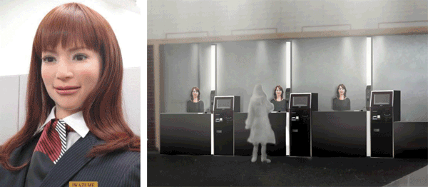
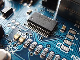

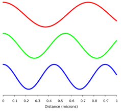
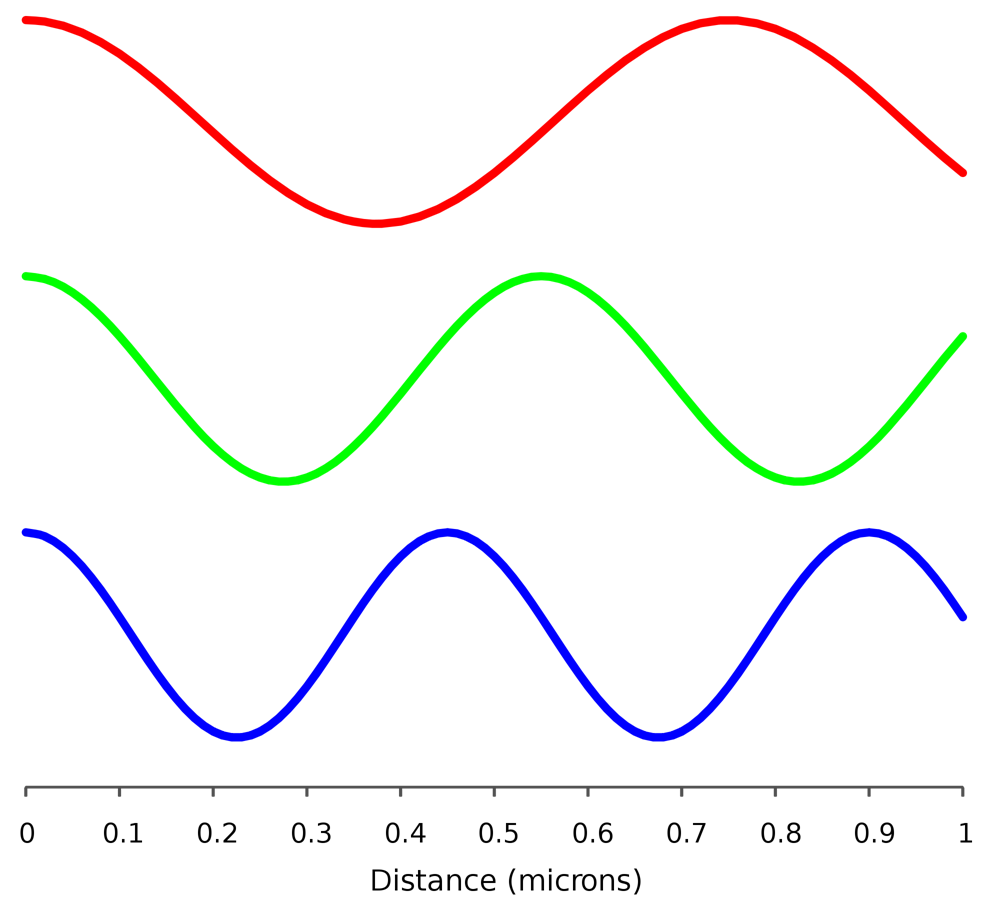

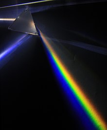


.svg)
.svg)
.svg)


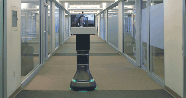
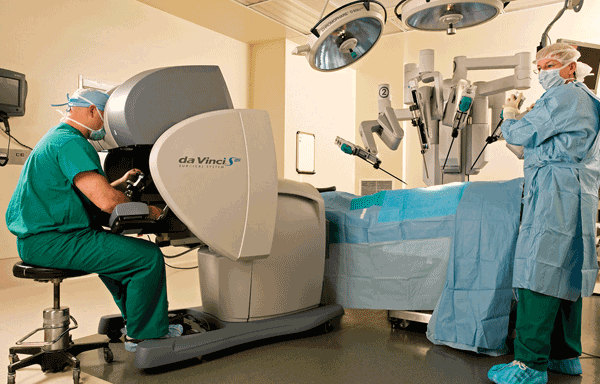
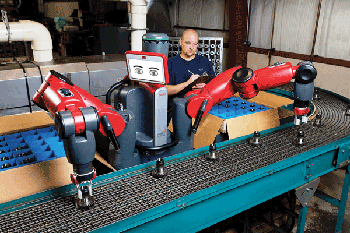


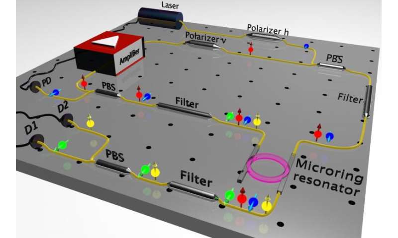


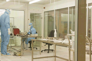

Tidak ada komentar:
Posting Komentar