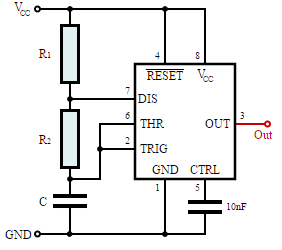
555 Tester circuit
Description.
NE555 is an IC which is widely used in timers and control circuits. A circuit for independent testing this IC is given here.
Here the NE555 is wired as an astable multivibrator. When the push button switch S1 is pressed the LEDs D1 & D2 will flash alternatively. That is when output is high D2 will glow & when output is low D3 will glow. The rate of flashing will depend on components R1,R2 & C1.
When push button S1 is pressed,C1 will start charging through R1&R2.When the voltage across C1 rises above 2 of 3 is the supply voltage the internal Flip Flop toggles . The pin 7 becomes low & C1 starts discharging. When the voltage across C1 goes below 1of 3 of supply voltage the internal Flip Flop resets & pin7 goes high. The C1 again starts charging.All this will take place if the IC is healthy.
According to the frequency of this charging & discharging D1&D2 will flash. From these observations we can conclude that IC NE555 is faulty or not .
Circuit diagram with Parts list.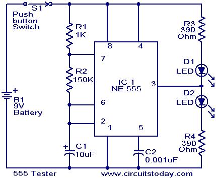
Notes.
- Assemble the circuit on a good quality PCB or common board.
- Power the circuit from a 9V radio battery.
- If D1 and D2 flashes on the pressing of S1,we can assume that the IC is working
Q . I Understanding 555 Timer IC

555 Timer IC is one of the commonly used IC among students and hobbyists. There are a lot of applications of this IC, mostly used as vibrators like, ASTABLE MULTIVIBRATOR, MONOSTABLE MULTIVIBRATOR, and BISTABLE MULTIVIBRATOR. You can find here some circuits based on 5555 IC. This tutorial covers different aspects of 555 Timer IC and explains its working in details. So lets first understand what are astable, monostable and bistable vibrators.
ASTABLE MULTIVIBRATOR
This means there will be no stable level at the output. So the output will be swinging between high and low. This character of unstable output is used as clock or square wave output for many applications.
MONOSTABLE MULTIVIBRATOR
This means there will be one stable state and one unstable state. The stable state can be chosen either high or low by the user. If the stable output is selected high, then the timer always tries to put high at output. So when a interrupt is given, the timer goes low for a short time and since the low state is unstable it goes to high after that time. If the stable state is chosen low, with interrupt the output goes high for a short time before coming to low.
This means both the output states are stable. With each interruption the output changes and stays there. For instance the output is considered high now with interruption it goes low and it stays low. By the next interruption it goes high.
Important Characterstics of 555 Timer IC
NE555 IC is a 8 pin device. The important electrical characteristics of timer are that it should not be operated above 15V, it means the source voltage cannot be higher than 15v. Second, we cannot draw more than 100mA from the chip. If don't follow these, IC would be burnt and damaged.
Working Explanation
The timer basically consists of two primary building blocks and they are:
1.Comparators (two) or two op-amp
2.One SR flip-flop (set reset flip-flop)
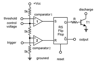
As shown in the above figure there are only two important components in timer, they are comparator and flip-flop. Lets understand what are comparators and flip flops.
Comparators: comparator is simply a device that compares the voltages at the input terminals (inverting (- VE) and non-inverting (+VE) terminals). So depending on the difference in the positive terminal and negative terminal at input port, the output of the comparator is determined.
For example consider positive input terminal voltage be +5V and negative input terminal voltage be +3V. The difference is, 5-3=+2v. Since the difference is positive we get the positive peak voltage at the output of the comparator.
For another example, if positive terminal voltage is +3V and negative input terminal voltage be +5V. The difference is +3-+5=-2V, since the difference input voltage is negative. The output of comparator will be negative peak voltage.
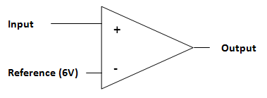
If for an example consider the positive input terminal as INPUT and the negative input terminal as REFERENCE as shown in above figure. So the difference of voltage between INPUT and REFERNCE is positive we get a positive output from the comparator. If the difference is negative then we will get negative or ground at the comparator output.
Flip-Flop: The flip-flop is a memory cell, it can store one bit of data. In the figure we can see the truth table of SR flip-flop.
There are four states to a flip-flop for two inputs; however we need to understand only two states of the flip- flop for this case.
| S | R | Q | Q' (Q bar) |
| 0 | 1 | 0 | 1 |
| 1 | 0 | 1 | 0 |
Now as show in the table, for set and reset inputs we get the respective outputs. If there is a pulse at the set pin and a low level at reset, then flip-flop stores the value one and puts high logic at Q terminal. This state continues until the reset pin gets a pulse while set pin has low logic. This resets the flip-flop so the output Q goes low and this state continues until the flip-flop is set again.
By this way the flip-flop stores one bit of data. Here another thing is Q and Q bar are always opposite.
In a timer the comparator and flip-flop are brought together.
Consider 9V is supplied to the timer, because of the voltage divider formed by the resistor network inside the timer as shown in the block diagram; there will be voltage at the comparator pins. So because of the voltage divider network we will have +6V at the negative terminal of the comparator one. And +3V at the positive terminal of the second comparator.
One another thing is comparator one output is connected to reset pin of flip-flop, so it the comparator one output goes high from low then the flip-flop will reset. And on the other hand the second comparator output is connected to set pin of flip-flop, so if the second comparator output goes high from low the flip-flop sets and stores ONE.
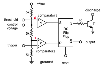
Now if we observe carefully, for a voltage less than +3V at the trigger pin (negative input of second comparator), the output of the comparator goes low from high as discussed earlier. This pulse sets the flip-flop and it stores a value one.
Now if we apply a voltage higher than +6V at the threshold pin (positive input of comparator one) , the output of comparator goes from low to high. This pulse resets the flip-flop and the flip-flip store zero.
Another thing happens during reset of flip-flop, when it resets the discharge pin gets connected to ground as Q1 gets turned on. Q1 transistor turns on because the Qbar is high at reset and is connected to Q1 base.
In astable configuration the capacitor connected here discharges during this time and so the output of timer will be low during this time.In astable configuration the time during the capacitor charges the trigger pin voltage will be less than +3V and so the flip-flop will store one and the output will be high.
In an astable configuration as shown in figure,
The output signal frequency depends on RA, RB resistors and capacitor C. The equation is given as,
Frequency(F) = 1/(Time period) = 1.44/((RA+RB*2)*C).
Here RA, RB are resistance values and C is capacitance value. By putting the resistance and capacitance values in above equation we get the frequency of output square wave.
High Level logic time is given as, TH= 0.693*(RA+RB)*C
Low Level logic time is given as, TL= 0.693*RB*C
Duty ratio of the output square wave is given as, Duty Cycle= (RA+RB)/(RA+2*RB).
555 Timer Pin Diagram and Descriptions
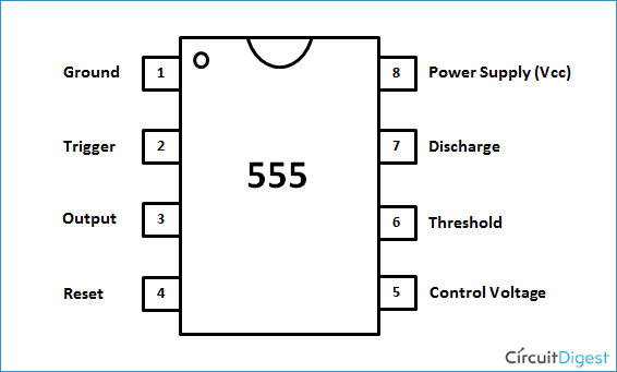
Now as shown in figure, there are eight pins for a 555 Timer IC namely,
1.Ground.
2.Trigger.
3.Output.
4.Reset.
5.Control
6.Threshold.
7.Discharge
8.Power or Vcc
Pin 1. Ground: This pin has no special function what so ever. It is connected to ground as usual. For the timer to function, this pin must and should be connected to ground.
Pin 8. Power or VCC: This pin also has no special function. It is connected to positive voltage. For the timer to function to work, this pin must be connected to positive voltage of range +3.6v to +15v.
Pin 4. Reset: As discussed earlier, there is a flip-flop in the timer chip. The output of flip-flop controls the chip output at pin3 directly.
Reset pin is directly connected to MR (Master Reset) of the flip-flop. On observation we can observe a small circle at the MR of flip-flop. This bubble represents the MR (Master Reset) pin is active LOW trigger. That means for the flip-flop to reset the MR pin voltage must go from HIGH to LOW. With this step down logic the flip-flop gets hardly pulled down to LOW. So the output goes LOW, irrespective of any pins.
This pin is connected to VCC for the flip-flop to stop from hard resetting.
Pin 3. OUTPUT: This pin also has no special function. This pin is drawn from PUSH-PULL configuration formed by transistors.
The push pull configuration is shown in figure. The bases of two transistors are connected to flip-flop output. So when logic high appears at the output of flip-flop, the NPN transistor turns on and +V1 appears at the output. When logic appeared at the output of flip-flop is LOW, the PNP transistor gets turned on and the output pulled down to ground or –V1 appears at the output.
Thus how the push-pull configuration is used to get square wave at the output by control logic from flip-flop. The main purpose of this configuration is to get the load off flip-flop back. Well the flip-flop obviously cannot deliver 100mA at the output.
Well until now we discussed pins that do not alter the condition of output at any condition. The remaining four pins are special because they determine the output state of timer chip, we will discuss each of them now.
Pin 5. Conrol Pin: The control pin is connected from the negative input pin of comparator one.
Consider for a case the voltage between VCC and GROUND is 9v. Because of the voltage divider in the chip as observed in figure3 of page8, The voltage at the control pin will be VCC*2/3 (for VCC = 9, pin voltage=9*2/3=6V ).
The function of this pin to give the user the directly control over first comparator. As shown in above figure the output of comparator one is fed to the reset of flip-flop. At this pin we can put a different voltage, say if we connect it to +8v. Now what happens is, the THRESHOLD pin voltage must reach +8V to reset the flip-flop and to drag the output down.
For normal case, the V-out will go low once the capacitor gets charge up to 2/3VCC (+6V for 9V supply). Now since we put up a different voltage at control pin (comparator one negative or reset comparator).
Capacitor should charge until its voltage reaches the control pin voltage. Because of this force capacitor charging, the turn on time and turn off time of signal changes. So the output experiences a different turn on torn off ration.
Normally this pin is pulled down with a capacitor. To avoid unwanted noise interference with the working.
Pin 2. TRIGGER: Trigger pin is dragged from the negative input of comparator two. The comparator two output is connected to SET pin of flip-flop. With the comparator two output high we get high voltage at the timer output. So we can say the trigger pin controls timer output.
Now here what to observe is, low voltage at the trigger pin forces the output voltage high, since it is at inverting input of second comparator. The voltage at the trigger pin must go below VCC*1/3 (with VCC 9v as assumed, VCC*(1/3)=9*(1/3)=3V). So the voltage at the trigger pin must go below 3V (for a 9v supply) for the output of timer to go high.
If this pin is connected to ground, the output will be always high.
Pin 6. THRESHOLD: Threshold pin voltage determines when to reset the flip-flop in the timer. The threshold pin is drawn from positive input of comparator1.
Here the voltage difference between THRESOLD pin and CONTROL pin determines the comparator 2 output and so the reset logic. If the voltage difference is positive the flip-flop gets resetted and output goes low. If the difference in negative, the logic at SET pin determines the output.
If the control pin is open. Then a voltage equal to or greater than VCC*(2/3) (i.e.6V for a 9V supply) will reset the flip-flop. So the output goes low.
So we can conclude that THRESHOLD pin voltage determines when the output should go low, when the control pin is open.
Pin 7. DISCHARGE: This pin is drawn from the open collector of transistor. Since the transistor (on which discharge pin got taken, Q1) got its base connected to Qbar. Whenever the ouput goes low or the flip-flop gets resetted, the discharge pin is pulled to ground. Because Qbar will be high when Q is low, So the transistor Q1 gets turns ON as base of transistor got power.
This pin usually discharges capacitor in ASTABLE configuration, so the name DISCHARGE.
 Simple Flashing LED using 555 Timer IC
While getting started with electronics, you would like to make some simple circuits to get acquainted with basic circuit designing concepts. Here is one for you – An LED Flasher Circuit Diagram. Using some common easily available electronic components and an easy to understand schematic, this tutorial will show you how to make an LED glow and fade on a certain interval. So here is the step by step guide to make this flashing LED circuit.
Circuit Components
- 555 Timer IC
- 1uF Capacitor
- 470k Ohm Resistor
- 1k Ohm Resistors (2)
- 9v Battery
Circuit Diagram

555 timer IC is used here in astable operating mode which generates a continuous output in the form of square wave via pin 3 which turns the LED on and off. You can read here more about the different operating modes and basic concepts of 555 timer IC.
How to Make the LED Flasher Circuit: Step By Step
- Collect all the required components and get ready! Place the 555 timer IC on breadboard as per shown in the breadboard setup image given above.
- Connect pin 1 of 555 timer IC to the ground. You can see the pin structure of 555 timer IC in the pin diagram shown below.
- Connect pin 2 to the positive end of capacitor. The longer lead of a polarized capacitor is the positive and the shorter one is negative. Connect the negative lead of the capacitor with the ground of battery.
- Also connect the pin 2 with pin 6 of the 555 timer IC.
- Connect the pin 3 which is the output pin with the positive lead of LED using 1kΩ resistor. Negative lead of LED needs to be connected with the ground.
- Connect pin 4 with the positive end of battery.
- Pin 5 doesn’t connect with anything.
- Connect pin 6 with pin 7 using a 470kΩ resistor.
- Connect pin 7 with the positive end of battery using 1kΩ resistor.
- Connect pin 8 with the positive end of battery.
- Finally connect the battery leads with the breadboard to start the power supply in the circuit.
Once you connect battery in the circuit, it should flash the LED. If it doesn’t work, check the connections again. Also make sure that battery is connected properly in the breadboard and power is reaching to the components of circuit. Here you can change the flashing speed of LED by changing the capacitor with different capacitance. If you want to add more LEDs in this flashing LED circuit, connect them parallel with the first LED using proper resistors.
Q . III 12V to 220V DC to AC Converter Circuit

This DIY 12V to 220V DC to AC converter is built with CMOS 4047 that is the main component of this small voltage converter that transforms a 12VDC into 220VAC. 4047 is used as an astable mutivibrator, at pins 10 and 11 will have a symmetrical rectangular signal (square wave) which is amplified by 2 Darlington transistors and finally reach the secondary coil of mains transformer (2x10V/60W).
60 Watt DC to AC Converter Circuit Schematic
I used BD651 transistors instead of BD699.
The CD4047B is capable of operating in either the monostable or astable mode. It requires an external capacitor (between pins 1 and 3) and an external resistor (between pins 2 and 3) to determine the output pulse width in the monostable mode, and the output frequency in the astable mode.
4047 IC Applications
- Frequency discriminators
- Timing circuits
- Time-delay applications
- Envelope detection
- Frequency multiplication
- Frequency division
Q . III CD4047 Astable/Monostable Multivibrator
Today we are going to examine an older but still highly useful integrated circuit – the 4047 Astable/Monostable multivibrator:

My reason for doing this is to demonstrate another way to create a square-wave output for digital circuits (astable mode) and also generate single pulses (monostable mode). Sometimes one can get carried away with using a microcontroller by default – and forget that there often can be simpler and much cheaper ways of doing things. And finally, the two can often work together to solve a problem.
What is a multivibrator? In electronics terms this means more than one vibrator. It creates an electrical signal that changes state on a regular basis (astable) or on demand (monostable). You may recall creating monostable and astable timers using the 555 timer described in an earlier article. One of the benefits of the 4047 is being able to do so as well, but with fewer external components. Here is the pinout diagram for a 4047 (from the Fairchild data sheet):

Note that there are three outputs, Q,
That was an example of the astable mode. The circuit used is shown below. The only drawback of using a 4047 is that you cannot alter the duty cycle of your astable output – it will always be 50% high and 50% low. The oscillator output is not guaranteed to have a 50% duty cycle, but comes close. The time period (and therefore the frequency) is determined by two components – R1 and the capacitor:
[Quick update – in the schematic below, also connect 4047 pin 14 to +5V]

 And as the frequency from the OSC out pin is twice that of Q or
However the most useful formula would allow you to work with the values of R and C to use for a desired frequency f:

When calculating your values, remember that you need to work with whole units, such as Farads and Ohms- not microfarads, mega-ohms, etc. This chart of SI prefixes may be useful for conversions.
The only thing to take note of is the tolerance of your resistor and capacitor. If you require a certain, exact frequency try to use some low-tolerance capacitors, or replace the resistor with a trimpot of a value just over your required resistor value. Then you can make adjustments and measure the result with a frequency counter. For example, when using a value of 0.1uF for C and 15 k ohm for R, the theoretical frequency is 151.51 Hz; however in practice this resulted with a frequency of 144.78 Hz. Don’t forget that the duty cycle is not guaranteed to be 50% from the OSC out pin .
Now for some more more explanation about the 4047. You can activate the oscillations in two ways, via a high signal into pin 5 (pin 4 must then be low) or via a low signal into pin 4 (and pin 5 must be low). Setting pin 9 high will reset the oscillator, so Q is low and Q is high.
The monostable mode is also simple to create and activate. I have not made a video clip of monstable operation, as this would only comprise of staring at an LED. However, here is an example circuit with two buttons added, one to trigger the pulse (or start it), and another to reset the timer (cancel any pulse and start again):
[Quick update – in the schematic below, also connect 4047 pin 14 to +5V]
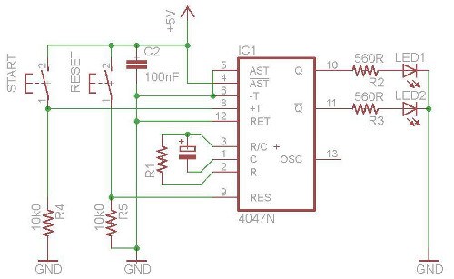
The following formula is used to calculate the duration of the pulse time:
 Where time is in seconds, R is Ohms, and C is Farads. Once again, the OSC output pin also has a modified output – it’s time period will be 1.2RC.
To conclude, the 4047 offers a simple and cheap way to generate a 50% duty cycle square wave or use as a monostable timer. The cost is low and the part is easy to source.

Q . III How to Understand IC 4017 Pinouts – Explained in Simple Words
Introduction
Technically it is called the Johnsons 10 stage decade counter divider. The name suggest two things, it’s something to do with number 10 and counting/dividing.
The number 10 is connected with the number of outputs this IC has, and these outputs become high in sequence in response to every high clock pulse applied at its input clock pin out.
It means, all its 10 outputs will go through one cycle of high output sequencing from start to finish in response to 10 clocks received at its input. So in a way it is counting and also dividing the input clock by 10 and hence the name.

The pinout which are marked as outputs are the pins which become logic high one after the other in a sequence in response to clock signals at pin#14 of the IC.
Therefore with the first clock pulse at pin#14 the first output pinout in the order which is the pin#3 goes high first, then it shuts off and simultaneously the next pin #2 becomes high, then this pin goes low and simultaneously the preceding pin #4 becomes high...... and so on until the last pin #11 becomes high.
To be precise, the sequencing movement happens through the pinouts: 3, 2, 4, 7, 10, 1, 5, 6, 9, 11...
After pin#11 the IC internally resets and reverts the logic high at pin #3 to repeat the cycle.
This sequencing and resetting is successfully carried out only as long as pin#15 is grounded or held at a logic low, otherwise the IC can malfunction. If it is held high, then the sequencing will not happen and the logic at pin#3 will stay locked.
You can see that the logic shift happens in response only to the positive clock or positive edge at pin#14 of the IC 4017. The sequence does not respond to the negative pulses or clocks
The number 10 is connected with the number of outputs this IC has, and these outputs become high in sequence in response to every high clock pulse applied at its input clock pin out.
It means, all its 10 outputs will go through one cycle of high output sequencing from start to finish in response to 10 clocks received at its input. So in a way it is counting and also dividing the input clock by 10 and hence the name.

Understanding pinout Function of IC 4017
Let’s understand the pin outs of the IC 4017 in details and from a newcomer’s point of view: Looking at the figure we see that the device is a 16 pin DIL IC, the pin out numbers are indicated in the diagram with their corresponding assignment names.The pinout which are marked as outputs are the pins which become logic high one after the other in a sequence in response to clock signals at pin#14 of the IC.
Therefore with the first clock pulse at pin#14 the first output pinout in the order which is the pin#3 goes high first, then it shuts off and simultaneously the next pin #2 becomes high, then this pin goes low and simultaneously the preceding pin #4 becomes high...... and so on until the last pin #11 becomes high.
To be precise, the sequencing movement happens through the pinouts: 3, 2, 4, 7, 10, 1, 5, 6, 9, 11...
After pin#11 the IC internally resets and reverts the logic high at pin #3 to repeat the cycle.
Please note that the word “high” means a positive voltage that may be equal to the supply voltage of the IC, so when I say the outputs become high in a sequential manner means the outputs produce a positive voltage which shifts in a sequential manner from one output pin to the next, in a “running” DOT manner.
Now the above explained sequencing or shifting of the output logic from one one output pin to the next is able to run only when a clock signal is applied to the clock input of the IC which is pin #14.
Remember, if no clock is applied to this input pin#14, it must be assigned either to a positive supply or a negative supply, but should never be kept hanging or unconnected, as per the standard rules for all CMOS inputs.
The clock input pin #14 only responds to positive clocks or a positive signal and with each consequent positive peak signal, the output of the IC shifts or becomes high in sequence, the sequencing of the outputs are in the order of pinouts #3, 2, 4, 7, 10, 1, 5, 6, 9, 11.
Pin #13 may be considered as the opposite of pin #14 and this pin out will respond to negative peak signals, if a clock is applied to this pin, producing the same results with the outputs as discussed above.
However normally this pin out is never used for applying the clock signals, instead pin #14 is taken as the standard clock input.
However, pin #13 needs to be assigned a ground potential, that means, must be connected to the ground for enabling the IC to function.
In case pin #13 is connected to positive, the whole IC will stall and the outputs will stop sequencing and stop responding to any clock signal applied at pin #14.
Pin #15 of the IC is the reset pin input. The function of this pin is to revert the sequence back to the initial state in response to a positive potential or supply voltage, meaning the sequencing comes back to pin #3 and begins the cycle afresh, if a momentary positive supply is applied to pin #15.
If the positive supply is held connected to this pin #15, again stalls the output from sequencing and the output clamps to pin #3 making this pinout high and fixed.
Therefore to make the IC function, pin #15 should always be connected to ground.
If this pinout is intended to be used as a reset input, then it may be clamped to ground with a series resistor of 100K or any other high value, so that a positive supply now can be freely introduced to it, whenever the IC is required to be reset.
Pin #8 is the ground pin and must be connected to the negative of the supply, while pin #16 is the positive and should be terminated to the positive of the voltage supply.
Pin #12 is the carry out, and is irrelevant unless many ICs are connected in series, we will discuss it some other day. Pin #12 can be left open.
Have specific questions?? please feel free to ask them through your comments...all will be thoroughly addressed by me.
Application LED Chaser Circuit using IC 4017 and IC555
The following example GIF circuit shows how the pinouts of a IC 4017 is usually wired with an oscillator for obtaining the sequential logic high outputs. Here the outputs are connected to LEDs for indicating the sequential shift of the logics in response to each clock pulse generated by the IC 555 oscillator at pin#14 of the IC 4017.You can see that the logic shift happens in response only to the positive clock or positive edge at pin#14 of the IC 4017. The sequence does not respond to the negative pulses or clocks

======== MA THE MATIC FIGURE EL 4047 LGIGO IC 555 DO VIBRATE =======
Tidak ada komentar:
Posting Komentar